SLUSAF8E July 2011 – January 2016 TPS40322
PRODUCTION DATA.
- 1 Features
- 2 Applications
- 3 Description
- 4 Revision History
- 5 Pin Configuration and Functions
- 6 Specifications
-
7 Detailed Description
- 7.1 Overview
- 7.2 Functional Block Diagram
- 7.3
Feature Description
- 7.3.1 Voltage Reference
- 7.3.2 Output Voltage Setting
- 7.3.3 Input Voltage Feedforward
- 7.3.4 Current Sensing
- 7.3.5 Overcurrent Protection
- 7.3.6 Two-Phase Mode, Remote Sense Amplifier, and Current Sharing Loop
- 7.3.7 Start-Up and Shutdown
- 7.3.8 Switching Frequency and Master or Slave Synchronization
- 7.3.9 Overvoltage and Undervoltage Fault Protection
- 7.3.10 Input Undervoltage Lockout (UVLO)
- 7.3.11 Power Good
- 7.3.12 Thermal Shutdown
- 7.3.13 Connection of Unused Pins
- 7.4 Device Functional Modes
-
8 Applications and Implementation
- 8.1 Application Information
- 8.2
Typical Applications
- 8.2.1
Dual-Output Configuration from 12-V Nominal to 1.2-V and 1.8-V DC-to-DC Converter Using the TPS40322
- 8.2.1.1 Design Requirements
- 8.2.1.2
Detailed Design Procedure
- 8.2.1.2.1 Selecting a Switching Frequency
- 8.2.1.2.2 Inductor Selection (L1)
- 8.2.1.2.3 Output Capacitor Selection (C10 through C16)
- 8.2.1.2.4 Peak Current Rating of Inductor
- 8.2.1.2.5 Input Capacitor Selection (C3 through C6)
- 8.2.1.2.6 MOSFET Selection (Q1)
- 8.2.1.2.7 ILIM Resistor (R2)
- 8.2.1.2.8 Feedback Divider (R10, R14)
- 8.2.1.2.9 Compensation: (R11, R12, C17, C19, C21)
- 8.2.1.2.10 Boot-Strap Capacitor (C7)
- 8.2.1.2.11
General Device Components
- 8.2.1.2.11.1 Synchronization (SYNC Pin)
- 8.2.1.2.11.2 RT Resistor (R6)
- 8.2.1.2.11.3 Differential Amplifier Out (DIFFO Pin)
- 8.2.1.2.11.4 EN/SS Timing Capacitors (C8)
- 8.2.1.2.11.5 Power Good (PG1, PG2 Pins)
- 8.2.1.2.11.6 Phase Set (PHSET Pin)
- 8.2.1.2.11.7 UVLO Programming Resistors (R1 and R3)
- 8.2.1.2.11.8 VDD Bypass Capacitor (C2)
- 8.2.1.2.11.9 VBP6 Bypass Capacitor (C18)
- 8.2.1.3 Application Curves
- 8.2.2 Two-Phase, Single Output Configuration from 12-V nominal to 1.2-V DC-to-DC Converter Using the TPS40322
- 8.2.1
Dual-Output Configuration from 12-V Nominal to 1.2-V and 1.8-V DC-to-DC Converter Using the TPS40322
- 9 Power Supply Recommendations
- 10Layout
- 11Device and Documentation Support
- 12Mechanical, Packaging, and Orderable Information
パッケージ・オプション
メカニカル・データ(パッケージ|ピン)
- RHB|32
サーマルパッド・メカニカル・データ
- RHB|32
発注情報
1 Features
- Dual-Output or Two-Phase Synchronous Buck Controller
- 180° Out-of-Phase Reduces Input Ripple
- Input Voltage Range: 3 V to 20 V
- Output Voltage Range: 0.6 V to 5.6 V
- Adjustable Frequency: 100 kHz to 1 MHz
- Bidirectional SYNC Pin With 0°/180° or 90°/270° Phase Shift
- Voltage Mode Control With Input Feedforward
- Accurate Current Sharing for Two-Phase Operation
- Individual Power Good Outputs
- Individual Enable and Programmable Soft Start, With Pre-Bias Start-Up
- ±0.5%, 600-mV Reference
- Output UV/OV Protection and Input Undervoltage Lockout
- Individual Overcurrent Limit Setting
- Hiccup Overcurrent Protection
- Accurate Inductor DCR or Resistive Current Sensing
- Remote Sense for Two-Phase Applications
- Internal N-Channel FET Drivers
- Integrated Bootstrap Switches
- Available in 5-mm × 5-mm 32-Pin VQFN Package
2 Applications
- Multiple Rail Systems
- Telecom Base Station
- Switcher and Router Networking
- xDSL Broadband Access
- Server and Storage System
3 Description
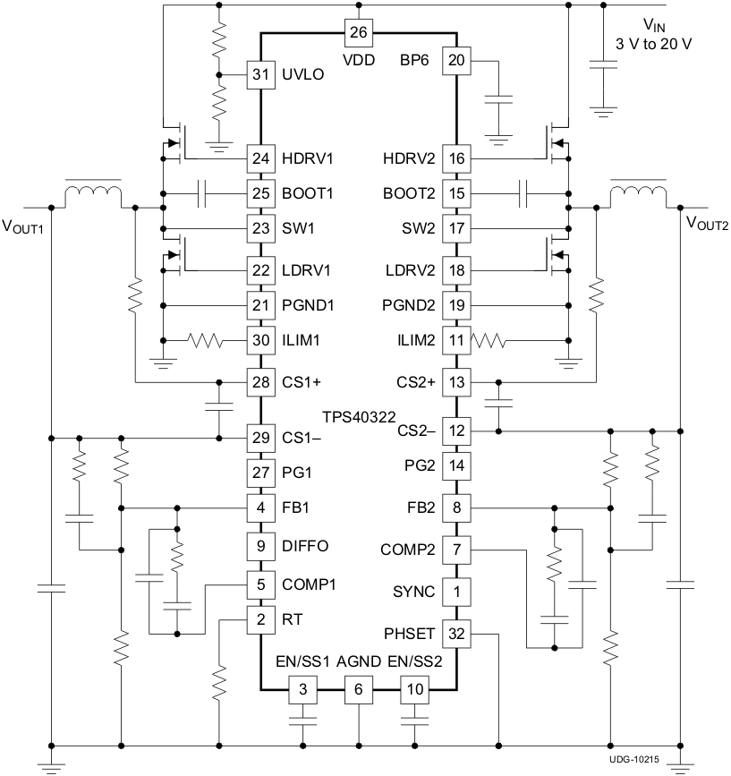
The TPS40322 device is a dual-output, synchronous buck controller. It can also be configured as a single-output, two-phase controller. The 180° out-of-phase operation reduces the input current ripple and extends the input capacitor lifetime. Bidirectional master and slave synchronization function provides evenly distributed phase shift for a four-output system that reduces input ripple further and attenuates the system noise.
The wide input range can support 3.3-V, 5-V, and
12-V buses. The accurate reference voltage satisfies the precision voltage needed by ASICs and potentially reduces the output capacitance requirement. Separate PGOOD signals provide flexibility for system monitoring and sequencing. The two channels are independently controlled and each soft-start time is programmable. Voltage mode control is implemented to reduce noise sensitivity and also ensures low duty ratio conversion.
Device Information(1)
| PART NUMBER | PACKAGE | BODY SIZE (NOM) |
|---|---|---|
| TPS40322 | VQFN (32) | 5.00 mm × 5.00 mm |
- For all available packages, see the orderable addendum at the end of the data sheet.
4 Revision History
Changes from D Revision (December 2013) to E Revision
- Added ESD Ratings table, Feature Description section, Device Functional Modes, Application and Implementation section, Power Supply Recommendations section, Layout section, Device and Documentation Support section, and Mechanical, Packaging, and Orderable Information section Go
- Updated the thermal data to new values Go
Changes from C Revision (JANUARY 2013) to D Revision
- Added information regarding the appropriate output voltage range when using the remote sense amplifier in the Two-Phase Mode, Remote Sense Amplifier, and Current Sharing Loop sectionGo
Changes from B Revision (JUNE 2012) to C Revision
- Added clarity to ABSOLUTE MAXIMUM RATINGS tableGo
Changes from A Revision (JANUARY 2012) to B Revision
- Changed all references of "multi-phase" to "two-phase" throughout documentGo
- Added clarity to SIMPLIFIED APPLICATION CIRCUIT.Go
- Added "When not being used, SYNC must be left floating" to SYNC description in PIN FUNCTIONS table.Go
- Added clarity to Functional Block DiagramGo
- Added clarity to Figure 15Go
- Added clarity to Figure 16Go
- Added clarity to Figure 17Go
- Added clarity to Figure 18Go
- Added clarity to Figure 19Go
- Changed "This design limits the maximum voltage drop across the current sense inputs, VCS(max), to 60 mV." to "This design limits the maximum voltage drop across the current sense inputs, VCS(max), to 50 mV." in ILIM Resistor (R2) section.Go
- Changed Equation 23Go
- Changed Output current = 10 (max) to Output current = 30 (max) in Table 7 Go
Changes from * Revision (JUNE 2011) to A Revision
