SLUSAS9B NOVEMBER 2013 – December 2014 TPS53915
PRODUCTION DATA.
- 1 Features
- 2 Applications
- 3 Description
- 4 Revision History
- 5 Pin Configuration and Functions
- 6 Specifications
-
7 Detailed Description
- 7.1 Overview
- 7.2 Functional Block Diagrams
- 7.3
Feature Description
- 7.3.1 Powergood
- 7.3.2 D-CAP3 Control and Mode Selection
- 7.3.3 D-CAP3 Mode
- 7.3.4 Sample and Hold Circuitry
- 7.3.5 Adaptive Zero-Crossing
- 7.3.6 Forced Continuous-Conduction Mode
- 7.3.7 Current Sense and Overcurrent Protection
- 7.3.8 Overvoltage and Undervoltage Protection
- 7.3.9 Out-Of-Bounds Operation (OOB)
- 7.3.10 UVLO Protection
- 7.3.11 Thermal Shutdown
- 7.4 Device Functional Modes
- 7.5
Programming
- 7.5.1 The PMBus General Descriptions
- 7.5.2 PMBus Slave Address Selection
- 7.5.3 PMBus Address Selection
- 7.5.4 Supported Formats
- 7.5.5 Supported PMBus Commands
- 7.5.6 CLEAR_FAULTS [03h] (Send Byte)
- 7.5.7 STORE_DEFAULT_ALL [11h] (Send Byte)
- 7.5.8 RESTORE_DEFAULT_ALL [12h] (Send Byte)
- 7.5.9 STATUS_WORD [79h] (Read Word)
- 7.5.10 CUSTOM_REG (MFR_SPECIFIC_00) [D0h] (R/W Byte)
- 7.5.11 DELAY_CONTROL (MFR_SPECIFIC_01) [D1h] (R/W Byte)
- 7.5.12 MODE_SOFT_START_CONFIG (MFR_SPECIFIC_02) [D2h] (R/W Byte)
- 7.5.13 FREQUENCY_CONFIG (MFR_SPECIFIC_03) [D3h] (R/W Byte)
- 7.5.14 VOUT_ADJUSTMENT (MFR_SPECIFIC_04) [D4h] (R/W Byte)
- 7.5.15 Output Voltage Fine Adjustment Soft Slew Rate
- 7.5.16 VOUT_MARGIN (MFR_SPECIFIC_05) [D5h] (R/W Byte)
- 7.5.17 Output Voltage Margin Adjustment Soft-Slew Rate
- 7.5.18 UVLO_THRESHOLD (MFR_SPECIFIC_06) [D6h]
- 8 Application and Implementation
- 9 Power Supply Recommendations
- 10Layout
- 11Device and Documentation Support
- 12Mechanical, Packaging, and Orderable Information
パッケージ・オプション
メカニカル・データ(パッケージ|ピン)
- RVE|28
サーマルパッド・メカニカル・データ
- RVE|28
発注情報
7 Detailed Description
7.1 Overview
The TPS53915 is a high-efficiency, single-channel, synchronous-buck converter. The device suits low-output voltage point-of-load applications with 12-A or lower output current in computing and similar digital consumer applications. The TPS53915 features proprietary D-CAP3 mode control combined with adaptive on-time architecture. This combination builds modern low-duty-ratio and ultra-fast load-step-response DC-DC converters in an ideal fashion. The output voltage ranges from 0.6 V to 5.5 V. The conversion input voltage ranges from 1.5 V to 18 V and the VDD input voltage ranges from 4.5 V to 25 V. The D-CAP3 mode uses emulated current information to control the modulation. An advantage of this control scheme is that it does not require a phase-compensation network outside which makes the device easy-to-use and also allows low-external component count. Adaptive on-time control tracks the preset switching frequency over a wide range of input and output voltage while increasing switching frequency as needed during load-step transient.
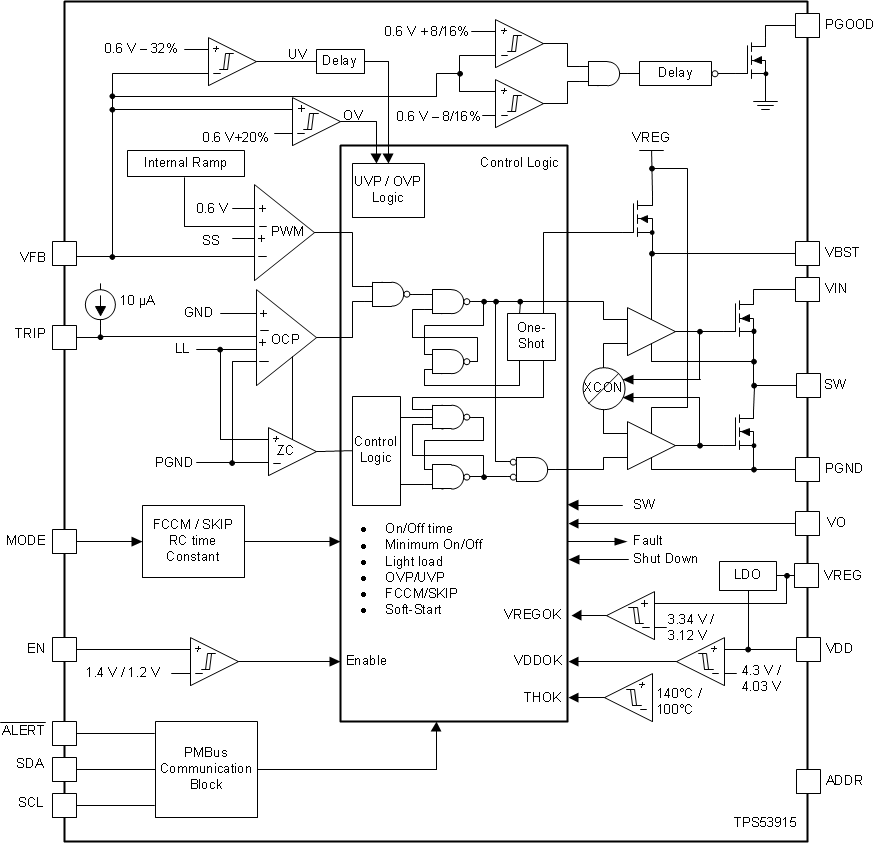
7.2 Functional Block Diagrams
7.3 Feature Description
7.3.1 Powergood
The TPS53915 has powergood output that indicates high when switcher output is within the target. The power-good function is activated after the soft-start operation is complete. If the output voltage becomes within ±8% of the target value, internal comparators detect the power-good state and the power-good signal becomes high after a 1-ms internal delay. If the output voltage goes outside of ±16% of the target value, the power-good signal becomes low after a 2-μs internal delay. The power-good output is an open-drain output and must be pulled-up externally.
7.3.2 D-CAP3 Control and Mode Selection
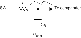 Figure 39. Internal RAMP Generation Circuit
The TPS53915 uses D-CAP3 mode control to achieve fast load transient while maintaining the ease-of-use feature. An internal RAMP is generated and fed to the VFB pin to reduce jitter and maintain stability. The amplitude of the ramp is determined by the R-C time-constant as shown in Figure 39. At different switching frequencies, (fSW) the R-C time-constant varies to maintain relatively constant RAMP amplitude.
The default switching frequency (fSW) is pre-set at 400 kHz. The switching frequency can be changed via PMBus function (see Table 13).
7.3.3 D-CAP3 Mode
From small-signal loop analysis, a buck converter using the D-CAP3 mode control architecture can be simplified as shown in Figure 40.
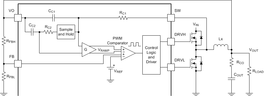 Figure 40. D-CAP3 Mode
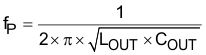
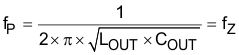
The D-CAP3 control architecture includes an internal ripple generation network enabling the use of very low-ESR output capacitors such as multi-layered ceramic capacitors (MLCC). No external current sensing network or voltage compensators are required with D-CAP3 control architecture. The role of the internal ripple generation network is to emulate the ripple component of the inductor current information and then combine it with the voltage feedback signal to regulate the loop operation. For any control topologies supporting no external compensation design, there is a minimum and/or maximum range of the output filter it can support. The output filter used with the TPS53513 is a lowpass L-C circuit. This L-C filter has double pole that is described in Equation 1.
At low frequencies, the overall loop gain is set by the output set-point resistor divider network and the internal gain of the TPS53513. The low frequency L-C double pole has a 180 degree in phase. At the output filter frequency, the gain rolls off at a –40dB per decade rate and the phase drops rapidly. The internal ripple generation network introduces a high-frequency zero that reduces the gain roll off from –40dB to –20dB per decade and increases the phase to 90 degree one decade above the zero frequency.
The inductor and capacitor selected for the output filter must be such that the double pole of Equation 1 is located close enough to the high-frequency zero so that the phase boost provided by the high-frequency zero provides adequate phase margin for the stability requirement.
Table 1. Locating the Zero
| SWITCHING FREQUENCIES (fSW) (kHz) |
ZERO (fZ) LOCATION (kHz) |
|---|---|
| 250 and 300 | 6 |
| 400 and 500 | 7 |
| 600 and 750 | 9 |
| 850 and 1000 | 12 |
After identifying the application requirements, the output inductance should be designed so that the inductor peak-to-peak ripple current is approximately between 25% and 35% of the ICC(max) (peak current in the application). Use Table 1 to help locate the internal zero based on the selected switching frequency. In general, where reasonable (or smaller) output capacitance is desired, Equation 2 can be used to determine the necessary output capacitance for stable operation.
If MLCC is used, consider the derating characteristics to determine the final output capacitance for the design. For example, when using an MLCC with specifications of 10-µF, X5R and 6.3 V, the deratings by DC bias and AC bias are 80% and 50% respectively. The effective derating is the product of these two factors, which in this case is 40% and 4-µF. Consult with capacitor manufacturers for specific characteristics of the capacitors to be used in the system/applications.
Table 2 shows the recommended output filter range for an application design with the following specifications:
- Input voltage, VIN = 12 V
- Switching frequency, fSW = 600 kHz
- Output current, IOUT = 8 A
The minimum output capacitance is verified by the small signal measurement conducted on the EVM using the following two criteria:
- Loop crossover frequency is less than one-half the switching frequency (300 kHz)
- Phase margin at the loop crossover is greater than 50 degrees
For the maximum output capacitance recommendation, simplify the procedure to adopt an unrealistically high output capacitance for this type of converter design, then verify the small signal response on the EVM using the following one criteria:
- Phase margin at the loop crossover is greater than 50 degrees
As indicated by the phase margin, the actual maximum output capacitance (COUT(max)) can continue to go higher. However, small signal measurement (bode plot) should be done to confirm the design.
Select a MODE pin configuration as shown in Table 3 to double the R-C time constant option for the maximum output capacitance design and application. Select a MODE pin configuration to use single R-C time constant option for the normal (or smaller) output capacitance design and application.
The MODE pin also selects SKIP-mode or FCCM-mode operation.
Table 2. Recommended Component Values
| VOUT
(V) |
RLOWER
(kΩ) |
RUPPER
(kΩ) |
LOUT
(µH) |
COUT(min)
(µF) (1) |
CROSS- OVER (kHz) |
PHASE MARGIN (°) |
COUT(max)
(µF) (1) |
INTERNAL RC SETTING (µs) |
INDUCTOR ΔI/ICC(max) |
ICC(max)
(A) |
|---|---|---|---|---|---|---|---|---|---|---|
| 0.6 | 10 | 0 | 0.36 PIMB065T-R36MS |
3 × 100 | 247 | 70 | 40 | 33% | 8 | |
| 48 | 62 | 30 x 100 | 80 | |||||||
| 1.2 | 10 | 0.68 PIMB065T-R68MS |
9 × 22 | 207 | 53 | 40 | 33% | |||
| 25 | 84 | 30 x 100 | 80 | |||||||
| 2.5 | 31.6 | 1.2 PIMB065T-1R2MS |
4 × 22 | 185 | 57 | 40 | 34% | |||
| 11 | 63 | 30 x 100 | 80 | |||||||
| 3.3 | 45.3 | 1.5 PIMB065T-1R5MS |
3 × 22 | 185 | 57 | 40 | 33% | |||
| 9 | 59 | 30 x 100 | 80 | |||||||
| 5.5 | 82.5 | 2.2 PIMB065T-2R2MS |
2 × 22 | 185 | 51 | 40 | 28% | |||
| 7 | 58 | 30 x 100 | 80 |
For higher output voltage at or above 2.0 V, additional phase boost might be required in order to secure sufficient phase margin due to phase delay/loss for higher output voltage (large on-time (tON)) setting in a fixed on time topology based operation.
A feedforward capacitor placing in parallel with RUPPER is found to be very effective to boost the phase margin at loop crossover.
Table 3. Mode Selection and Internal RAMP RC Time Constant
| MODE SELECTION |
ACTION | RMODE
(kΩ) |
R-C TIME CONSTANT (µs) |
SWITCHING FREQUENCIES fSW (kHz) |
||
|---|---|---|---|---|---|---|
| Skip Mode | Pull down to GND | 0 | 60 | 275 | and | 325 |
| 50 | 425 | and | 525 | |||
| 40 | 625 | and | 750 | |||
| 30 | 850 | and | 1000 | |||
| 150 | 120 | 275 | and | 325 | ||
| 100 | 425 | and | 525 | |||
| 80 | 625 | and | 750 | |||
| 60 | 850 | and | 1000 | |||
| FCCM(1) | Connect to PGOOD | 20 | 60 | 275 | and | 325 |
| 50 | 425 | and | 525 | |||
| 40 | 625 | and | 750 | |||
| 30 | 850 | and | 1000 | |||
| 150 | 120 | 275 | and | 325 | ||
| 100 | 425 | and | 525 | |||
| 80 | 625 | and | 750 | |||
| 60 | 850 | and | 1000 | |||
| FCCM | Connect to VREG | 0 | 120 | 275 | and | 325 |
| 100 | 425 | and | 525 | |||
| 80 | 625 | and | 750 | |||
| 60 | 850 | and | 1000 | |||
7.3.4 Sample and Hold Circuitry
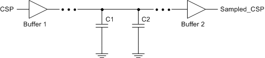 Figure 41. Sample and Hold Circuitry (Patent Pending)
The sample and hold circuitry is the difference between D-CAP3 and D-CAP2. The sample and hold circuitry, which is an advance control scheme to boost output voltage accuracy higher on the TPS53915, is one of features of the TPS53915. The sample and hold circuitry generates a new DC voltage of CSN instead of the voltage which is produced by RC2 and CC2 which allows for tight output-voltage accuracy and makes the TPS53915 more competitive.
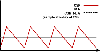 Figure 42. Continuous Conduction Mode (CCM) With Sample and Hold Circuitry
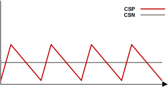 Figure 44. Continuous Conduction Mode (CCM) Without Sample and Hold Circuitry
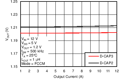 Figure 46. Output Voltage vs Output Current
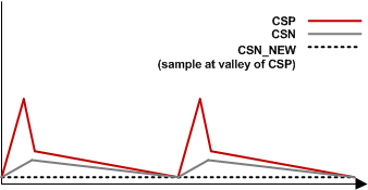 Figure 43. Discontinuous Conduction Mode (DCM) With Sample and Hold Circuitry
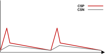 Figure 45. Discontinuous Conduction Mode (DCM) Without Sample and Hold Circuitry
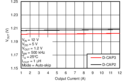 Figure 47. Output Voltage vs Output Current
7.3.5 Adaptive Zero-Crossing
The TPS53915 uses an adaptive zero-crossing circuit to perform optimization of the zero inductor-current detection during skip-mode operation. This function allows ideal low-side MOSFET turn-off timing. The function also compensates the inherent offset voltage of the Z-C comparator and delay time of the Z-C detection circuit. Adaptive zero-crossing prevents SW-node swing-up caused by too-late detection and minimizes diode conduction period caused by too-early detection. As a result, the device delivers better light-load efficiency.
7.3.6 Forced Continuous-Conduction Mode
When the MODE pin is tied to the PGOOD pin through a resistor, the controller operates in continuous conduction mode (CCM) during light-load conditions. During CCM, the switching frequency maintained to an amost constant level over the entire load range which is suitable for applications requiring tight control of the switching frequency at the cost of lower efficiency.
7.3.7 Current Sense and Overcurrent Protection
The TPS53915 has cycle-by-cycle overcurrent limiting control. The inductor current is monitored during the OFF state and the controller maintains the OFF state during the period that the inductor current is larger than the overcurrent trip level. In order to provide good accuracy and a cost-effective solution, the TPS53915 supports temperature compensated MOSFET RDS(on) sensing. Connect the TRIP pin to GND through the trip-voltage setting resistor, RTRIP. The TRIP terminal sources ITRIP current, which is 10 μA typically at room temperature, and the trip level is set to the OCL trip voltage VTRIP as shown in Equation 3.

where
- VTRIP is in mV
- RTRIP is in kΩ
- ITRIP is in µA
Equation 4 calculates the typical DC OCP level (typical low-side on-resistance [RDS(on)] of 5.9 mΩ should be used); in order to design for worst case minimum OCP, maximum low-side on-resistance value of 8 mΩ should be used. The inductor current is monitored by the voltage between the GND pin and SW pin so that the SW pin is properly connected to the drain terminal of the low-side MOSFET. ITRIP has a 3000-ppm/°C temperature slope to compensate the temperature dependency of RDS(on). The GND pin acts as the positive current-sensing node. Connect the GND pin to the proper current sensing device, (for example, the source terminal of the low-side MOSFET.)
Because the comparison occurs during the OFF state, VTRIP sets the valley level of the inductor current. Thus, the load current at the overcurrent threshold, IOCP, is calculated as shown in Equation 4.

where
- RDS(on) is the on-resistance of the low-side MOSFET
- RTRIP is in kΩ
In an overcurrent condition, the current to the load exceeds the current to the output capacitor thus the output voltage tends to decrease. Eventually, the output voltage crosses the undervoltage-protection threshold and shuts down.
7.3.8 Overvoltage and Undervoltage Protection
The TPS53915 monitors a resistor-divided feedback voltage to detect overvoltage and undervoltage. When the feedback voltage becomes lower than 68% of the target voltage, the UVP comparator output goes high and an internal UVP delay counter begins counting. After 1 ms, the TPS53915 latches OFF both high-side and low-side MOSFETs drivers. The UVP function enables after soft-start is complete.
When the feedback voltage becomes higher than 120% of the target voltage, the OVP comparator output goes high and the circuit latches OFF the high-side MOSFET driver and turns on the low-side MOSFET until reaching a negative current limit. Upon reaching the negative current limit, the low-side FET is turned off and the high-side FET is turned on again for a minimum on-time. The TPS53915 operates in this cycle until the output voltage is pulled down under the UVP threshold voltage for 1 ms. After the 1-ms UVP delay time, the high-side FET is latched off and low-side FET is latched on. The fault is cleared with a reset of VDD or by re-toggling EN pin.
7.3.9 Out-Of-Bounds Operation (OOB)
The TPS53915 has an out-of-bounds (OOB) overvoltage protection that protects the output load at a much lower overvoltage threshold of 8% above the target voltage. OOB protection does not trigger an overvoltage fault, so the device is not latched off after an OOB event. OOB protection operates as an early no-fault overvoltage-protection mechanism. During the OOB operation, the controller operates in forced PWM mode only by turning on the low-side FET. Turning on the low-side FET beyond the zero inductor current quickly discharges the output capacitor thus causing the output voltage to fall quickly towards the setpoint. During the operation, the cycle-by-cycle negative current limit is also activated to ensure the safe operation of the internal FETs.
7.3.10 UVLO Protection
The TPS53915 monitors the voltage on the VDD pin. If the VDD pin voltage is lower than the UVLO off-threshold voltage, the switch mode power supply shuts off. If the VDD voltage increases beyond the UVLO on-threshold voltage, the controller turns back on. UVLO is a non-latch protection.
7.3.11 Thermal Shutdown
The TPS53915 monitors internal temperature. If the temperature exceeds the threshold value (typically 140°C), TPS53915 shuts off. When the temperature falls approximately 40°C below the threshold value, the device turns on. Thermal shutdown is a non-latch protection.
7.4 Device Functional Modes
7.4.1 Auto-Skip Eco-Mode Light-Load Operation
While the MODE pin is pulled to GND directly or through a 150-kΩ resistor, the TPS53915 device automatically reduces the switching frequency at light-load conditions to maintain high efficiency. This section describes the operation in detail.
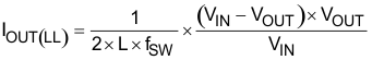
As the output current decreases from heavy-load condition, the inductor current also decreases until the rippled valley of the inductor current touches zero level. Zero level is the boundary between the continuous-conduction and discontinuous-conduction modes. The synchronous MOSFET turns off when this zero inductor current is detected. As the load current decreases further, the converter runs into discontinuous-conduction mode (DCM). The on-time is maintained to a level approximately the same as during continuous-conduction mode operation so that discharging the output capacitor with a smaller load current to the level of the reference voltage requires more time. The transition point to the light-load operation I O(LL) (for example: the threshold between continuous- and discontinuous-conduction mode) is calculated as shown in Equation 5.
where
- f SW is the PWM switching frequency
TI recommends only using ceramic capacitors for Auto-skip mode.
7.4.2 Forced Continuous-Conduction Mode
When the MODE pin is tied to the PGOOD pin through a resistor, the controller operates in continuous conduction mode (CCM) during light-load conditions. During CCM, the switching frequency maintained to an almost constant level over the entire load range which is suitable for applications requiring tight control of the switching frequency at the cost of lower efficiency.
7.5 Programming
7.5.1 The PMBus General Descriptions
The TPS53915 has seven internal custom user-accessible 8-bit registers. The PMBus interface has been designed for program flexibility, supporting a direct format for write operation. Read operations are supported for both combined format and stop separated format. While there is no auto increment/decrement capability in the TPS53915 PMBus logic, a tight software loop can be designed to randomly access the next register, regardless of which register was accessed first. The START and STOP commands frame the data packet and the REPEAT START condition is allowed when necessary.
The device can operate in either standard mode (100 kb/s) or fast mode (400 kb/s).
7.5.2 PMBus Slave Address Selection
The seven-bit slave address is 001A3A2A1A0x, where A3A2A1A0 is set by the ADDR pin on the device. Bit 0 is the data direction bit, i.e., 001A3A2A1A00 is used for write operation and 001A3A2A1A01 is used for read operation.
7.5.3 PMBus Address Selection
The TPS53915 allows up to 16 different chip addresses for PMBus communication, with the first three bits fixed as 001. The address selection process is defined by the resistor divider ratio from VREG pin to ADDR pin, and the address detection circuit starts to work only after VDD input supply has risen above its UVLO threshold. The table below lists the divider ratio and some example resistor values. The 1% tolerance resistors with typical temperature coefficient of ±100 ppm/°C are recommended. Higher performance resistors can be used if tighter noise margin is required for more reliable address detection, as shown in Table 4.
Table 4. PMBus Address Selection Settings
| PMBus ADDRESS | RESISTOR DIVIDER RATIO (Ω) | (RHIGH) (kΩ) HIGH-SIDE RESISTOR |
(RLOW) (kΩ) LOW-SIDE RESISTOR |
||
|---|---|---|---|---|---|
| (RLOW/RLOW+RHIGH) | MIN | MAX | |||
0011111 |
> 0.557 | 1 | 300 | ||
0011110 |
0.5100 | 0.4958 | 0.5247 | 160 | 165 |
0011101 |
0.4625 | 04482 | 0.4772 | 180 | 154 |
0011100 |
0.4182 | 0.4073 | 0.4294 | 200 | 143 |
0011011 |
0.3772 | 0.3662 | 0.3886 | 200 | 120 |
0011010 |
0.3361 | 0.3249 | 0.3476 | 220 | 110 |
0011001 |
0.2985 | 0.2905 | 0.3067 | 249 | 105 |
0011000 |
0.2641 | 0.2560 | 0.2725 | 249 | 88.7 |
0010111 |
0.2298 | 0.2215 | 0.2385 | 240 | 71.5 |
0010110 |
0.1955 | 0.1870 | 0.2044 | 249 | 60.4 |
0010101 |
0.1611 | 0.1524 | 0.1703 | 249 | 47.5 |
0010100 |
0.1268 | 0.1179 | 0.1363 | 249 | 36.0 |
0010011 |
0.0960 | 0.0900 | 0.1024 | 255 | 27.0 |
0010010 |
0.0684 | 0.0622 | 0.0752 | 255 | 18.7 |
0010001 |
0.0404 | 0.0340 | 0.0480 | 270 | 11.5 |
0010000 |
< 0.013 | 300 | 1 | ||
7.5.4 Supported Formats
The supported formats are described in this section.
7.5.4.1 Direct Format: Write
The simplest format for a PMBus write is direct format. After the START condition [S], the slave chip address is sent, followed by an eighth bit indicating a write. The TPS53915 then acknowledges that it is being addressed, and the master responds with an 8-bit register address byte. The slave acknowledges and the master sends the appropriate 8-bit data byte. Again the slave acknowledges and the master terminates the transfer with the STOP condition [P].
7.5.4.2 Combined Format: Read
After the START condition [S], the slave chip address is sent, followed by an eighth bit indicating a write. The TPS53915 then acknowledges that it is being addressed, and the master responds with an 8-bit register address byte. The slave acknowledges and the master sends the repeated START condition [Sr]. Again the slave chip address is sent, followed by an eighth bit indicating a read. The slave responds with an acknowledge followed by previously addressed 8 bit data byte. The master then sends a non-acknowledge (NACK) and finally terminates the transfer with the STOP condition [P].
7.5.4.3 Stop-Separated Reads
Stop-separated read features are also available. This format allows a master to initialize the register address pointer for a read and return to that slave at a later time to read the data. In this format the slave chip address followed by a write bit are sent after a START [S] condition. The TPS53915 then acknowledges it is being addressed, and the master responds with the 8-bit register address byte. The master then sends a STOP or RESTART condition and may then address another slave. After performing other tasks, the master can send a START or RESTART condition to the device with a read command. The device acknowledges this request and returns the data from the register location that had been set up previously.
7.5.5 Supported PMBus Commands
The TPS53915 supports the PMBus commands shown in Table 5 only. Not all features of each PMBus command are supported. The CLEAR_FAULTS, STORE_DEFAULT_ALL and RESTORE_DEFAULT_ALL commands have no data bytes. The non-volatile memory (NVM) cells inside the TPS53915 can permanently store some registers.
Table 5. Supported PMBus Commands
| COMMAND | NOTES |
|---|---|
| OPERATION | Turn on or turn off switching converter only |
| ON_OFF_CONFIG | ON/OFF configuration |
| CLEAR_FAULTS | Clear all latched status flags |
| WRITE_PROTECT | Control writing to the PMBus device |
| STORE_DEFAULT_ALL | Store contents of user-accessible registers to non-volatile memory cells |
| RESTORE_DEFAULT_ALL | Copy contents of non-volatile memory cells to user-accessible registers |
| STATUS_WORD | PMBus read-only status and flag bits |
| CUSTOM_REG | MFR_SPECIFIC_00 (Custom Register 0): Custom register |
| DELAY_CONTROL | MFR_SPECIFIC_01 (Custom Register 1): Power on and power good delay times |
| MODE_SOFT_START_CONFIG | MFR_SPECIFIC_02 (Custom Register 2): Mode and soft-start time |
| FREQUENCY_CONFIG | MFR_SPECIFIC_03 (Custom Register 3): Switching frequency control |
| VOUT_ADJUSTMENT | MFR_SPECIFIC_04 (Custom Register 4): Output voltage adjustment control |
| VOUT_MARGIN | MFR_SPECIFIC_05 (Custom Register 5): Output voltage margin levels |
| UVLO_THRESHOLD | MFR_SPECIFIC_06 (Custom Register 6): Turn-on input voltage UVLO threshold |
7.5.5.1 Unsupported PMBus Commands
Do not send any unsupported commands to the TPS53915. Even though the device receives an unsupported commands, it can acknowledge the unsupported commands and any related data bytes by properly sending the ACK bits. However, the device ignores the unsupported commands and any related data bytes, which means they do not affect the device operation in any way. Although the TPS53915 may acknowledge but ignore unsupported commands and data bytes, it can however, set the CML bit in the STATUS_BYTE register and then pull down the ALERT pin to notify the host. For this reason, unsupported commands and data bytes should not be sent to TPS53915.
7.5.5.2 OPERATION [01h] (R/W Byte)
The TPS53915 supports only the functions of the OPERATION command shown in Table 6.
Table 6. OPERATION Command Supported Functions
| COMMAND | DEFINITION | DESCRIPTION | NVM | |
|---|---|---|---|---|
| OPERATION<7> | ON_OFF | 0: turn off switching converter 1: turn on switching converter |
— | |
| OPERATION<6> | — | not supported and don’t care | — | |
| OPERATION<5:2> | OPMARGIN<3:0> | 00xx: turn off output voltage margin function 0101: turn on output voltage margin low and ignore fault 0110: turn on output voltage margin low and act on fault 1001: turn on output voltage margin high and ignore fault 1010: turn on output voltage margin high and act on fault |
— | |
| OPERATION<1> | — | not supported and don’t care | — | |
| OPERATION<0> | — | not supported and don’t care | — | |
7.5.5.3 ON_OFF_CONFIG [02h] (R/W Byte)
The TPS53915 supports only the functions of the ON_OFF_CONFIG command shown in Table 7.
Table 7. ON_OFF_CONFIG Command Supported Functions
| COMMAND | DEFINITION | DESCRIPTION | NVM | |
|---|---|---|---|---|
| ON_OFF_CONFIG<7> | — | not supported and don’t care | — | |
| ON_OFF_CONFIG<6> | — | not supported and don’t care | — | |
| ON_OFF_CONFIG<5> | — | not supported and don’t care | — | |
| ON_OFF_CONFIG<4> | PU | not supported and always set to 1 | — | |
| ON_OFF_CONFIG<3> | CMD | 0: ignore ON_OFF bit (OPERATION<7>)(1)
1: act on ON_OFF bit (OPERATION<7>) |
Yes | |
| ON_OFF_CONFIG<2> | CP | 0: ignore EN pin 1: act on EN pin(1) |
Yes | |
| ON_OFF_CONFIG<1> | PL | not supported and always set to 1 | — | |
| ON_OFF_CONFIG<0> | SP | not supported and always set to 1 | — | |
Conditions required to enable the switcher:
- If CMD is cleared and CP is set, then the switcher can be enabled only by the EN pin.
- If CMD is set and CP is cleared, then the switcher can be enabled only by the ON_OFF bit (OPERATION<7>) via PMBus.
- If both CMD and CP are set, then the switcher can be enabled only when both the ON_OFF bit (OPERATION<7>) and the EN pin are commanding to enable the device.
- If both CMD and CP are cleared, then the switcher is automatically enabled after the ADDR detection sequence completes, regardless of EN pin and ON_OFF bit polarities.
7.5.5.4 WRITE_PROTECT [10h] (R/W Byte)
The WRITE PROTECT command is used to control writing to the PMBus device. The intent of this command is to provide protection against accidental changes. This command has one data byte as described in Table 8.
Table 8. WRITE_PROTECT Command Supported Functions
| COMMAND | DEFINITION | DESCRIPTION | NVM | |
|---|---|---|---|---|
| WRITE_PROTECT<7:0> | WP<7:0> | 10000000: |
Disable all writes, except the WRITE_PROTECT command. | — |
01000000: |
Disable all writes, except the WRITE_PROTECT and OPERATION commands. | — | ||
00100000: |
Disable all writes, except the WRITE_PROTECT, OPERATION, and ON_OFF_CONFIG commands. | — | ||
00000000: |
Enable writes to all commands. | — | ||
Others: |
Fault data | — | ||
7.5.6 CLEAR_FAULTS [03h] (Send Byte)
The CLEAR_FAULTS command is used to clear any fault bits in the STATUS_WORD and STATUS_BYTE registers that have been set. This command clears all bits in all status registers. Simultaneously, the TPS53915 releases its ALERT signal output if the device is asserting the ALERT signal. If the FAULT condition is still present when the bit is cleared, the fault bits shall immediately be set again, and the ALERT signal should also be re-asserted.
The CLEAR_FAULTS does not cause a unit that has latched off for a FAULT condition to restart. Units that have been shut down for a FAULT condition can be restarted with one of the following conditions.
- The output is commanded through the EN pin and/or ON_OFF bit based on the ON_OFF_CONFIG setting to turn off and then to turn back on.
- VDD power is cycled for TPS53915
The CLEAR_FAULT command is used to clear the fault bits in the STATUS_WORD and STATUS_BYTE commands, and to release the ALERT pin. It is recommended not to send CLEAR_FAULT command when there is no fault to cause the ALERT pin to pull down.
7.5.7 STORE_DEFAULT_ALL [11h] (Send Byte)
The STORE_DEFAULT_ALL command instructs TPS53915 to copy the entire contents of the operating memory to the corresponding locations in the NVM. The updated contents in the non-volitile memory (NVM)s become the new default values. The STORE_DEFAULT_ALL command can be used while the device is operating. However, the device may be unresponsive during the copy operation with unpredictable results. (see PMBus Power System Management Protocol Specificaiton, Part II - Command Language, Revision, 1.2, 6 Sept. 2010. www.powerSIG.org). It is recommended not to exceed 1000 write/erase cycles for non-volatile memory (NVM).
7.5.8 RESTORE_DEFAULT_ALL [12h] (Send Byte)
The RESTORE_DEFAULT_ALL command instructs TPS53915 to copy the entire contents of the NVMs to the corresponding locations in the operating memory. The values in the operating memory are overwritten by the value retrieved from the NVM. It is permitted to use the RESTORE_DEFAULT_ALL command while the device is operating. However, the device may be unresponsive during the copy operation with unpredictable results.
7.5.9 STATUS_WORD [79h] (Read Word)
The TPS53915 does not support all functions of the STATUS_WORD command. A list of supported functions appears in Table 9. A status bit reflects the current state of the converter. Status bit becomes high when the specified condition has occurred and goes low when the specified condition has disappeared. A flag bit is a latched bit that becomes high when the specified condition has occurred and does not go back low when the specified condition has disappeared. STATUS_BYTE command is a subset of the STATUS_WORD command, or more specifically the lower byte of the STATUS_WORD.
Table 9. STATUS_WORD Command Supported Functions
| COMMAND | DEFINITION | DESCRIPTION |
|---|---|---|
| Low Byte: STATUS_BYTE [78h] | ||
| Low STATUS_WORD<7> | BUSY | not supported and always set to 0 |
| Low STATUS_WORD<6> | OFF | 0: raw status indicating device is providing power to output voltage 1: raw status indicating device is not providing power to output voltage |
| Low STATUS_WORD<5> | VOUT_OV | 0: latched flag indicating no output voltage overvoltage fault has occurred 1: latched flag indicating an output voltage overvoltage fault has occurred |
| Low STATUS_WORD<4> | IOUT_OC | 0: latched flag indicating no output current overcurrent fault has occurred 1: latched flag indicating an output current overcurrent fault has occurred |
| Low STATUS_WORD<3> | VIN_UV | 0: latched flag indicating input voltage is above the UVLO turn-on threshold 1: latched flag indicating input voltage is below the UVLO turn-on threshold |
| Low STATUS_WORD<2> | TEMP | 0: latched flag indicating no OT fault has occurred 1: latched flag indicating an OT fault has occurred |
| Low STATUS_WORD<1> | CML | 0: latched flag indicating no communication, memory or logic fault has occurred 1: latched flag indicating a communication, memory or logic fault has occurred |
| Low STATUS_WORD<0> | OTHER | not supported and always set to 0 |
| High Byte | ||
| High STATUS_WORD<7> | VOUT | 0: latched flag indicating no output voltage fault or warning has occurred 1: latched flag indicating a output voltage fault or warning has occurred |
| High STATUS_WORD<6> | IOUT | 0: latched flag indicating no output current fault or warning has occurred 1: latched flag indicating an output current fault or warning has occurred |
| High STATUS_WORD<5> | INPUT | 0: latched flag indicating no input voltage fault or warning has occurred 1: latched flag indicating a input voltage fault or warning has occurred |
| High STATUS_WORD<4> | MFR | not supported and always set to 0 |
| High STATUS_WORD<3> | PGOOD | 0: raw status indicating PGOOD pin is at logic high 1: raw status indicating PGOOD pin is at logic low |
| High STATUS_WORD<2> | FANS | not supported and always set to 0 |
| High STATUS_WORD<1> | OTHER | not supported and always set to 0 |
| High STATUS_WORD<0> | UNKNOWN | not supported and always set to 0 |
The latched flags of faults can be removed or corrected only until one of the following conditions occurs:
- The device receives a CLEAR_FAULTS command.
- The output is commanded through the EN pin and/or ON_OFF bit based on the ON_OFF_CONFIG setting to turn off and then to turn back on
- VDD power is cycled for TPS53915
If the FAULT condition remains present when the bit is cleared, the fault bits are immediately set again, and the ALERT signal is re-asserted.
TPS53915 supports the ALERT pin to notify the host of FAULT conditions. Therefore, the best practice for monitoring the fault conditions from the host is to treat the ALERT pin as an interrupt source for triggering the corresponding interrupt service routine. It is recommended not to keep polling the STATUS_WORD or STATUS_BYTE registers from the host to reduce the firmware overhead of the host.
7.5.10 CUSTOM_REG (MFR_SPECIFIC_00) [D0h] (R/W Byte)
Custom register 0 provides the flexibility for users to store any desired non-volatile information. For example, users can program this register to track versions of implementation or other soft identification information. The details of each setting are listed in Table 10.
Table 10. CUSTOM_REG (MFR_SPECIFIC_00) Settings
| COMMAND | DEFINITION | DESCRIPTION | NVM |
|---|---|---|---|
| CUSTOM_REG<7> | — | not supported and don’t care | — |
| CUSTOM_REG<6> | — | not supported and don’t care | — |
| CUSTOM_REG<5:0> | CUSTOMWORD <5:0> | 00000:(1) can be used to store any desired non-volatile information. | Yes |
7.5.11 DELAY_CONTROL (MFR_SPECIFIC_01) [D1h] (R/W Byte)
Custom register 1 provides software control over key timing parameters of the controller: Power-on delay (POD) time and power-good delay (PGD) time. The details of each setting are listed in Table 11.
Table 11. DELAY_CONTROL (MFR_SPECIFIC_01) Settings
| COMMAND | DEFINITION | DESCRIPTION | NVM |
|---|---|---|---|
| DELAY_CONTROL<7> | — | not supported and don’t care | — |
| DELAY_CONTROL<6> | — | not supported and don’t care | — |
| DELAY_CONTROL<5:3> | PGD<2:0> | 000: 256 µs 001: 512 µs 010: 1.024 ms(1) 011: 2.048 ms 100: 4.096 ms 101: 8.192 ms 110: 16.384 ms 111: 131.072 ms |
Yes |
| DELAY_CONTROL<2:0> | POD<2:0> | 000: 356 µs 001: 612 µs 010: 1.124 ms(1) 011: 2.148 ms 100: 4.196 ms 101: 8.292 ms 110: 16.484 ms 111: 32.868 ms |
Yes |
7.5.12 MODE_SOFT_START_CONFIG (MFR_SPECIFIC_02) [D2h] (R/W Byte)
Custom register 2 provides software control over mode selection and soft-start time (tSS). The details of each setting are listed in Table 12.
Table 12. MODE_SOFT_START_CONFIG (MFR_SPECIFIC_02) Settings
| COMMAND | DEFINITION | DESCRIPTION | NVM |
|---|---|---|---|
| MODE_SOFT_START_CONFIG<7> | — | not supported and don’t care | — |
| MODE_SOFT_START_CONFIG<6> | — | not supported and don’t care | — |
| MODE_SOFT_START_CONFIG<5> | — | not supported and don’t care | — |
| MODE_SOFT_START_CONFIG<4> | — | not supported and don’t care | — |
| MODE_SOFT_START_CONFIG<3:2> | SST<1:0> | 00: 1 ms(1)
01: 2 ms 10: 4 ms 11: 8 ms |
Yes |
| MODE_SOFT_START_CONFIG<1> | HICLOFF | 0: hiccup after UV(1)
Hiccup interval is (8.96 ms + soft-start time × 7) 1: latch-off after UV |
Yes |
| MODE_SOFT_START_CONFIG<0> | CM | 0: DCM(1)
1: FCCM |
Yes |
Figure 48 shows the soft-start timing diagram of TPS53915 with the programmable power-on delay time (tPOD), soft-start time (tSST), and PGOOD delay time (tPGD). During the soft-start time, the controller remains in discontinuous conduction mode (DCM), and then switches to forced continuous conduction mode (FCCM) at the end of soft-start if CM bit (MODE_SOFT_START_CONFIG<0>) is set.
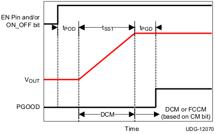 Figure 48. Programmable Soft-Start Timing
7.5.13 FREQUENCY_CONFIG (MFR_SPECIFIC_03) [D3h] (R/W Byte)
Custom register 3 provides software control over frequency setting (FS). The details of FS setting are listed in Table 13.
Table 13. FREQUENCY_CONFIG (MFR_SPECIFIC_03) Settings
| COMMAND | DEFINITION | DESCRIPTION | NVM |
|---|---|---|---|
| FREQUENCY_CONFIG<7> | — | not supported and don’t care | — |
| FREQUENCY_CONFIG<6> | — | not supported and don’t care | — |
| FREQUENCY_CONFIG<5> | — | not supported and don’t care | — |
| FREQUENCY_CONFIG<4> | — | not supported and don’t care | — |
| FREQUENCY_CONFIG<3> | — | not supported and don’t care | — |
| FREQUENCY_CONFIG<2:0> | FS<2:0> | 000: 250 kHz 001: 300 kHz 010: 400 kHz (1) 011: 500 kHz 100: 600 kHz 101: 750 kHz 110: 850 kHz 111: 1 MHz |
Yes |
7.5.14 VOUT_ADJUSTMENT (MFR_SPECIFIC_04) [D4h] (R/W Byte)
Custom register 4 provides ouput voltage adjustment (VOA) in ±0.75% steps, with a total range of ±9%. When fine adjustment is used together with the margin setting, the change in the output voltage is determined by the multiplication of the two settings.
Table 14. VOUT_ADJUSTMENT (MFR_SPECIFIC_04) Settings
| COMMAND | DEFINITION | DESCRIPTION | NVM |
|---|---|---|---|
| VOUT_ADJUSTMENT<7> | — | not supported and don’t care | — |
| VOUT_ADJUSTMENT<6> | — | not supported and don’t care | — |
| VOUT_ADJUSTMENT<5> | — | not supported and don’t care | — |
| VOUT_ADJUSTMENT<4:0> | VOA<4:0> | 111xx: +9.00% 11011: +8.25% 11010: +7.50% 11001: +6.75% 11000: +6.00% 10111: +5.25% 10110: +4.50% 10101: +3.75% 10100: +3.00% 10011: +2.25% 10010: +1.50% 10001: +0.75% 10000: +0%(1) 01111: –0% 01110: –0.75% 01101: –1.50% 01100: –2.25% 01011: –3.00% 01010: –3.75% 01001: –4.50% 01000: –5.25% 00111: –6.00% 00110: –6.75% 00101: –7.50% 00100: –8.25% 000xx: –9.00% |
Yes |
7.5.15 Output Voltage Fine Adjustment Soft Slew Rate
To prevent sudden buildup of voltage across inductor, output voltage fine adjustment setting cannot change output voltage instantaneously. The internal reference voltage must slew slowly to its final target, and SST<1:0> is used to provide further programmability. The details of output voltage fine adjustment slew rate are shown in Table 15.
Table 15. Output Voltage Fine Adjustment Soft Slew Rate Settings
| COMMAND | DEFINITION | DESCRIPTION | NVM |
|---|---|---|---|
| MODE_SOFT_START_CONFIG<3:2> | SST<1:0> | 00: 1 step per 4 µs(1)
01: 1 step per 8 µs 10: 1 step per 16 µs 11: 1 step per 32 µs |
Yes |
7.5.16 VOUT_MARGIN (MFR_SPECIFIC_05) [D5h] (R/W Byte)
Custom register 5 provides output voltage margin high (VOMH) and output voltage margin low (VOML) settings. This register works in conjunction with PMBus OPERATION command to raise or lower the output voltage by a specified amount. This register settings described in Table 16 are also used together with the fine adjustment setting described in Table 14. For example, setting fine adjustment to +9% and margin to +12% changes the output by +22.08%, whereas setting fine adjustment to –9% and margin to –9% change the output by –17.19%
Table 16. VOUT_MARGIN (MFR_SPECIFIC_05) Settings
| COMMAND | DEFINITION | DESCRIPTION | NVM |
|---|---|---|---|
| VOUT_MARGIN<7:4> | VOMH<3:0> | 11xx: +12.0% 1011: +10.9% 1010: +9.9% 1001: +8.8% 1000: +7.7% 0111: +6.7% 0110: +5.7% 0101: +4.7%(1) 0100: +3.7% 0011: +2.8% 0010: +1.8% 0001: +0.9% 0000: +0% |
Yes |
| VOUT_MARGIN<3:0> | VOML<3:0> | 0000: –0% 0001: –1.1% 0010: –2.1% 0011: –3.2% 0100: –4.2% 0101: –5.2% (1) 0110: –6.2% 0111: –7.1% 1000: –8.1% 1001: –9.0% 1010: –9.9% 1011: –10.7% 11xx: –11.6% |
Yes |
7.5.17 Output Voltage Margin Adjustment Soft-Slew Rate
Similar to the output voltage fine adjustment, margin adjustment also cannot change output voltage instantaneously. The soft-slew rate of margin adjustment is also programmed by SST<1:0>. The details are listed in Table 17.
Table 17. Output Voltage Margin Adjustment Soft-Slew Rate Settings
| COMMAND | DEFINITION | DESCRIPTION | NVM |
|---|---|---|---|
| MODE_SOFT_START_CONFIG<3:2> | SST<1:0> | 00: 1 step per 4 µs(1)
01: 1 step per 8 µs 10: 1 step per 16 µs 11: 1 step per 32 µs |
Yes |
Figure 49 shows the timing diagram of the output voltage adjustment via PMBus. After receiving the write command of VOUT_ADJUSTMENT (MFR_SPECIFIC_04), the output voltage starts to be adjusted after tP delay time (about 50 μs). The time duration tDAC for each DAC step change can be controlled by SST bits (MODE_SOFT_START_CONFIG<3:2:> from 4 μs to 32 μs.
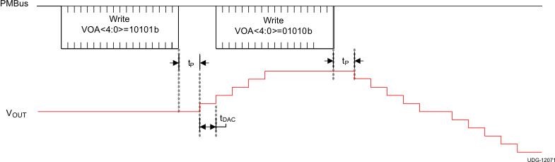 Figure 49. Output Voltage Adjustment via PMBus
The margining function is enabled by setting the OPERATION command, and the margining level is determined by the VOUT_MARGIN (MFR_SPECIFIC_05) command. Figure 50 and Figure 51 illustrate the timing diagrams of the output voltage margining via PMBus. Figure 50 shows setting the margining level first, and then enabling margining by writing OPERATION command. After the OPERATION margin high command enables the margin high setting (VOMH<3:0>), the output voltage starts to be adjusted after tP delay time (about 50 μs). The time duration tDAC for each DAC step change can be controlled by SST bits (MODE_SOFT_START_CONFIG<3:2>) from 4 μs to 32 μs.
As shown in Figure 51, the margining function is enabled first by a write command of OPERATION. The output voltage starts to be adjusted toward the default margin high level after tP delay. Because the margining function has been enabled, the output voltage can be adjusted again by sending a different margin high level with a write command of VOUT_MARGIN. The time duration tDAC for each DAC step change can be also controlled by SST bits (MODE_SOFT_START_CONFIG<3:2>) from 4 μs to 32 μs.
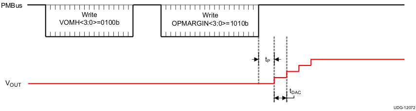 Figure 50. Setting the Margining Level First
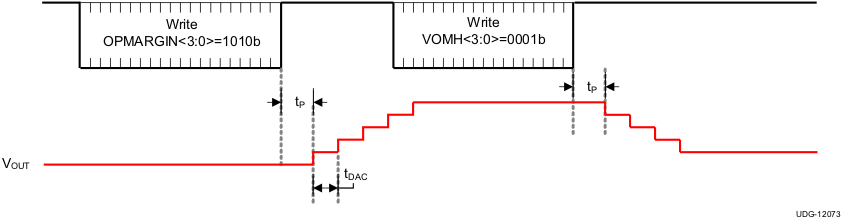 Figure 51. Enabling Margining First
7.5.18 UVLO_THRESHOLD (MFR_SPECIFIC_06) [D6h]
Custom register 6 provides some limited programmability of input supply UVLO threshold, as described in Table 18. The default turn-on UVLO threshold is 4.25 V.
Table 18. UVLO_THRESHOLD (MFR_SPECIFIC_06) Settings
| COMMAND | DEFINITION | DESCRIPTION | NVM |
|---|---|---|---|
| UVLO_THRESHOLD<7> | — | not supported and don’t care | — |
| UVLO_THRESHOLD<6> | — | not supported and don’t care | — |
| UVLO_THRESHOLD<5> | — | not supported and don’t care | — |
| UVLO_THRESHOLD<4> | — | not supported and don’t care | — |
| UVLO_THRESHOLD<3> | — | not supported and don’t care | — |
| UVLO_THRESHOLD<2:0> | VDDINUVLO<2:0> | 0xx: 10.2 V 100: not supported and should not be used 101: 4.25 V(1) 110: 6.0 V 111: 8.1 V |
Yes |