SLUSAS9B NOVEMBER 2013 – December 2014 TPS53915
PRODUCTION DATA.
- 1 Features
- 2 Applications
- 3 Description
- 4 Revision History
- 5 Pin Configuration and Functions
- 6 Specifications
-
7 Detailed Description
- 7.1 Overview
- 7.2 Functional Block Diagrams
- 7.3
Feature Description
- 7.3.1 Powergood
- 7.3.2 D-CAP3 Control and Mode Selection
- 7.3.3 D-CAP3 Mode
- 7.3.4 Sample and Hold Circuitry
- 7.3.5 Adaptive Zero-Crossing
- 7.3.6 Forced Continuous-Conduction Mode
- 7.3.7 Current Sense and Overcurrent Protection
- 7.3.8 Overvoltage and Undervoltage Protection
- 7.3.9 Out-Of-Bounds Operation (OOB)
- 7.3.10 UVLO Protection
- 7.3.11 Thermal Shutdown
- 7.4 Device Functional Modes
- 7.5
Programming
- 7.5.1 The PMBus General Descriptions
- 7.5.2 PMBus Slave Address Selection
- 7.5.3 PMBus Address Selection
- 7.5.4 Supported Formats
- 7.5.5 Supported PMBus Commands
- 7.5.6 CLEAR_FAULTS [03h] (Send Byte)
- 7.5.7 STORE_DEFAULT_ALL [11h] (Send Byte)
- 7.5.8 RESTORE_DEFAULT_ALL [12h] (Send Byte)
- 7.5.9 STATUS_WORD [79h] (Read Word)
- 7.5.10 CUSTOM_REG (MFR_SPECIFIC_00) [D0h] (R/W Byte)
- 7.5.11 DELAY_CONTROL (MFR_SPECIFIC_01) [D1h] (R/W Byte)
- 7.5.12 MODE_SOFT_START_CONFIG (MFR_SPECIFIC_02) [D2h] (R/W Byte)
- 7.5.13 FREQUENCY_CONFIG (MFR_SPECIFIC_03) [D3h] (R/W Byte)
- 7.5.14 VOUT_ADJUSTMENT (MFR_SPECIFIC_04) [D4h] (R/W Byte)
- 7.5.15 Output Voltage Fine Adjustment Soft Slew Rate
- 7.5.16 VOUT_MARGIN (MFR_SPECIFIC_05) [D5h] (R/W Byte)
- 7.5.17 Output Voltage Margin Adjustment Soft-Slew Rate
- 7.5.18 UVLO_THRESHOLD (MFR_SPECIFIC_06) [D6h]
- 8 Application and Implementation
- 9 Power Supply Recommendations
- 10Layout
- 11Device and Documentation Support
- 12Mechanical, Packaging, and Orderable Information
パッケージ・オプション
メカニカル・データ(パッケージ|ピン)
- RVE|28
サーマルパッド・メカニカル・データ
- RVE|28
発注情報
10 Layout
10.1 Layout Guidelines
Before beginning a design using the TPS53915, consider the following:
- Place the power components (including input and output capacitors, the inductor, and the TPS53915) on the solder side of the PCB. In order to shield and isolate the small signal traces from noisy power lines, insert and connect at least one inner plane to ground.
- All sensitive analog traces and components such as VFB, PGOOD, TRIP, MODE, and ADDR must be placed away from high-voltage switching nodes such as SW and VBST to avoid coupling. Use internal layers as ground planes and shield the feedback trace from power traces and components.
- Pin 22 (GND pin) must be connected directly to the thermal pad. Connect the thermal pad to the PGND pins and then to the GND plane.
- Place the VIN decoupling capacitors as close to the VIN and PGND pins as possible to minimize the input AC-current loop.
- Place the feedback resistor near the IC to minimize the VFB trace distance.
- Place the frequency-setting resistor (ADDR), OCP-setting resistor (RTRIP) and mode-setting resistor (RMODE) close to the device. Use the common GND via to connect the resistors to the GND plane if applicable.
- Place the VDD and VREG decoupling capacitors as close to the device as possible. Provide GND vias for each decoupling capacitor and ensure the loop is as small as possible.
- The PCB trace is defined as switch node, which connects the SW pins and high-voltage side of the inductor. The switch node should be as short and wide as possible.
- Use separated vias or trace to connect SW node to the snubber, bootstrap capacitor, and ripple-injection resistor. Do not combine these connections.
- Place one more small capacitor (2.2 nF- 0402 size) between the VIN and PGND pins. This capacitor must be placed as close to the IC as possible.
- TI recommends placing a snubber between the SW shape and GND shape for effective ringing reduction. The value of snubber design starts at 3 Ω + 470 pF.
- Consider R,C,Cc network (Ripple injection network) component placement and place the AC coupling capacitor, Cc, close to the device, and R and C close to the power stage.
- See Figure 65 for the layout recommendation.
10.2 Layout Example
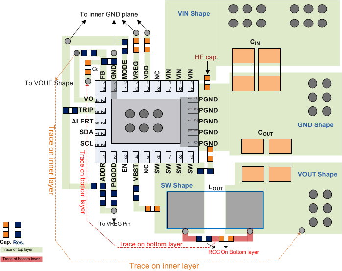 Figure 65. Layout Recommendation