SLVSBZ2A September 2013 – November 2014 TPS54360-Q1
PRODUCTION DATA.
- 1 Features
- 2 Applications
- 3 Description
- 4 Revision History
- 5 Pin Configuration and Functions
- 6 Specifications
-
7 Detailed Description
- 7.1 Overview
- 7.2 Functional Block Diagram
- 7.3
Feature Description
- 7.3.1 Fixed Frequency PWM Control
- 7.3.2 Slope Compensation Output Current
- 7.3.3 Pulse Skip Eco-Mode™
- 7.3.4 Low Dropout Operation and Bootstrap Voltage (BOOT)
- 7.3.5 Error Amplifier
- 7.3.6 Adjusting the Output Voltage
- 7.3.7 Enable and Adjusting Undervoltage Lockout
- 7.3.8 Internal Soft-Start
- 7.3.9 Constant Switching Frequency and Timing Resistor (RT/CLK) Pin)
- 7.3.10 Accurate Current Limit Operation and Maximum Switching Frequency
- 7.3.11 Synchronization to RT/CLK Pin
- 7.3.12 Overvoltage Protection
- 7.3.13 Thermal Shutdown
- 7.3.14 Small Signal Model for Loop Response
- 7.3.15 Simple Small Signal Model for Peak Current Mode Control
- 7.3.16 Small Signal Model for Frequency Compensation
- 7.4 Device Functional Modes
-
8 Application and Implementation
- 8.1 Application Information
- 8.2
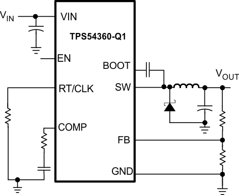
Typical Application
- 8.2.1
5-V Output TPS54360-Q1 Design Example
- 8.2.1.1 Design Requirements
- 8.2.1.2
Detailed Design Procedure
- 8.2.1.2.1 Selecting the Switching Frequency
- 8.2.1.2.2 Output Inductor Selection (LO)
- 8.2.1.2.3 Output Capacitor
- 8.2.1.2.4 Catch Diode
- 8.2.1.2.5 Input Capacitor
- 8.2.1.2.6 Bootstrap Capacitor Selection
- 8.2.1.2.7 Undervoltage Lockout Set Point
- 8.2.1.2.8 Output Voltage and Feedback Resistors Selection
- 8.2.1.2.9 Compensation
- 8.2.1.2.10 Discontinuous Conduction Mode and Eco-Mode™ Boundary
- 8.2.1.2.11 Power Dissipation Estimate
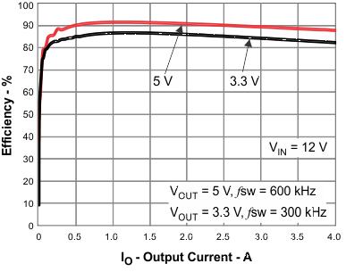
- 8.2.1.3 Application Curves
- 8.2.2 TPS54360-Q1 Inverting Power Supply
- 8.2.3 TPS54360-Q1 Split Rail Power Supply
- 8.2.1
5-V Output TPS54360-Q1 Design Example
- 9 Power Supply Recommendations
- 10Layout
- 11Device and Documentation Support
- 12Mechanical, Packaging, and Orderable Information
パッケージ・オプション
メカニカル・データ(パッケージ|ピン)
- DDA|8
サーマルパッド・メカニカル・データ
- DDA|8
発注情報
1 Features
- Qualified for Automotive Applications
- AEC-Q100 Qualified With the Following Results:
- Device Temperature Grade 1: –40°C to 125°C Ambient Operating Temperature Range
- Device HBM ESD Classification Level H1C
- Device CDM ESD Classification Level C3B
- High Efficiency at Light Loads With Pulse Skipping Eco-Mode™
- 92-mΩ High-Side MOSFET
- 146-μA Operating Quiescent Current and 2 µA Shutdown Current
- 100-kHz to 2.5-MHz Adjustable Switching Frequency
- Synchronizes to External Clock
- Low Dropout at Light Loads With Integrated BOOT Recharge FET
- Adjustable UVLO Voltage and Hysteresis
- 0.8-V 1% Internal Voltage Reference
- 8-Pin SO With PowerPAD™ Package
- –40°C to 150°C TJ Operating Range
- Supported by WEBENCH® Software Tool
2 Applications
3 Description
The TPS54360-Q1 is a 60-V 3.5-A step-down regulator with an integrated high-side MOSFET. The device survives load dump pulses up to 65 V per ISO 7637. Current mode control provides simple external compensation and flexible component selection. A low-ripple pulse-skip mode reduces the no-load supply current to 146 μA. Shutdown supply current is reduced to 2 μA when the enable pin is pulled low.
Undervoltage lockout is internally set at 4.3 V but can be increased using an external resistor divider at the enable pin. The output voltage start-up ramp is internally controlled to provide a controlled start up and eliminate overshoot.
A wide adjustable frequency range allows either efficiency or external component size to be optimized. Frequency foldback and thermal shutdown protects internal and external components during an overload condition.
The TPS54360-Q1 is available in an 8-pin thermally enhanced HSOIC PowerPAD package.
Device Information(1)
| PART NUMBER | PACKAGE | BODY SIZE (NOM) |
|---|---|---|
| TPS54360-Q1 | SO PowerPAD (8) | 4.89 mm x 3.90 mm |
- For all available packages, see the orderable addendum at the end of the datasheet.
Simplified Schematic
Efficiency vs Load Current