SLVSBZ2A September 2013 – November 2014 TPS54360-Q1
PRODUCTION DATA.
- 1 Features
- 2 Applications
- 3 Description
- 4 Revision History
- 5 Pin Configuration and Functions
- 6 Specifications
-
7 Detailed Description
- 7.1 Overview
- 7.2 Functional Block Diagram
- 7.3
Feature Description
- 7.3.1 Fixed Frequency PWM Control
- 7.3.2 Slope Compensation Output Current
- 7.3.3 Pulse Skip Eco-Mode™
- 7.3.4 Low Dropout Operation and Bootstrap Voltage (BOOT)
- 7.3.5 Error Amplifier
- 7.3.6 Adjusting the Output Voltage
- 7.3.7 Enable and Adjusting Undervoltage Lockout
- 7.3.8 Internal Soft-Start
- 7.3.9 Constant Switching Frequency and Timing Resistor (RT/CLK) Pin)
- 7.3.10 Accurate Current Limit Operation and Maximum Switching Frequency
- 7.3.11 Synchronization to RT/CLK Pin
- 7.3.12 Overvoltage Protection
- 7.3.13 Thermal Shutdown
- 7.3.14 Small Signal Model for Loop Response
- 7.3.15 Simple Small Signal Model for Peak Current Mode Control
- 7.3.16 Small Signal Model for Frequency Compensation
- 7.4 Device Functional Modes
-
8 Application and Implementation
- 8.1 Application Information
- 8.2
Typical Application
- 8.2.1
5-V Output TPS54360-Q1 Design Example
- 8.2.1.1 Design Requirements
- 8.2.1.2
Detailed Design Procedure
- 8.2.1.2.1 Selecting the Switching Frequency
- 8.2.1.2.2 Output Inductor Selection (LO)
- 8.2.1.2.3 Output Capacitor
- 8.2.1.2.4 Catch Diode
- 8.2.1.2.5 Input Capacitor
- 8.2.1.2.6 Bootstrap Capacitor Selection
- 8.2.1.2.7 Undervoltage Lockout Set Point
- 8.2.1.2.8 Output Voltage and Feedback Resistors Selection
- 8.2.1.2.9 Compensation
- 8.2.1.2.10 Discontinuous Conduction Mode and Eco-Mode™ Boundary
- 8.2.1.2.11 Power Dissipation Estimate
- 8.2.1.3 Application Curves
- 8.2.2 TPS54360-Q1 Inverting Power Supply
- 8.2.3 TPS54360-Q1 Split Rail Power Supply
- 8.2.1
5-V Output TPS54360-Q1 Design Example
- 9 Power Supply Recommendations
- 10Layout
- 11Device and Documentation Support
- 12Mechanical, Packaging, and Orderable Information
パッケージ・オプション
メカニカル・データ(パッケージ|ピン)
- DDA|8
サーマルパッド・メカニカル・データ
- DDA|8
発注情報
8 Application and Implementation
NOTE
Information in the following applications sections is not part of the TI component specification, and TI does not warrant its accuracy or completeness. TI’s customers are responsible for determining suitability of components for their purposes. Customers should validate and test their design implementation to confirm system functionality.
8.1 Application Information
The TPS54360-Q1 device is a 60-V, 3.5-A, step down regulator with an integrated high side MOSFET. This device is typically used to convert a higher DC voltage to a lower DC voltage with a maximum available output current of 3.5 A. Example applications are: 12 V, 24 V and 48 V Industrial, Automotive and Communications Power Systems. Use the following design procedure to select component values for the TPS54360-Q1 device. This procedure illustrates the design of a high frequency switching regulator using ceramic output capacitors. Calculations can be done with the excel spreadsheet (SLVC452) located on the product page. Alternately, use the WEBENCH software to generate a complete design. The WEBENCH software uses an iterative design procedure and accesses a comprehensive database of components when generating a design.
8.2 Typical Application
8.2.1 5-V Output TPS54360-Q1 Design Example
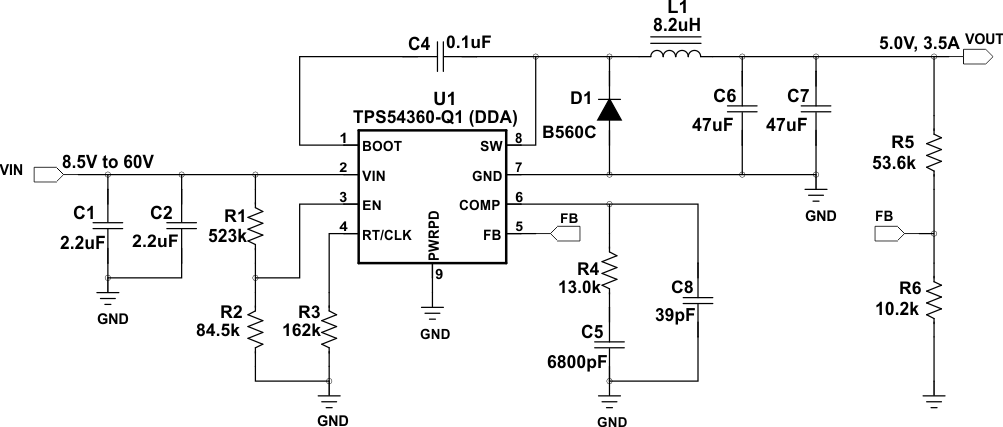 Figure 34. 5 V Output TPS54360-Q1 Design Example
8.2.1.1 Design Requirements
A few parameters must be known in order to start the design process. These requirements are typically determined at the system level. This example is designed to the following known parameters:
| DESIGN PARAMETER | EXAMPLE VALUE |
|---|---|
| Output Voltage | 5 V |
| Transient Response 0.875 A to 2.625 A load step | ΔVOUT = 4 % |
| Maximum Output Current | 3.5 A |
| Input Voltage | 12 V nom. 8.5 V to 60 V |
| Output Voltage Ripple | 0.5% of VOUT |
| Start Input Voltage (rising VIN) | 8 V |
| Stop Input Voltage (falling VIN) | 6.25 V |
8.2.1.2 Detailed Design Procedure
8.2.1.2.1 Selecting the Switching Frequency
The first step is to choose a switching frequency for the regulator. Typically, the designer uses the highest switching frequency possible because this produces the smallest solution size. High switching frequency allows for lower value inductors and smaller output capacitors compared to a power supply that switches at a lower frequency. The switching frequency that can be selected is limited by the minimum on-time of the internal power switch, the input voltage, the output voltage and the frequency foldback protection.
Equation 7 and Equation 8 must be used to calculate the upper limit of the switching frequency for the regulator. Choose the lower value result from the two equations. Switching frequencies higher than these values results in pulse skipping or the lack of overcurrent protection during a short circuit.
The typical minimum on time, tonmin, is 135 ns for the TPS54360-Q1. For this example, the output voltage is 5 V and the maximum input voltage is 60 V, which allows for a maximum switch frequency up to 710 kHz to avoid pulse skipping from Equation 7. To ensure overcurrent runaway is not a concern during short circuits use Equation 8 to determine the maximum switching frequency for frequency foldback protection. With a maximum input voltage of 60 V, assuming a diode voltage of 0.7 V, inductor resistance of 25 mΩ, switch resistance of 92 mΩ, a current limit value of 4.7 A and short circuit output voltage of 0.1 V, the maximum switching frequency is 902 kHz.
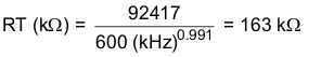
For this design, a lower switching frequency of 600 kHz is chosen to operate comfortably below the calculated maximums. To determine the timing resistance for a given switching frequency, use Equation 5 or the curve in Figure 6. The switching frequency is set by resistor R3 shown in Figure 34. For 600 kHz operation, the closest standard value resistor is 162 kΩ.


8.2.1.2.2 Output Inductor Selection (LO)
To calculate the minimum value of the output inductor, use Equation 26.
KIND is a ratio that represents the amount of inductor ripple current relative to the maximum output current. The inductor ripple current is filtered by the output capacitor. Therefore, choosing high inductor ripple currents impacts the selection of the output capacitor because the output capacitor must have a ripple current rating equal to or greater than the inductor ripple current. In general, the inductor ripple value is at the discretion of the designer, however, the following guidelines are used.
For designs using low-ESR output capacitors such as ceramics, a value as high as KIND = 0.3 is desirable. When using higher ESR output capacitors, KIND = 0.2 yields better results. Because the inductor ripple current is part of the current mode PWM control system, the inductor ripple current must always be greater than 150 mA for stable PWM operation. In a wide input voltage regulator, it is best to choose relatively large inductor ripple current. This provides sufficienct ripple current with the input voltage at the minimum.
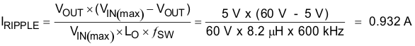
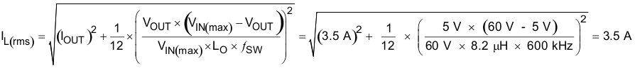
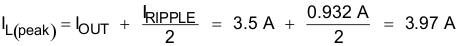
For this design example, KIND = 0.3 and the minimum inductor value is calculated to be 7.3 μH. The nearest standard value is 8.2 μH. It is important that the RMS current and saturation current ratings of the inductor not be exceeded. The RMS and peak inductor current can be found from Equation 28 and Equation 29. For this design, the RMS inductor current is 3.5 A and the peak inductor current is 3.97 A. The chosen inductor is a WE 7447797820, which has a saturation current rating of 5.8 A and an RMS current rating of 5.05 A.
As the equation set demonstrates, lower ripple currents reduce the output voltage ripple of the regulator but require a larger value of inductance. Selecting higher ripple currents increases the output voltage ripple of the regulator but allow for a lower inductance value.
The current flowing through the inductor is the inductor ripple current plus the output current. During power up, faults or transient load conditions, the inductor current can increase above the peak inductor current level calculated above. In transient conditions, the inductor current can increase up to the switch current limit of the device. For this reason, the most conservative design approach is to choose an inductor with a saturation current rating equal to or greater than the switch current limit of the TPS54360-Q1 which is nominally 5.5 A.

8.2.1.2.3 Output Capacitor
There are three primary considerations for selecting the value of the output capacitor. The output capacitor determines the modulator pole, the output voltage ripple, and how the regulator responds to a large change in load current. The output capacitance must be selected based on the most stringent of these three criteria.
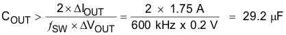
The desired response to a large change in the load current is the first criteria. The output capacitor must supply the increased load current until the regulator responds to the load step. The regulator does not respond immediately to a large, fast increase in the load current such as transitioning from no load to a full load. The regulator usually requires two or more clock cycles for the control loop to sense the change in output voltage and adjust the peak switch current in response to the higher load. The output capacitance must be large enough to supply the difference in current for 2 clock cycles to maintain the output voltage within the specified range. Equation 30 shows the minimum output capacitance necessary, where ΔIOUT is the change in output current, ƒSW is the regulators switching frequency and ΔVOUT is the allowable change in the output voltage. For this example, the transient load response is specified as a 4% change in VOUT for a load step from 0.875 A to 2.625 A. Therefore, ΔIOUT is 2.625 A - 0.875 A = 1.75 A and ΔVOUT = 0.04 × 5 = 0.2 V. Using these numbers gives a minimum capacitance of 29.2 μF. This value does not take the ESR of the output capacitor into account in the output voltage change. For ceramic capacitors, the ESR is usually small enough to be ignored. Aluminum electrolytic and tantalum capacitors have higher ESR that must be included in load step calculations.
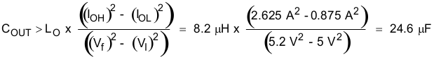
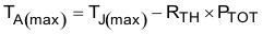
The output capacitor must also be sized to absorb energy stored in the inductor when transitioning from a high to low load current. The catch diode of the regulator can not sink current so energy stored in the inductor can produce an output voltage overshoot when the load current rapidly decreases. A typical load step response is shown in Figure 35. The excess energy absorbed in the output capacitor increases the voltage on the capacitor. The capacitor must be sized to maintain the desired output voltage during these transient periods. Equation 31 calculates the minimum capacitance required to keep the output voltage overshoot to a desired value, where LO is the value of the inductor, IOH is the output current under heavy load, IOL is the output under light load, Vf is the peak output voltage, and Vi is the initial voltage. For this example, the worst case load step is from 2.625 A to 0.875 A. The output voltage increases during this load transition and the stated maximum in our specification is 4 % of the output voltage. This makes Vf = 1.04 × 5 = 5.2. Vi is the initial capacitor voltage which is the nominal output voltage of 5 V. Using these numbers in Equation 31 yields a minimum capacitance of
24.6 μF.
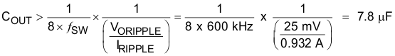
Equation 32 calculates the minimum output capacitance required to meet the output voltage ripple specification, where ƒSW is the switching frequency, VORIPPLE is the maximum allowable output voltage ripple, and IRIPPLE is the inductor ripple current. Equation 32 yields 7.8 μF.
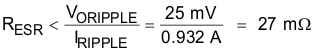
Equation 33 calculates the maximum ESR an output capacitor can have to meet the output voltage ripple specification. Equation 33 indicates the ESR must be less than 27 mΩ.
The most stringent criteria for the output capacitor is 29.2 μF required to maintain the output voltage within regulation tolerance during a load transient.
Capacitance de-ratings for aging, temperature and DC bias increases this minimum value. For this example, two 47-μF 10-V ceramic capacitors with 5 mΩ of ESR are used. The derated capacitance is 58.3 µF, well above the minimum required capacitance of 29.2 µF.
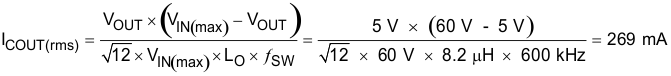
Capacitors are generally rated for a maximum ripple current that can be filtered without degrading capacitor reliability. Some capacitor data sheets specify the Root Mean Square (RMS) value of the maximum ripple current. Equation 34 can be used to calculate the RMS ripple current that the output capacitor must support. For this example, Equation 34 yields 269 mA.
8.2.1.2.4 Catch Diode
The TPS54360-Q1 requires an external catch diode between the SW pin and GND. The selected diode must have a reverse voltage rating equal to or greater than VIN(max). The peak current rating of the diode must be greater than the maximum inductor current. Schottky diodes are typically a good choice for the catch diode due to their low forward voltage. The lower the forward voltage of the diode, the higher the efficiency of the regulator.
Typically, diodes with higher voltage and current ratings have higher forward voltages. A diode with a minimum of 60 V reverse voltage is preferred to allow input voltage transients up to the rated voltage of the TPS54360-Q1.
For the example design, the B560C-13-F Schottky diode is selected for its lower forward voltage and good thermal characteristics compared to smaller devices. The typical forward voltage of the B560C-13-F is 0.70 V at 5 A.
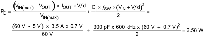
The diode must also be selected with an appropriate power rating. The diode conducts the output current during the off-time of the internal power switch. The off-time of the internal switch is a function of the maximum input voltage, the output voltage, and the switching frequency. The output current during the off-time is multiplied by the forward voltage of the diode to calculate the instantaneous conduction losses of the diode. At higher switching frequencies, the AC losses of the diode must be taken into account. The AC losses of the diode are due to the charging and discharging of the junction capacitance and reverse recovery charge. Equation 35 is used to calculate the total power dissipation, including conduction losses and AC losses of the diode.
The B560C-13-F diode has a junction capacitance of 300 pF. Using Equation 35, the worst case total loss in the diode using the maximum input voltage is 2.58 Watts.
If the power supply spends a significant amount of time at light load currents or in sleep mode, consider using a diode which has a low leakage current and slightly higher forward voltage drop.
8.2.1.2.5 Input Capacitor
The TPS54360-Q1 requires a high quality ceramic type X5R or X7R input decoupling capacitor with at least 3 μF of effective capacitance. Some applications benefit from additional bulk capacitance. The effective capacitance includes any loss of capacitance due to DC bias effects. The voltage rating of the input capacitor must be greater than the maximum input voltage. The capacitor must also have a ripple current rating greater than the maximum input current ripple of the TPS54360-Q1. The input ripple current can be calculated using Equation 36.
The value of a ceramic capacitor varies significantly with temperature and the DC bias applied to the capacitor. The capacitance variations due to temperature can be minimized by selecting a dielectric material that is more stable over temperature. X5R and X7R ceramic dielectrics are usually selected for switching regulator capacitors because they have a high capacitance to volume ratio and are fairly stable over temperature. The input capacitor must also be selected with consideration for the DC bias. The effective value of a capacitor decreases as the DC bias across a capacitor increases.
For this example design, a ceramic capacitor with at least a 60-V voltage rating is required to support the maximum input voltage. Common standard ceramic capacitor voltage ratings include 4 V, 6.3 V, 10 V, 16 V, 25 V, 50 V or 100 V. For this example, two 2.2-μF 100-V capacitors in parallel are used. Table 1 shows several choices of high voltage capacitors.
The input capacitance value determines the input ripple voltage of the regulator. The input voltage ripple can be calculated using Equation 37. Using the design example values, IOUT = 3.5 A, CIN = 4.4 μF, ƒsw = 600 kHz, yields an input voltage ripple of 331 mV and a RMS input ripple current of 1.72 A.
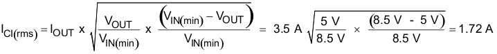
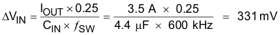
Table 1. Capacitor Types
| VENDOR | VALUE (μF) | EIA Size | VOLTAGE (V) | DIALECTRIC | COMMENTS |
|---|---|---|---|---|---|
| Murata | 1 to 2.2 | 1210 | 100 | X7R | GRM32 series |
| 1 to 4.7 | 50 | ||||
| 1 | 1206 | 100 | GRM31 series | ||
| 1 to 2.2 | 50 | ||||
| Vishay | 1 to 1.8 | 2220 | 50 | VJ X7R series | |
| 1 to 1.2 | 100 | ||||
| 1 to 3.9 | 2225 | 50 | |||
| 1 to 1.8 | 100 | ||||
| TDK | 1 to 2.2 | 1812 | 100 | C series C4532 | |
| 1.5 to 6.8 | 50 | ||||
| 1 to 2.2 | 1210 | 100 | C series C3225 | ||
| 1 to 3.3 | 50 | ||||
| AVX | 1 to 4.7 | 1210 | 50 | X7R dielectric series | |
| 1 | 100 | ||||
| 1 to 4.7 | 1812 | 50 | |||
| 1 to 2.2 | 100 |
8.2.1.2.6 Bootstrap Capacitor Selection
A 0.1-μF ceramic capacitor must be connected between the BOOT and SW pins for proper operation. A ceramic capacitor with X5R or better grade dielectric is recommended. The capacitor should have a 10 V or higher voltage rating.
8.2.1.2.7 Undervoltage Lockout Set Point
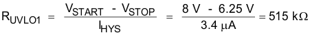
The Undervoltage Lockout (UVLO) is adjusted using an external voltage divider on the EN pin of the TPS54360-Q1. The UVLO has two thresholds, one for power up when the input voltage is rising and one for power down or brown outs when the input voltage is falling. For the example design, the supply should turn on and start switching once the input voltage increases above 8 V (UVLO start). After the regulator starts switching, it should continue to do so until the input voltage falls below 6.25 V (UVLO stop).
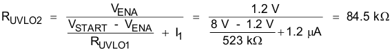
Programmable UVLO threshold voltages are set using the resistor divider of RUVLO1 and RUVLO2 between Vin and ground connected to the EN pin. Equation 2 and Equation 3 calculate the resistance values necessary. For the example application, a 523 kΩ between Vin and EN (RUVLO1) and a 84.5 kΩ between EN and ground (RUVLO2) are required to produce the 8 V and 6.25 V start and stop voltages.
8.2.1.2.8 Output Voltage and Feedback Resistors Selection
The voltage divider of R5 and R6 sets the output voltage. For the example design, 10.2 kΩ was selected for R6. Using Equation 1, R5 is calculated as 53.5 kΩ. The nearest standard 1% resistor is 53.6 kΩ. Due to the input current of the FB pin, the current flowing through the feedback network must be greater than 1 μA to maintain the output voltage accuracy. This requirement is satisfied if the value of R6 is less than 800 kΩ. Choosing higher resistor values decreases quiescent current and improves efficiency at low output currents but can also introduce noise immunity problems.

8.2.1.2.9 Compensation
There are several methods to design compensation for DC-DC regulators. The method presented here is easy to calculate and ignores the effects of the slope compensation that is internal to the device. Because the slope compensation is ignored, the actual crossover frequency is lower than the crossover frequency used in the calculations. This method assumes the crossover frequency is between the modulator pole and the ESR zero and the ESR zero is at least 10 times greater the modulator pole.
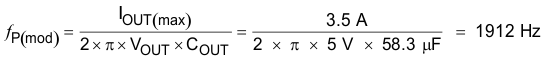
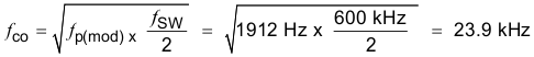
To get started, the modulator pole, ƒp(mod), and the ESR zero, ƒz1 must be calculated using Equation 41 and Equation 42. For COUT, use a derated value of 58.3 μF. Use equations Equation 43 and Equation 44 to estimate a starting point for the crossover frequency, ƒco. For the example design, ƒp(mod) is 1912 Hz and ƒz(mod) is 1092 kHz. Equation 42 is the geometric mean of the modulator pole and the ESR zero and Equation 44 is the mean of modulator pole and the switching frequency. Equation 43 yields 45.7 kHz and Equation 44 gives 23.9 kHz. Use the lower value of Equation 43 or Equation 44 for an initial crossover frequency. For this example, the target ƒco is 23.9 kHz.
Next, the compensation components are calculated. A resistor in series with a capacitor is used to create a compensating zero. A capacitor in parallel to these two components forms the compensating pole.


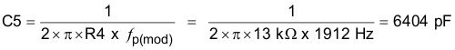
To determine the compensation resistor, R4, use Equation 45. Assume the power stage transconductance, gmps, is 12 A/V. The output voltage, VO, reference voltage, VREF, and amplifier transconductance, gmea, are 5 V, 0.8 V and 350 μA/V, respectively. R4 is calculated to be 13 kΩ which is a standard value. Use Equation 46 to set the compensation zero to the modulator pole frequency. Equation 46 yields 6404 pF for compensating capacitor C5. 6800 pF is used for this design.

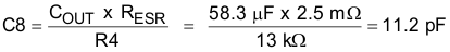
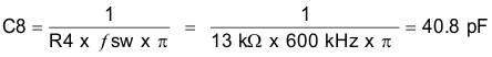
A compensation pole can be implemented if desired by adding capacitor C8 in parallel with the series combination of R4 and C5. Use the larger value calculated from Equation 47 and Equation 48 for C8 to set the compensation pole. The selected value of C8 is 39 pF for this design example.
8.2.1.2.10 Discontinuous Conduction Mode and Eco-Mode™ Boundary
With an input voltage of 12 V, the power supply enters discontinuous conduction mode when the output current is less than 300 mA. The power supply enters Eco-Mode when the output current is lower than 24 mA. The input current draw is 270 μA with no load.
8.2.1.2.11 Power Dissipation Estimate
The following formulas show how to estimate the TPS54360-Q1 power dissipation under continuous conduction mode (CCM) operation. These equations should not be used if the device is operating in discontinuous conduction mode (DCM).
The power dissipation of the IC includes conduction loss (PCOND), switching loss (PSW), gate drive loss (PGD) and supply current (PQ). Example calculations are shown with the 12 V typical input voltage of the design example.


Where:
- IOUT is the output current (A)
- RDS(on) is the on-resistance of the high-side MOSFET (Ω)
- VOUT is the output voltage (V)
- VIN is the input voltage (V)
- ƒSW is the switching frequency (Hz)
- trise is the SW-pin voltage rise time and is estimated by trise = VIN × 0.16 ns/V + 3 ns
- QG is the total gate charge of the internal MOSFET
- IQ is the operating nonswitching supply current
Therefore,

For given TA,
For given TJMAX = 150°C
Where:
- PTOT is the total device power dissipation (W)
- TA is the ambient temperature (°C)
- TJ is the junction temperature (°C)
- RTH is the thermal resistance of the package (°C/W)
- TJ(max) is maximum junction temperature (°C)
- TA(max) is maximum ambient temperature (°C)
There are additional power losses in the regulator circuit due to the inductor AC and DC losses, the catch diode and PCB trace resistance impacting the overall efficiency of the regulator.
8.2.1.3 Application Curves
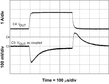 Figure 35. Load Transient
 Figure 37. Startup With VIN
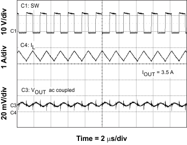 Figure 39. Output Ripple CCM
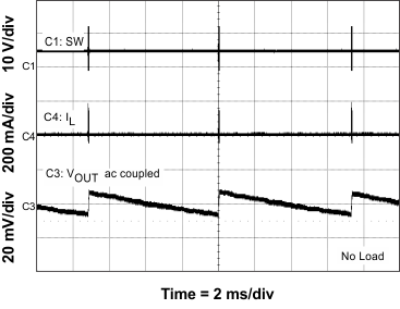 Figure 41. Output Ripple PSM
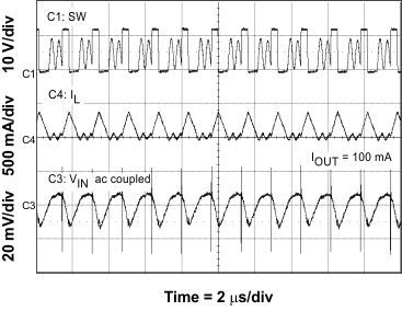 Figure 43. Input Ripple DCM
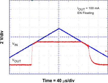 Figure 45. Low Dropout Operation
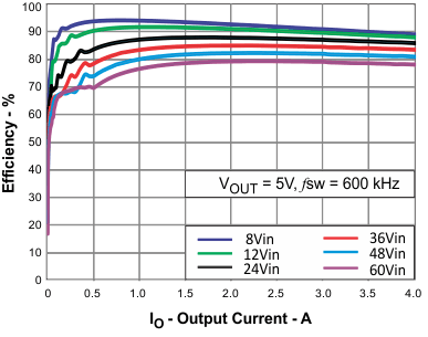 Figure 47. Efficiency vs Load Current
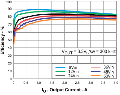 Figure 49. Efficiency vs Load Current
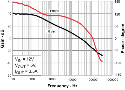 Figure 51. Overall Loop Frequency Response
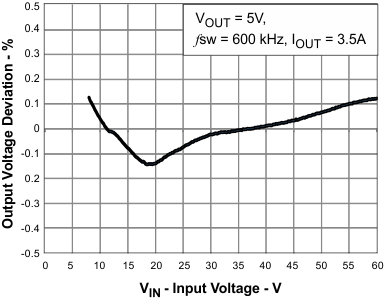 Figure 53. Regulation vs Input Voltage
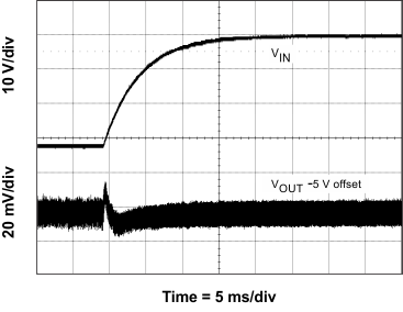 Figure 36. Line Transient (8 V To 40 V)
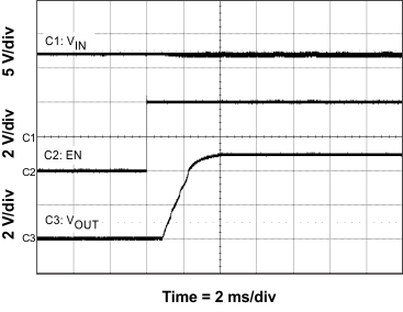 Figure 38. Startup With EN
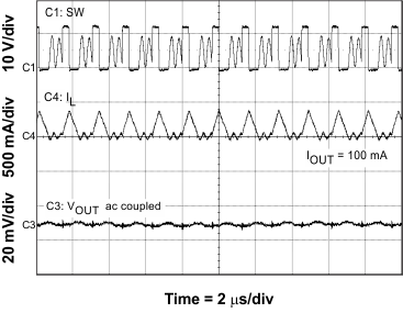 Figure 40. Output Ripple DCM
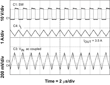 Figure 42. Input Ripple CCM
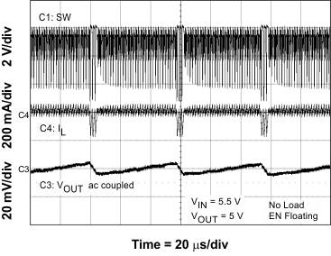 Figure 44. Low Dropout Operation
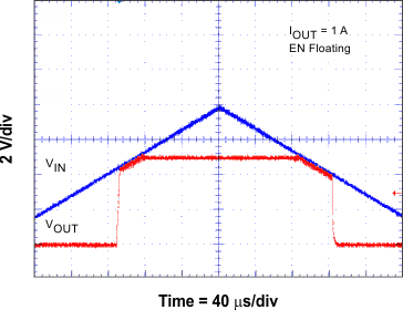 Figure 46. Low Dropout Operation
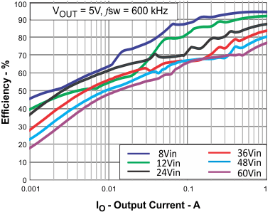 Figure 48. Light Load Efficiency
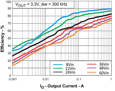 Figure 50. Light Load Efficiency
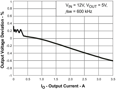 Figure 52. Regulation vs Load Current
8.2.2 TPS54360-Q1 Inverting Power Supply
The TPS54360-Q1 can be used to convert a positive input voltage to a negative output voltage. Example applications are amplifiers requiring a negative power supply.
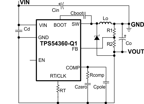 Figure 54. TPS54360-Q1 Inverting Power Supply
8.2.3 TPS54360-Q1 Split Rail Power Supply
The TPS54360-Q1 device can be used to convert a positive input voltage to a split rail positive and negative output voltage by using a coupled inductor. Example applications are amplifiers requiring a split rail positive and negative voltage power supply.
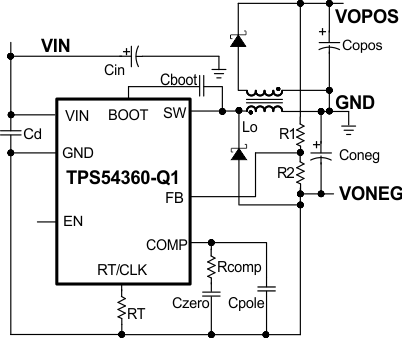 Figure 55. TPS54360-Q1 Split Rail Power Supply