SLVSBZ2A September 2013 – November 2014 TPS54360-Q1
PRODUCTION DATA.
- 1 Features
- 2 Applications
- 3 Description
- 4 Revision History
- 5 Pin Configuration and Functions
- 6 Specifications
-
7 Detailed Description
- 7.1 Overview
- 7.2 Functional Block Diagram
- 7.3
Feature Description
- 7.3.1 Fixed Frequency PWM Control
- 7.3.2 Slope Compensation Output Current
- 7.3.3 Pulse Skip Eco-Mode™
- 7.3.4 Low Dropout Operation and Bootstrap Voltage (BOOT)
- 7.3.5 Error Amplifier
- 7.3.6 Adjusting the Output Voltage
- 7.3.7 Enable and Adjusting Undervoltage Lockout
- 7.3.8 Internal Soft-Start
- 7.3.9 Constant Switching Frequency and Timing Resistor (RT/CLK) Pin)
- 7.3.10 Accurate Current Limit Operation and Maximum Switching Frequency
- 7.3.11 Synchronization to RT/CLK Pin
- 7.3.12 Overvoltage Protection
- 7.3.13 Thermal Shutdown
- 7.3.14 Small Signal Model for Loop Response
- 7.3.15 Simple Small Signal Model for Peak Current Mode Control
- 7.3.16 Small Signal Model for Frequency Compensation
- 7.4 Device Functional Modes
-
8 Application and Implementation
- 8.1 Application Information
- 8.2
Typical Application
- 8.2.1
5-V Output TPS54360-Q1 Design Example
- 8.2.1.1 Design Requirements
- 8.2.1.2
Detailed Design Procedure
- 8.2.1.2.1 Selecting the Switching Frequency
- 8.2.1.2.2 Output Inductor Selection (LO)
- 8.2.1.2.3 Output Capacitor
- 8.2.1.2.4 Catch Diode
- 8.2.1.2.5 Input Capacitor
- 8.2.1.2.6 Bootstrap Capacitor Selection
- 8.2.1.2.7 Undervoltage Lockout Set Point
- 8.2.1.2.8 Output Voltage and Feedback Resistors Selection
- 8.2.1.2.9 Compensation
- 8.2.1.2.10 Discontinuous Conduction Mode and Eco-Mode™ Boundary
- 8.2.1.2.11 Power Dissipation Estimate
- 8.2.1.3 Application Curves
- 8.2.2 TPS54360-Q1 Inverting Power Supply
- 8.2.3 TPS54360-Q1 Split Rail Power Supply
- 8.2.1
5-V Output TPS54360-Q1 Design Example
- 9 Power Supply Recommendations
- 10Layout
- 11Device and Documentation Support
- 12Mechanical, Packaging, and Orderable Information
パッケージ・オプション
メカニカル・データ(パッケージ|ピン)
- DDA|8
サーマルパッド・メカニカル・データ
- DDA|8
発注情報
7 Detailed Description
7.1 Overview
The TPS54360-Q1 is a 60-V, 3.5-A, step-down (buck) regulator with an integrated high-side n-channel MOSFET. The device implements constant frequency, current mode control which reduces output capacitance and simplifies external frequency compensation. The wide switching frequency range of 100 kHz to 2500 kHz allows either efficiency or size optimization when selecting the output filter components. The switching frequency is adjusted using a resistor to ground connected to the RT/CLK pin. The device has an internal phase-locked loop (PLL) connected to the RT/CLK pin that synchronizes the power switch turn on to a falling edge of an external clock signal.
The TPS54360-Q1 has a default input start-up voltage of approximately 4.3 V. The EN pin can be used to adjust the input voltage undervoltage lockout (UVLO) threshold with two external resistors. An internal pull up current source enables operation when the EN pin is floating. The operating current is 146 μA under no load condition (not switching). When the device is disabled, the supply current is 2 μA.
The integrated 92-mΩ high-side MOSFET supports high efficiency power supply designs capable of delivering 3.5 A of continuous current to a load. The gate drive bias voltage for the integrated high-side MOSFET is supplied by a bootstrap capacitor connected from the BOOT to SW pins. The TPS54360-Q1 reduces the external component count by integrating the bootstrap recharge diode. The BOOT pin capacitor voltage is monitored by a UVLO circuit which turns off the high-side MOSFET when the BOOT to SW voltage falls below a preset threshold. An automatic BOOT capacitor recharge circuit allows the TPS54360-Q1 to operate at high duty cycles approaching 100%. Therefore, the maximum output voltage is near the minimum input supply voltage of the application. The minimum output voltage is the internal 0.8 V feedback reference.
Output overvoltage transients are minimized by an Overvoltage Transient Protection (OVP) comparator. When the OVP comparator is activated, the high-side MOSFET is turned off and remains off until the output voltage is less than 106% of the desired output voltage.
The TPS54360-Q1 includes an internal soft-start circuit that slows the output rise time during start-up to reduce in-rush current and output voltage overshoot. Output overload conditions reset the soft-start timer. When the overload condition is removed, the soft-start circuit controls the recovery from the fault output level to the nominal regulation voltage. A frequency foldback circuit reduces the switching frequency during start-up and overcurrent fault conditions to help maintain control of the inductor current.
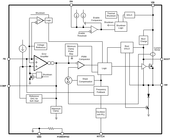
7.2 Functional Block Diagram
7.3 Feature Description
7.3.1 Fixed Frequency PWM Control
The TPS54360-Q1 uses fixed frequency, peak current mode control with adjustable switching frequency. The output voltage is compared through external resistors connected to the FB pin to an internal voltage reference by an error amplifier. An internal oscillator initiates the turn on of the high-side power switch. The error amplifier output at the COMP pin controls the high-side power switch current. When the high-side MOSFET switch current reaches the threshold level set by the COMP voltage, the power switch is turned off. The COMP-pin voltage increases and decreases as the output current increases and decreases. The device implements current limiting by clamping the COMP-pin voltage to a maximum level. The pulse skipping Eco-Mode is implemented with a minimum voltage clamp on the COMP pin.
7.3.2 Slope Compensation Output Current
The TPS54360-Q1 adds a compensating ramp to the MOSFET switch current sense signal. This slope compensation prevents sub-harmonic oscillations at duty cycles greater than 50%. The peak current limit of the high-side switch is not affected by the slope compensation and remains constant over the full duty cycle range.
7.3.3 Pulse Skip Eco-Mode™
The TPS54360-Q1 operates in a pulse skipping Eco-mode at light load currents to improve efficiency by reducing switching and gate drive losses. If the output voltage is within regulation and the peak switch current at the end of any switching cycle is below the pulse skipping current threshold, the device enters Eco-Mode. The pulse skipping current threshold is the peak switch current level corresponding to a nominal COMP voltage of 600 mV.
When in Eco-Mode, the COMP-pin voltage is clamped at 600 mV and the high-side MOSFET is inhibited. Because the device is not switching, the output voltage begins to decay. The voltage control loop responds to the falling output voltage by increasing the COMP-pin voltage. The high-side MOSFET is enabled and switching resumes when the error amplifier lifts COMP above the pulse skipping threshold. The output voltage recovers to the regulated value, and COMP eventually falls below the Eco-Mode pulse skipping threshold at which time the device again enters Eco-Mode. The internal PLL remains operational when in Eco-Mode. When operating at light load currents in Eco-Mode, the switching transitions occur synchronously with the external clock signal.
During Eco-Mode operation, the TPS54360-Q1 senses and controls peak switch current, not the average load current. Therefore the load current at which the device enters Eco-Mode is dependent on the output inductor value. The circuit in Figure 34 enters Eco-Mode at about 24 mA output current. As the load current approaches zero, the device enters a pulse skip mode during which it draws only 146 μA input quiescent current.
7.3.4 Low Dropout Operation and Bootstrap Voltage (BOOT)
The TPS54360-Q1 provides an integrated bootstrap voltage regulator. A small capacitor between the BOOT and SW pins provides the gate drive voltage for the high-side MOSFET. The BOOT capacitor is refreshed when the high-side MOSFET is off and the external low-side diode conducts. The recommended value of the BOOT capacitor is 0.1 μF. A ceramic capacitor with an X7R or X5R grade dielectric with a voltage rating of 10 V or higher is recommended for stable performance over temperature and voltage.
When operating with a low voltage difference from input to output, the high-side MOSFET of the TPS54360-Q1 operates at 100% duty cycle as long as the BOOT to SW-pin voltage is greater than 2.1 V. When the voltage from BOOT to SW drops below 2.1V, the high-side MOSFET is turned off and an integrated low-side MOSFET pulls SW low to recharge the BOOT capacitor. To reduce the losses of the small low-side MOSFET at high output voltages, it is disabled at 24 V output and re-enabled when the output reaches 21.5 V.
Because the gate drive current sourced from the BOOT capacitor is small, the high-side MOSFET can remain on for many switching cycles before the MOSFET is turned off to refresh the capacitor. Thus the effective duty cycle of the switching regulator can be high, approaching 100%. The effective duty cycle of the converter during dropout is mainly influenced by the voltage drops across the power MOSFET, the inductor resistance, the low-side diode voltage and the printed circuit board resistance.
The start and stop voltage for a typical 5 V output application is shown in Figure 22 where the Vin voltage is plotted versus load current. The start voltage is defined as the input voltage required to regulate the output within 1% of nominal. The stop voltage is defined as the input voltage at which the output drops by 5% or where switching stops.
During high duty cycle (low dropout) conditions, inductor current ripple increases when the BOOT capacitor is being recharged resulting in an increase in output voltage ripple. Increased ripple occurs when the off time required to recharge the BOOT capacitor is longer than the high-side off time associated with cycle by cycle PWM control.
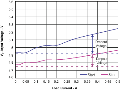 Figure 22. 5 V Start / Stop Voltage
7.3.5 Error Amplifier
The TPS54360-Q1 voltage regulation loop is controlled by a transconductance error amplifier. The error amplifier compares the FB-pin voltage to the lower of the internal soft-start voltage or the internal 0.8 V voltage reference. The transconductance (gm) of the error amplifier is 350 μS during normal operation. During soft-start operation, the transconductance is reduced to 78 μS and the error amplifier is referenced to the internal soft-start voltage.
The frequency compensation components (capacitor, series resistor and capacitor) are connected between the error amplifier output COMP pin and GND pin.
7.3.6 Adjusting the Output Voltage
The internal voltage reference produces a precise 0.8 V ±1% voltage reference over the operating temperature and voltage range by scaling the output of a bandgap reference circuit. The output voltage is set by a resistor divider from the output node to the FB pin. TI recommends to use 1% tolerance or better divider resistors. Select the low-side resistor RLS for the desired divider current and use Equation 1 to calculate RHS. To improve efficiency at light loads consider using larger value resistors. However, if the values are too high, the regulator is more susceptible to noise and voltage errors from the FB input current can become noticeable.

7.3.7 Enable and Adjusting Undervoltage Lockout
The TPS54360-Q1 is enabled when the VIN-pin voltage rises above 4.3 V and the EN-pin voltage exceeds the enable threshold of 1.2 V. The TPS54360-Q1 is disabled when the VIN-pin voltage falls below 4 V or when the EN-pin voltage is below 1.2 V. The EN pin has an internal pullup current source, I1, of 1.2 μA that enables operation of the TPS54360-Q1 when the EN pin floats.
If an application requires a higher undervoltage lockout (UVLO) threshold, use the circuit shown in Figure 23 to adjust the input voltage UVLO with two external resistors. When the EN-pin voltage exceeds 1.2 V, an additional 3.4 μA of hysteresis current, Ihys, is sourced out of the EN pin. When the EN pin is pulled below 1.2 V, the 3.4 μA Ihys current is removed. This addional current facilitates adjustable input voltage UVLO hysteresis. Use Equation 2 to calculate RUVLO1 for the desired UVLO hysteresis voltage. Use Equation 3 to calculate RUVLO2 for the desired VIN start voltage.
In applications designed to start at relatively low input voltages (such as, from 4.5 V to 9 V) and withstand high input voltages (such as, from 40 V to 60 V), the EN pin experiences a voltage greater than the absolute maximum voltage of 8.4 V during the high input voltage condition. When using an external EN resistor divider the EN pin voltage is clamped internally with a 5.8 V zener diode. The zener diode will sink up to 150 µA.
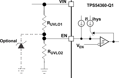 Figure 23. Adjustable Undervoltage Lockout (UVLO)
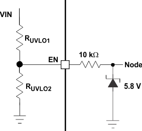 Figure 24. Internal EN Clamp


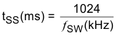
7.3.8 Internal Soft-Start
The TPS54360-Q1 has an internal digital soft-start that ramps the reference voltage from 0 V to the final value in 1024 switching cycles. The internal soft-start time (10% to 90%) is calculated using Equation 4
If the EN pin is pulled below the stop threshold of 1.2 V, switching stops and the internal soft-start resets. The soft-start also resets in thermal shutdown.
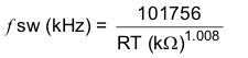
7.3.9 Constant Switching Frequency and Timing Resistor (RT/CLK) Pin)
The switching frequency of the TPS54360-Q1 is adjustable over a wide range from 100 kHz to 2500 kHz by placing a resistor between the RT/CLK pin and GND pin. The RT/CLK-pin voltage is typically 0.5 V and must have a resistor to ground to set the switching frequency. To determine the timing resistance for a given switching frequency, use Equation 5 or Equation 6 or the curves in Figure 5 and Figure 6. To reduce the solution size one would typically set the switching frequency as high as possible, but tradeoffs of the conversion efficiency, maximum input voltage and minimum controllable on time must be considered. The minimum controllable on time is typically 135 ns which limits the maximum operating frequency in applications with high input to output step down ratios. The maximum switching frequency is also limited by the frequency foldback circuit. A more detailed discussion of the maximum switching frequency is provided in the next section.

7.3.10 Accurate Current Limit Operation and Maximum Switching Frequency
The TPS54360-Q1 implements peak current mode control in which the COMP-pin voltage controls the peak current of the high-side MOSFET. A signal proportional to the high-side switch current and the COMP-pin voltage are compared each cycle. When the peak switch current intersects the COMP control voltage, the high-side switch is turned off. During overcurrent conditions that pull the output voltage low, the error amplifier increases switch current by driving the COMP pin high. The error amplifier output is clamped internally at a level which sets the peak switch current limit. The TPS54360-Q1 provides an accurate current limit threshold with a typical current limit delay of 60 ns. With smaller inductor values, the delay results in a higher peak inductor current. The relationship between the inductor value and the peak inductor current is shown in Figure 25.
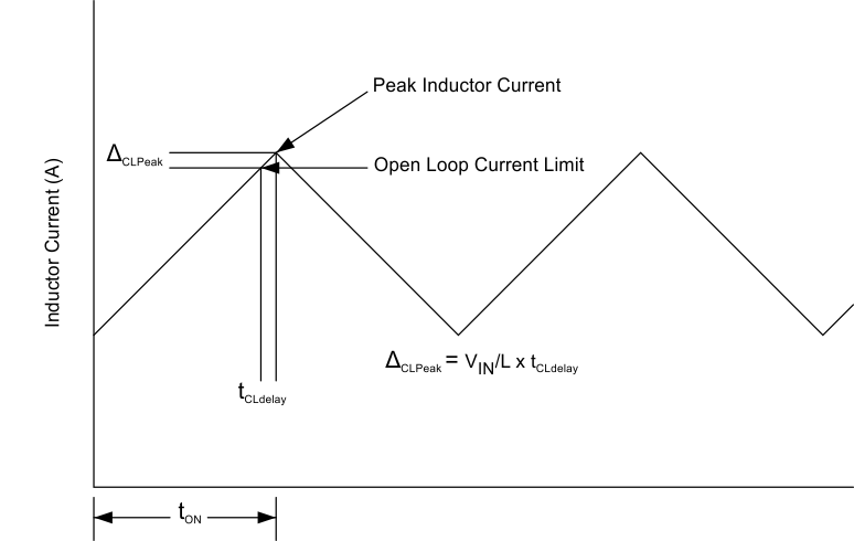 Figure 25. Current Limit Delay
To protect the converter in overload conditions at higher switching frequencies and input voltages, the TPS54360-Q1 implements a frequency foldback. The oscillator frequency is divided by 1, 2, 4, and 8 as the FB-pin voltage falls from 0.8 V to 0 V. The TPS54360-Q1 uses a digital frequency foldback to enable synchronization to an external clock during normal start-up and fault conditions. During short-circuit events, the inductor current can exceed the peak current limit because of the high input voltage and the minimum controllable on time. When the output voltage is forced low by the shorted load, the inductor current decreases slowly during the switch-off time. The frequency foldback effectively increases the off time by increasing the period of the switching cycle providing more time for the inductor current to ramp down.
With a maximum frequency foldback ratio of 8, there is a maximum frequency at which the inductor current is controlled by frequency foldback protection. Equation 8 calculates the maximum switching frequency at which the inductor current remains under control when VOUT is forced to VOUT(SC). The selected operating frequency must not exceed the calculated value.
Equation 7 calculates the maximum switching frequency limitation set by the minimum controllable on time and the input to output step down ratio. Setting the switching frequency above this value causes the regulator to skip switching pulses to achieve the low duty cycle required at maximum input voltage.

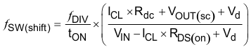
| IO | Output current |
| ICL | Current limit |
| Rdc | inductor resistance |
| VIN | maximum input voltage |
| VOUT | output voltage |
| VOUTSC | output voltage during short |
| Vd | diode voltage drop |
| RDS(on) | switch on resistance |
| tON | minimum controllable on time |
| ƒDIV | frequency divide equals (1, 2, 4, or 8) |
7.3.11 Synchronization to RT/CLK Pin
The RT/CLK pin can receive a frequency synchronization signal from an external system clock. To implement this synchronization feature connect a square wave to the RT/CLK pin through either circuit network shown in Figure 26. The square wave applied to the RT/CLK pin must switch lower than 0.5 V and higher than 1.7 V and have a pulse-width greater than 15 ns. The synchronization frequency range is 160 kHz to 2300 kHz. The rising edge of the SW synchronizes to the falling edge of RT/CLK pin signal. The external synchronization circuit must be designed such that the default frequency set resistor is connected from the RT/CLK pin to ground when the synchronization signal is off. When using a low impedance signal source, the frequency set resistor is connected in parallel with an AC-coupling capacitor to a termination resistor (for example: 50 Ω) as shown in Figure 26. The two resistors in series provide the default frequency setting resistance when the signal source is turned off. The sum of the resistance should set the switching frequency close to the external CLK frequency. TI recommends to AC couple the synchronization signal through a 10 pF ceramic capacitor to RT/CLK pin.
The first time the RT/CLK is pulled above the PLL threshold the TPS54360-Q1 switches from the RT resistor free-running frequency mode to the PLL synchronized mode. The internal 0.5 V voltage source is removed and the RT/CLK pin becomes high impedance as the PLL starts to lock onto the external signal. The switching frequency can be higher or lower than the frequency set with the RT/CLK resistor. The device transitions from the resistor mode to the PLL mode and locks onto the external clock frequency within 78 µs. During the transition from the PLL mode to the resistor programmed mode, the switching frequency falls to 150 kHz and then increases or decreases to the resistor programmed frequency when the 0.5-V bias voltage is reapplied to the RT/CLK resistor.
The switching frequency is divided by 8, 4, 2, and 1 as the FB-pin voltage ramps from 0 to 0.8 V. The device implements a digital frequency foldback to enable synchronizing to an external clock during normal start-up and fault conditions. Figure 27, Figure 28 and Figure 29 show the device synchronized to an external system clock in continuous conduction mode (CCM), discontinuous conduction (DCM), and pulse skip mode (Eco-Mode).
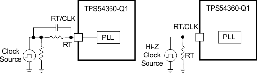 Figure 26. Synchronizing to a System Clock
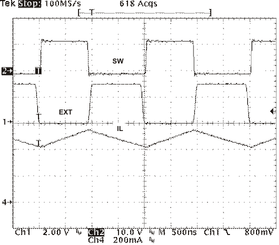 Figure 27. Plot of Synchronizing in CCM
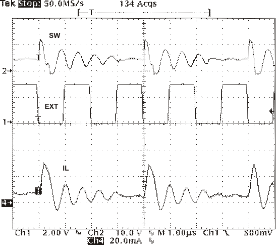 Figure 29. Plot of Synchronizing in Eco-Mode™
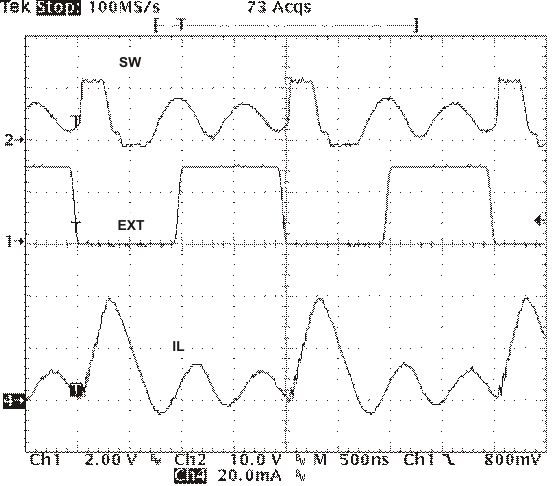 Figure 28. Plot of Synchronizing in DCM
7.3.12 Overvoltage Protection
The TPS54360-Q1 incorporates an output overvoltage protection (OVP) circuit to minimize voltage overshoot when recovering from output fault conditions or strong unload transients in designs with low output capacitance. For example, when the power supply output is overloaded the error amplifier compares the actual output voltage to the internal reference voltage. If the FB-pin voltage is lower than the internal reference voltage for a considerable time, the output of the error amplifier increases to a maximum voltage corresponding to the peak current limit threshold. When the overload condition is removed, the regulator output rises and the error amplifier output transitions to the normal operating level. In some applications, the power supply output voltage increases faster than the response of the error amplifier output resulting in an output overshoot.
The OVP feature minimizes output overshoot when using a low value output capacitor by comparing the FB-pin voltage to the rising OVP threshold which is nominally 109% of the internal voltage reference. If the FB-pin voltage is greater than the rising OVP threshold, the high-side MOSFET is immediately disabled to minimize output overshoot. When the FB voltage drops below the falling OVP threshold which is nominally 106% of the internal voltage reference, the high-side MOSFET resumes normal operation.
7.3.13 Thermal Shutdown
The TPS54360-Q1 provides an internal thermal shutdown to protect the device when the junction temperature exceeds 176°C. The high-side MOSFET stops switching when the junction temperature exceeds the thermal trip threshold. Once the die temperature falls below 164°C, the device reinitiates the power up sequence controlled by the internal soft-start circuitry.
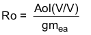
7.3.14 Small Signal Model for Loop Response
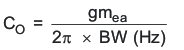
Figure 30 shows an equivalent model for the TPS54360-Q1 control loop which can be simulated to check the frequency response and dynamic load response. The error amplifier is a transconductance amplifier with a gmEA of 350 μS. The error amplifier can be modeled using an ideal voltage controlled current source. The resistor Ro and capacitor Co model, the open-loop gain, and frequency response of the amplifier. The 1-mV AC voltage source between the nodes a and b effectively breaks the control loop for the frequency response measurements. Plotting c/a provides the small signal response of the frequency compensation. Plotting a/b provides the small signal response of the overall loop. The dynamic loop response can be evaluated by replacing RL with a current source with the appropriate load step amplitude and step rate in a time domain analysis. This equivalent model is only valid for continuous conduction mode (CCM) operation.
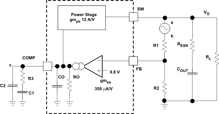 Figure 30. Small Signal Model For Loop Response
7.3.15 Simple Small Signal Model for Peak Current Mode Control
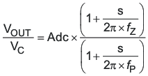
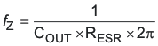
Figure 31 describes a simple small signal model that can be used to design the frequency compensation. The TPS54360-Q1 power stage can be approximated by a voltage-controlled current source (duty cycle modulator) supplying current to the output capacitor and load resistor. The control to output transfer function is shown in Equation 9 and consists of a DC gain, one dominant pole, and one ESR zero. The quotient of the change in switch current and the change in COMP-pin voltage (node c in Figure 30) is the power stage transconductance, gmPS. The gmPS for the TPS54360-Q1 is 12 A/V. The low-frequency gain of the power stage is the product of the transconductance and the load resistance as shown in Equation 10.
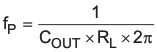
As the load current increases and decreases, the low-frequency gain decreases and increases, respectively. This variation with the load is problematic at first glance, but fortunately the dominant pole moves with the load current (see Equation 11). The combined effect is highlighted by the dashed line in the right half of Figure 31. As the load current decreases, the gain increases and the pole frequency lowers, keeping the 0-dB crossover frequency the same with varying load conditions. The type of output capacitor chosen determines whether the ESR zero has a profound effect on the frequency compensation design. Using high-ESR aluminum-electrolytic capacitors can reduce the number frequency compensation components required to stabilize the overall loop because the phase margin is increased by the ESR zero of the output capacitor (see Equation 12).
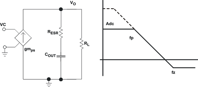 Figure 31. Simple Small Signal Model and Frequency Response for Peak Current Mode Control

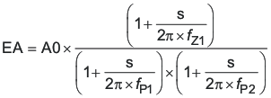
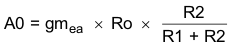
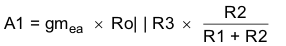
7.3.16 Small Signal Model for Frequency Compensation
The TPS54360-Q1 uses a transconductance amplifier for the error amplifier and supports three of the commonly-used frequency compensation circuits. Compensation circuits Type 2A, Type 2B, and Type 1 are shown in Figure 32. Type 2 circuits are typically implemented in high bandwidth power-supply designs using low-ESR output capacitors. The Type 1 circuit is used with power-supply designs with high-ESR aluminum-electrolytic or tantalum capacitors. Equation 13 and Equation 14 relate the frequency response of the amplifier to the small signal model in Figure 32. The open-loop gain and bandwidth are modeled using the RO and CO shown in Figure 32. See the application section for a design example using a Type 2A network with a low ESR output capacitor.
Equation 13 through Equation 22 are provided as a reference. An alternative is to use WEBENCH software tools to create a design based on the power supply requirements.
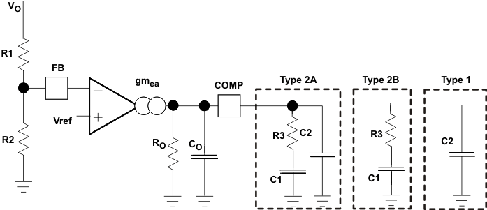 Figure 32. Types of Frequency Compensation
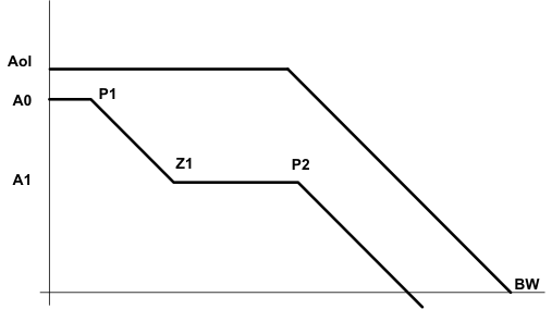 Figure 33. Frequency Response of the Type 2A and Type 2B Frequency Compensation


7.4 Device Functional Modes
7.4.1 Operation near Minimum VIN (VVIN = < 4.5 V)
The TPS54360-Q1 is designed to operate with input voltage above 4.5 V. The typical VIN UVLO threshold is 4.3 V and the device may operate at input voltages down to the UVLO voltage. At input voltages below the UVLO voltage the device does not switch. If an external resistor divider pulls the EN pin up to VIN or the EN pin is floating, when VIN passes the UVLO threshold the device becomes active. When the device is active switching begins and the soft-start sequence initiates. The TPS54360-Q1 ramps up the output voltage at a rate based on the internal digital soft-start.
7.4.2 Operation with EN Control
The enabled threshold voltage is 1.2 V typical. With EN held below the threshold voltage the device is shut down and switching is inhibited even if the VIN voltage is above its UVLO threshold. The IC quiescent current decreases to a minimum in this state. If the EN pin voltage is increased above its threshold while the VIN voltage is also above its UVLO threshold, the device becomes active. When the device is active switching begins and the soft-start sequence initiates. The TPS54360-Q1 ramps up the output voltage at a rate based on the internal digital soft-start