SLVSA31A November 2009 – December 2014 TPS61029-Q1
PRODUCTION DATA.
- 1 Features
- 2 Applications
- 3 Description
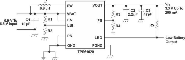
- 4 Simplified Schematic
- 5 Revision History
- 6 Device Comparison Table
- 7 Pin Configuration and Functions
- 8 Specifications
- 9 Typical Characteristics
- 10Parameter Measurement Information
- 11Detailed Description
- 12Application and Implementation
- 13Power Supply Recommendations
- 14Layout
- 15Device and Documentation Support
- 16Mechanical, Packaging, and Orderable Information
パッケージ・オプション
デバイスごとのパッケージ図は、PDF版データシートをご参照ください。
メカニカル・データ(パッケージ|ピン)
- DPN|10
- DRC|10
サーマルパッド・メカニカル・データ
- DRC|10
発注情報
1 Features
- Qualified for Automotive Applications
- 96% Efficient Synchronous Boost Converter
- Output Voltage Remains Regulated When Input Voltage Exceeds Nominal Output Voltage
- Device Quiescent Current: 25 µA (Typ)
- Input Voltage Range: 0.9 V to 6.5 V
- Fixed and Adjustable Output Voltage Options Up to 5.5 V
- Power Save Mode for Improved Efficiency at Low Output Power
- Low Battery Comparator
- Low EMI-Converter (Integrated Anti-ringing Switch)
- Load Disconnect During Shutdown
- Over-Temperature Protection
- Small 3-mm × 3-mm QFN-10 Package
2 Applications
- All One-Cell, Two-Cell and Three-Cell Alkaline, NiCd or NiMH or Single-Cell Li Battery Powered Products
- Portable Audio Players
- PDAs
- Cellular Phones
- Personal Medical Products
- Camera White LED Flash Light
3 Description
The TPS6102x devices provide a power supply solution for products powered by either a one-cell, two-cell, or three-cell alkaline, NiCd or NiMH, or one-cell Li-Ion or Li-polymer battery. Output currents can go as high as 200 mA while using a single-cell alkaline, and discharge it down to 0.9 V. It can also be used for generating 5 V at 500 mA from a 3.3-V rail or a Li-Ion battery. The boost converter is based on a fixed frequency, pulse-width-modulation (PWM) controller using a synchronous rectifier to obtain maximum efficiency. At low load currents, the converter enters the Power Save Mode to maintain a high efficiency over a wide load current range. The Power Save Mode can be disabled, forcing the converter to operate at a fixed switching frequency. The maximum peak current in the boost switch is limited to a value of 800 mA, 1500 mA or 1800 mA depending on the device version.
The TPS6102x devices keep the output voltage regulated even when the input voltage exceeds the nominal output voltage. The output voltage can be programmed by an external resistor divider, or is fixed internally on the chip. The converter can be disabled to minimize battery drain. During shutdown, the load is completely disconnected from the battery. A low-EMI mode is implemented to reduce ringing and, in effect, lower radiated electromagnetic energy when the converter enters the discontinuous conduction mode. The device is packaged in a 10-pin VSON PowerPAD™ package.
Device Information(1)
| PART NUMBER | PACKAGE | BODY SIZE (NOM) |
|---|---|---|
| TPS61025-Q1 | VSON (10) | 3.00mm x 3.00mm |
| TPS61027-Q1 | ||
| TPS61029-Q1 |
- For all available packages, see the orderable addendum at the end of the datasheet.
4 Simplified Schematic