SLVS789D November 2007 – December 2014 TPS61170
PRODUCTION DATA.
- 1 Features
- 2 Applications
- 3 Description
- 4 Typical Application Schematic
- 5 Revision History
- 6 Pin Configuration and Functions
- 7 Specifications
- 8 Detailed Description
- 9 Application and Implementation
- 10Power Supply Recommendations
- 11Layout
- 12Device and Documentation Support
- 13Mechanical, Packaging, and Orderable Information
6 Pin Configuration and Functions
QFN Package
6 Pins
Top View
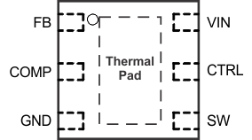
Pin Functions
| PIN | I/O | DESCRIPTION | |
|---|---|---|---|
| NAME | NO. | ||
| COMP | 2 | O | Output of the transconductance error amplifier. Connect an external RC network to this pin to compensate the regulator. |
| CTRL | 5 | I | Control pin of the boost regulator. CTRL is a multifunctional pin which can be used to enable the device and control the feedback voltage with a PWM signal or for digital communications. |
| FB | 1 | I | Feedback pin for current. Connect to the center tap of a resistor divider to program the output voltage. |
| GND | 3 | O | Ground |
| SW | 4 | I | This is the switching node of the IC. Connect SW to the switched side of the inductor. |
| Thermal Pad | The thermal pad should be soldered to the analog ground plane to avoid thermal issue. If possible, use thermal vias to connect to ground plane for ideal power dissipation. | ||
| VIN | 6 | I | The input supply pin for the IC. Connect VIN to a supply voltage from 3 V to 18 V. |