SLVS776B January   2009  – November 2014 TPS61220 , TPS61221 , TPS61222

PRODUCTION DATA.  

  1. Features
  2. Applications
  3. Description
  4. Simplified Schematic
  5. Revision History
  6. Pin Configuration and Functions
  7. Specifications
    1. 7.1 Absolute Maximum Ratings
    2. 7.2 Handling Ratings
    3. 7.3 Recommended Operating Conditions
    4. 7.4 Thermal Information
    5. 7.5 Electrical Characteristics
    6. 7.6 Typical Characteristics
  8. Parameter Measurement Information
  9. Detailed Description
    1. 9.1 Overview
    2. 9.2 Functional Block Diagrams
    3. 9.3 Feature Description
      1. 9.3.1 Controller Circuit
      2. 9.3.2 Device Enable And Shutdown Mode
      3. 9.3.3 Startup
      4. 9.3.4 Operation At Output Overload
      5. 9.3.5 Undervoltage Lockout
      6. 9.3.6 Overvoltage Protection
      7. 9.3.7 Overtemperature Protection
    4. 9.4 Device Functional Modes
  10. 10Applications and Implementation
    1. 10.1 Application Information
    2. 10.2 Typical Applications
      1. 10.2.1 Specific Application, Fixed Output Voltage Supply
        1. 10.2.1.1 Design Requirements
        2. 10.2.1.2 Detailed Design Procedure
          1. 10.2.1.2.1 Device Choice
          2. 10.2.1.2.2 Programming The Output Voltage
          3. 10.2.1.2.3 Inductor Selection
          4. 10.2.1.2.4 Capacitor Selection
            1. 10.2.1.2.4.1 Input Capacitor
            2. 10.2.1.2.4.2 Output Capacitor
        3. 10.2.1.3 Application Curves
      2. 10.2.2 Specific Application, Variable Output Voltage Supply
        1. 10.2.2.1 Design Requirements
        2. 10.2.2.2 Detailed Design Procedure
          1. 10.2.2.2.1 Device Selection
          2. 10.2.2.2.2 Programming The Output Voltage
          3. 10.2.2.2.3 Inductor Selection
          4. 10.2.2.2.4 Capacitor Selection
        3. 10.2.2.3 Application Curves
  11. 11Power Supply Recommendations
    1. 11.1 Typical Power Sources
    2. 11.2 Input Voltage Effects On Output Current and Efficiency
    3. 11.3 Behavior While Disabled
    4. 11.4 Startup
  12. 12Layout
    1. 12.1 Layout Guidelines
    2. 12.2 Layout Example
    3. 12.3 Thermal Considerations
  13. 13Device and Documentation Support
    1. 13.1 Device Support
      1. 13.1.1 Third-Party Products Disclaimer
      2. 13.1.2 Development Support
    2. 13.2 Documentation Support
      1. 13.2.1 Related Documentation
    3. 13.3 Related Links
    4. 13.4 Trademarks
    5. 13.5 Electrostatic Discharge Caution
    6. 13.6 Glossary
  14. 14Mechanical, Packaging, and Orderable Information

パッケージ・オプション

メカニカル・データ(パッケージ|ピン)
サーマルパッド・メカニカル・データ

6 Pin Configuration and Functions
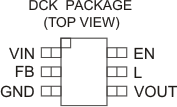
po_slvs776.gif

Pin Functions

PIN I/O DESCRIPTION
NAME NO.
EN 6 I Enable input (1: enabled, 0: disabled). Must be actively tied high or low. Do not leave floating.
FB 2 I Voltage feedback of adjustable version. Must be connected to VOUT at fixed output voltage versions.
GND 3 Control / logic and power ground
L 5 I Connection for Inductor
VIN 1 I Boost converter input voltage
VOUT 4 O Boost converter output voltage