SLVSB35C October 2012 – July 2015 TPS62175 , TPS62177
PRODUCTION DATA.
- 1 Features
- 2 Applications
- 3 Description
- 4 Revision History
- 5 Device Comparison Table
- 6 Pin Configuration and Functions
- 7 Specifications
- 8 Detailed Description
-
9 Application and Implementation
- 9.1 Application Information
- 9.2 Typical Application
- 9.3 System Examples
- 10Power Supply Recommendations
- 11Layout
- 12Device and Documentation Support
- 13Mechanical, Packaging, and Orderable Information
パッケージ・オプション
デバイスごとのパッケージ図は、PDF版データシートをご参照ください。
メカニカル・データ(パッケージ|ピン)
- DQC|10
サーマルパッド・メカニカル・データ
発注情報
9 Application and Implementation
NOTE
Information in the following applications sections is not part of the TI component specification, and TI does not warrant its accuracy or completeness. TI’s customers are responsible for determining suitability of components for their purposes. Customers should validate and test their design implementation to confirm system functionality.
9.1 Application Information
The TPS6217x is a high-efficiency synchronous step-down DC-DC converter, based on the DCS-Control topology.
With a wide operating input voltage range of 4.75 V to 28 V, the device is ideally suited for systems powered from multi cell Li-Ion as well as 12 V and even higher intermediate supply rails, providing up to 500-mA output current.
9.2 Typical Application
 Figure 8. Adjustable 0.5-A Power Supply
9.2.1 Design Requirements
The device operates for an input voltage range of 4.75 V to 28 V. The output voltage is adjustable, using an external resistive divider, or internally fixed.
The graphs were generated using the setup according to Figure 8. Table 1 shows the list of components used for the setup.
9.2.2 Detailed Design Procedures
Table 1. List of Components
| REFERENCE | DESCRIPTION | MANUFACTURER |
|---|---|---|
| IC | 28 V, 0.5-A Step-Down Converter, WSON | TPS62175DQC, Texas Instruments |
| L1 | 10 uH, (4 × 4 × 1.2) mm | LPS4012, Coilcraft |
| Cin | 2.2 µF, 50 V, Ceramic, 0805, X5R | Standard |
| Cout | 22 µF, 6.3 V, Ceramic, 0805, X5R | Standard |
| R1 | depending on VOUT | |
| R2 | depending on VOUT | |
| R3 | 100 kΩ, Chip, 0603, 1/16 W, 1% | Standard |
9.2.2.1 Programming the Output Voltage
While the output voltage of the TPS62175 is adjustable, the TPS62177 is programmed to a fixed output voltage of 3.3 V. For the fixed output voltage version, the FB pin is pulled low internally by a 400-kΩ resistor. TI recommends connecting the FB pin to AGND to improve thermal resistance. The adjustable version can be programmed for output voltages from 1 V to 6 V by using a resistive divider. The voltage at the FB pin is regulated to 800 mV. The value of the output voltage is set by the selection of the resistive divider from Equation 5. TI recommends choosing resistor values that allow a current of at least 5 uA. Lower resistor values are recommended to increase noise immunity. For applications requiring lowest current consumption, the use of the fixed-output voltage version is recommended.

As a safety feature, the device clamps the output voltage at the VOS pin to typically 7.4 V, if the FB pin gets opened.
9.2.2.2 External Component Selection
The external components must fulfill the needs of the application, but also the stability criteria of the device's control loop. The TPS6217x is optimized to work within a wide range of external components. The LC output filter's inductance and capacitance must be considered together, creating a double pole that is responsible for the corner frequency of the converter. Table 2 shows the recommended output filter components.
Table 2. Recommended LC Output Filter Combinations(1)
| 10 µF | 22 µF | 47 µF | 100 µF | 200 µF | 400 µF | |
|---|---|---|---|---|---|---|
| 6.8 µH | ||||||
| 10 µH | √(2) | √ | √ | √ | ||
| 22 µH | √ | √ | ||||
| 33 µH |
9.2.2.2.1 Output Filter and Loop Stability
The TPS6217x devices are internally compensated and are stable with LC output filter combinations recommended in Table 2. Further information on other values and loop stability can be found in Optimizing the TPS62175 Output Filter (SLVA543).
9.2.2.2.2 Inductor Selection
The inductor selection is determined by several effects like inductor ripple current, output ripple voltage, PWM-to-Power Save Mode transition point and efficiency. In addition, the inductor selected must be rated for appropriate saturation current and DC resistance (DCR). Equation 6 and Equation 7 calculate the maximum inductor current under static load conditions.

spacing
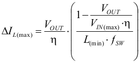
where
- ΔIL is the peak to peak inductor ripple current
- η is the converter efficiency (see efficiency figures)
- L(min) is the minimum inductor value
- fSW is the actual PWM switching frequency
Calculating the maximum inductor current using the actual operating conditions gives the minimum saturation current of the inductor needed. TI recommends a margin of about 20% to cover possible load transient overshoot. A larger inductor value is also useful to get lower ripple current, but increases the transient response time and solution size as well. The inductors listed in Table 3 have been tested with the TPS6217x.
Table 3. List of Inductors
| TYPE | INDUCTANCE (µH]) | CURRENT (A)(1) | DCR (mΩ) | DIMENSIONS (LENGTH x WIDTH x HEIGHT) mm | MANUFACTURER |
|---|---|---|---|---|---|
| LPS4012-103MLC | 10 µH, ±20% | 1.1 | 350 (maximum) | 4 x 4 × 1.2 | Coilcraft |
| LPS4018-103MLC | 10 µH, ±20% | 1.3 | 200 (maximum) | 4 x 4 × 1.8 | Coilcraft |
| VLS4012ET-100M | 10 µH, ±20% | 0.99 | 190 (typical) | 4 x 4 × 1.2 | TDK |
| VLCF4020T-100MR85 | 10 µH, ±20% | 0.85 | 168 (typical) | 4 × 4 × 2 | TDK |
| 74437324100 | 10 µH, ±20% | 1.5 | 215 (typical) | 4.5 × 4.1 × 1.8 | Wuerth |
| 744025100 | 10 µH, ±20% | 1 | 190 (maximum) | 2.8 × 2.8 × 2.8 | Wuerth |
| IFSC-1515AH-01 | 10 µH, ±20% | 1.3 | 135 (typical) | 3.8 × 3.8 × 1.8 | Vishay |
| ELL-4LG100MA | 10 µH, ±20% | 0.8 | 200 (typical) | 3.8 × 3.8 × 1.8 | Panasonic |
9.2.2.2.3 Output Capacitor Selection
The recommended value for the output capacitor is 22 uF. To maintain low output voltage ripple during large load transients, for output voltages less than 2 V, TI recommends 2 × 22 µF output capacitors. The architecture of the TPS6217x allows the use of ceramic output capacitors with low equivalent series resistance (ESR). These capacitors provide low output voltage ripple and are recommended with an X7R or X5R dielectric. Larger capacitance values have the advantage of smaller output voltage ripple and a tighter DC output accuracy in power save mode.
NOTE
In power save mode, the output voltage ripple and accuracy depends on the output capacitance and the inductor value. The larger the capacitance the lower the output voltage ripple and the better the output voltage accuracy. The same relation applies to the inductor value.
9.2.2.2.4 Input Capacitor Selection
Typically, 2.2 µF is sufficient and is recommended, though a larger value reduces input current ripple further. The input capacitor buffers the input voltage during transient events and also decouples the converter from the supply. TI recommends a low ESR, multilayer, X5R or X7R dielectric, ceramic capacitor for best filtering, which should be placed between VIN and PGND as close as possible to those pins.
spacing
spacing
spacing
NOTE
DC Bias effect: High capacitance ceramic capacitors have a DC Bias effect, which has a strong influence on the final effective capacitance. Therefore, the right capacitor value must be chosen carefully. Package size and voltage rating in combination with dielectric material are responsible for differences between the rated capacitor value and the effective capacitance.
9.2.3 Application Curves
VIN=12 V, VOUT = 3.3 V, TJ=25°C, unless otherwise noted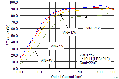
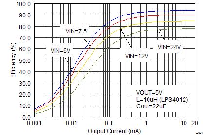
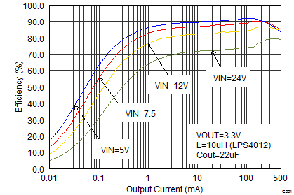
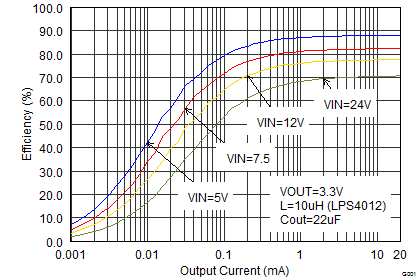
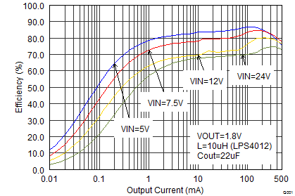
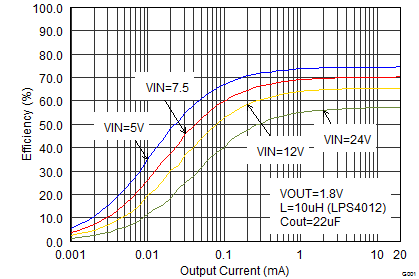
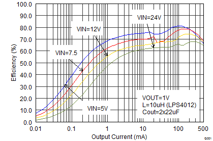
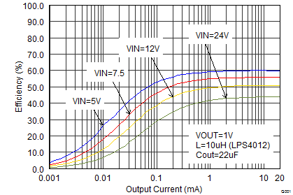
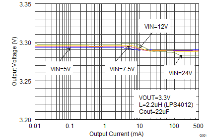
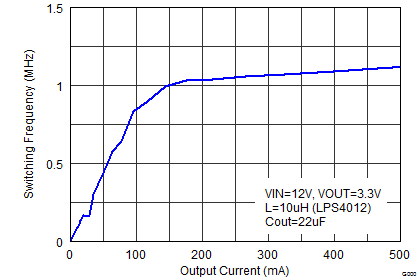
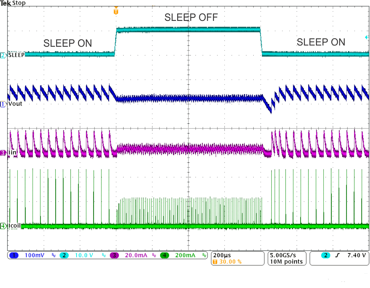 Figure 31. Sleep Mode Entry/Exit, IOUT = 10 mA
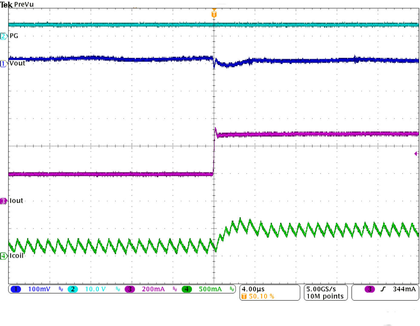 Figure 33. Load Transient Response, PWM Mode, IOUT (200 mA to 500 mA), Rising Edge
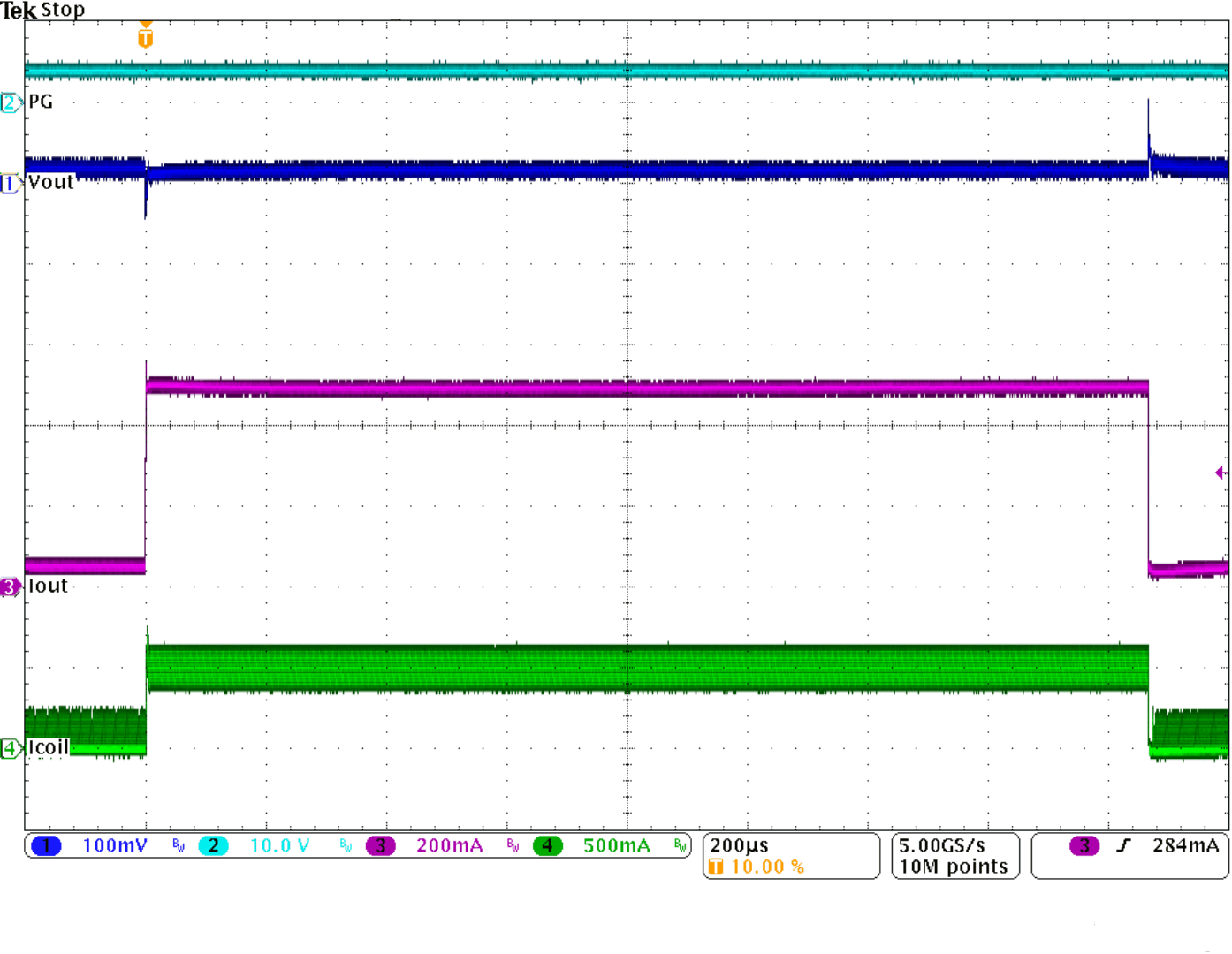 Figure 35. Load Transient Response, Power Save Mode, IOUT (50 mA to 500 mA)
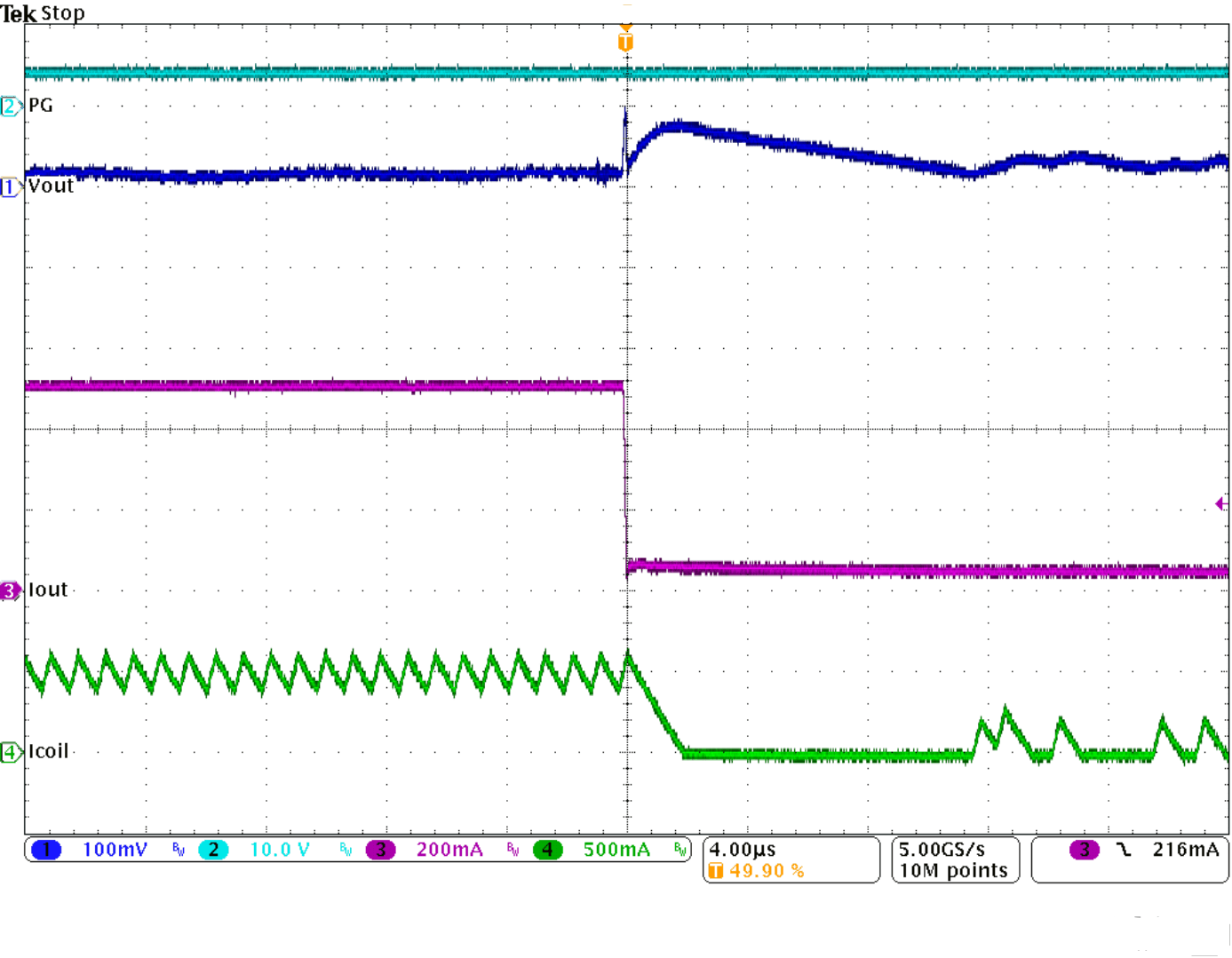 Figure 37. Load Transient Response, Power Save Mode, IOUT (50 mA to 500 mA), Falling Edge
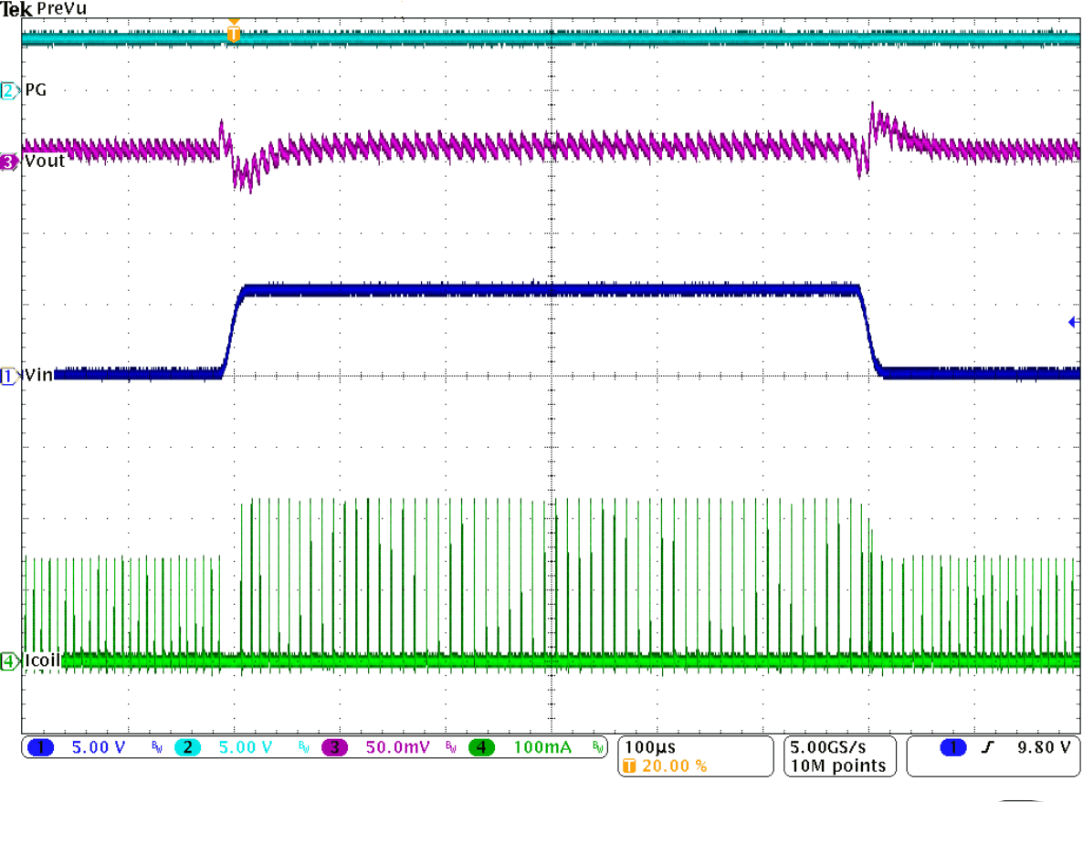
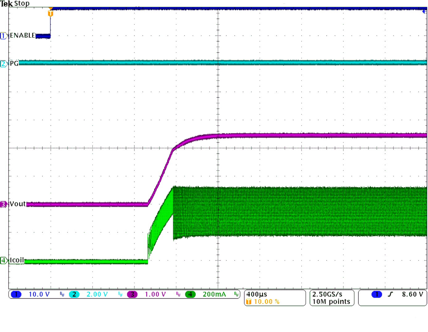 Figure 41. Start-Up Current Limit, RLOAD = 6.6 Ω
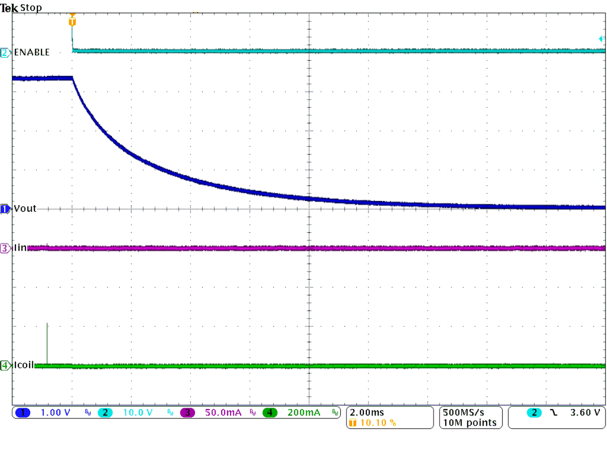
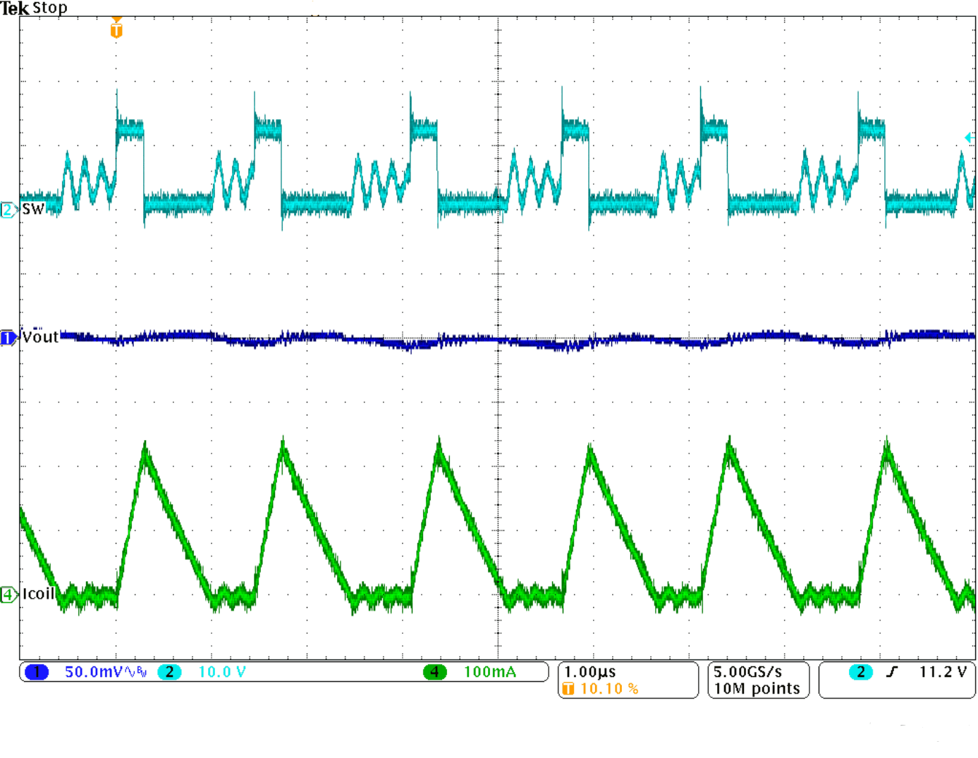 Figure 45. Typical Operation in Power Save Mode, IOUT = 75 mA
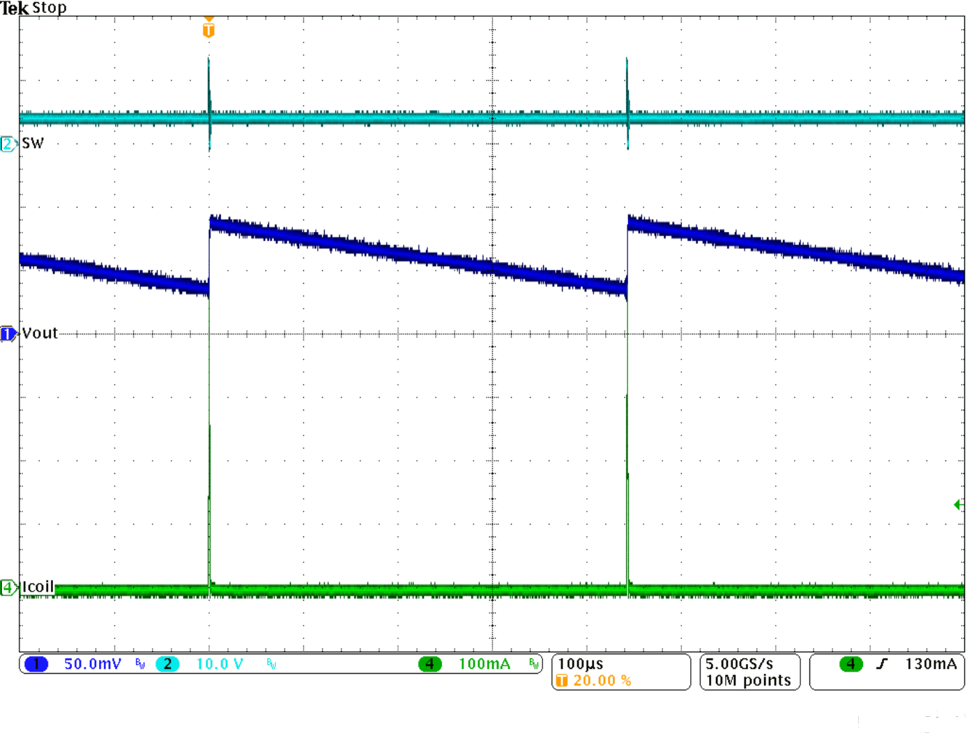 Figure 47. Typical Operation in Sleep Mode, IOUT = 1 mA
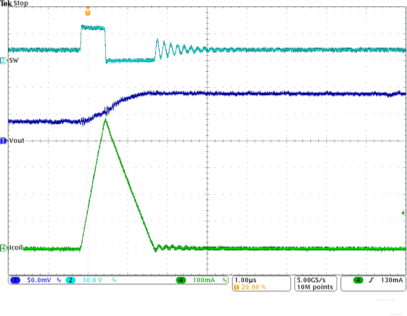 Figure 49. Typical Operation in Sleep Mode, IOUT = 1 mA (Single Pulse)
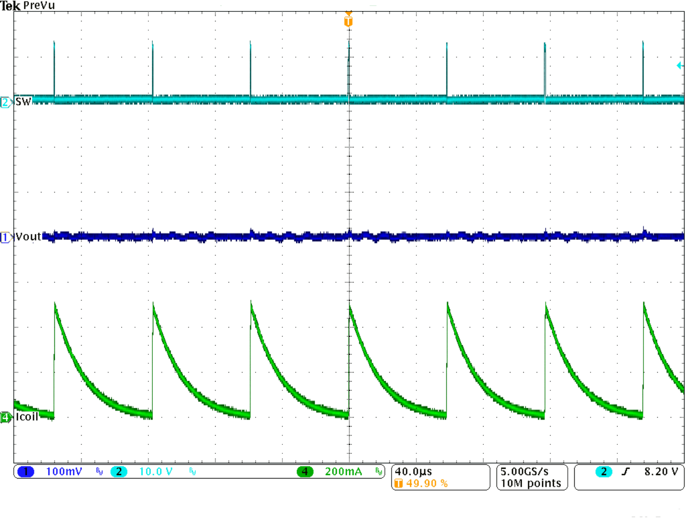 Figure 51. Short Circuit From Start-Up
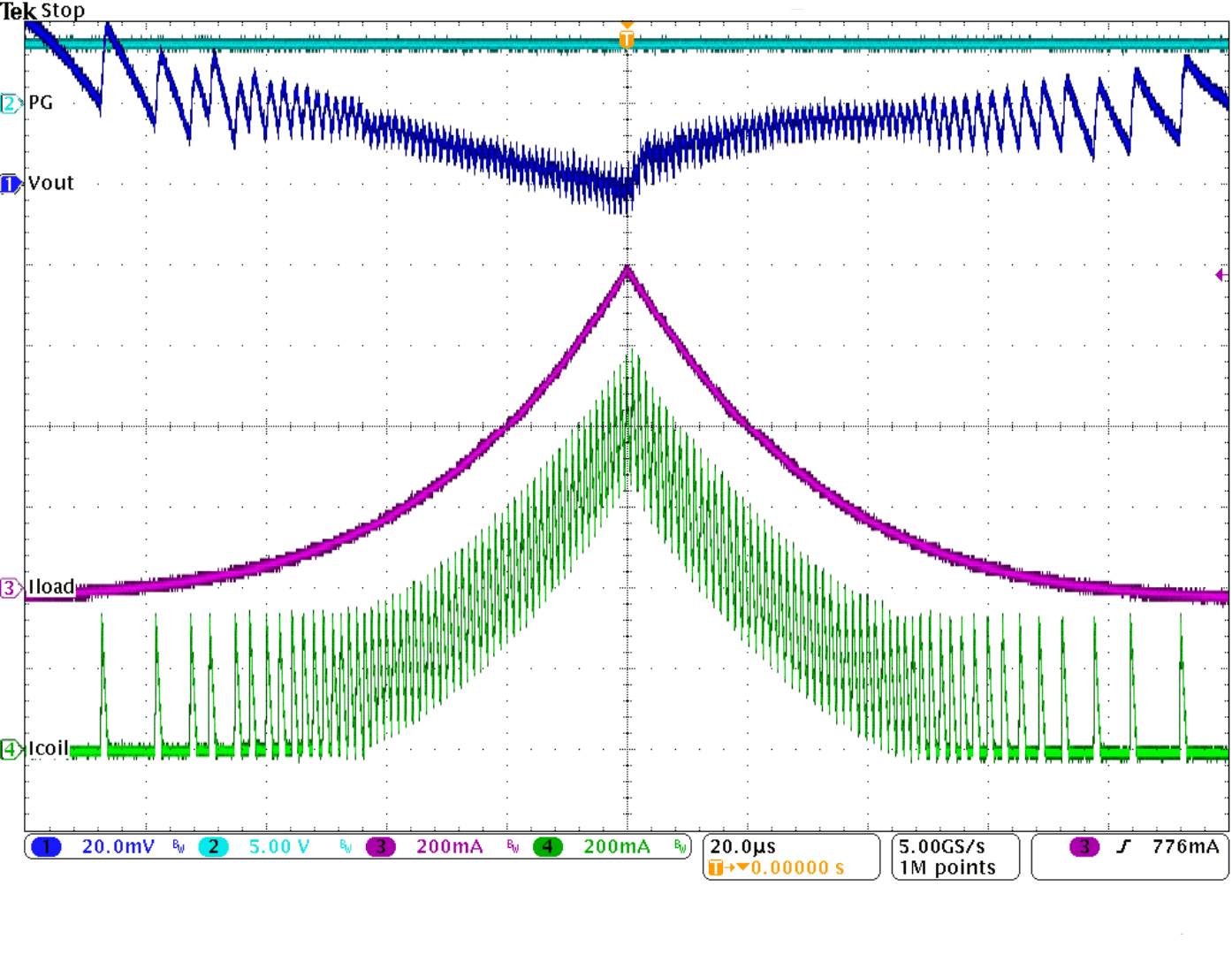 Figure 53. Triangular Load Sweep With Mode Transitions (Power Save Mode - PWM Mode - Power Save Mode), VIN = 24 V
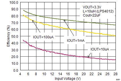
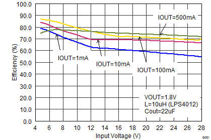
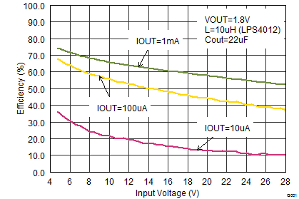
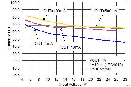
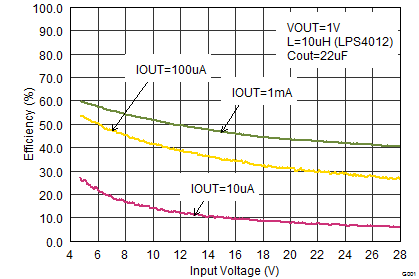
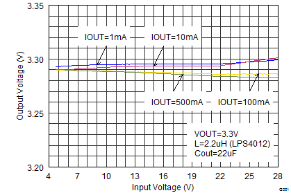
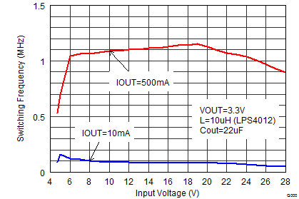
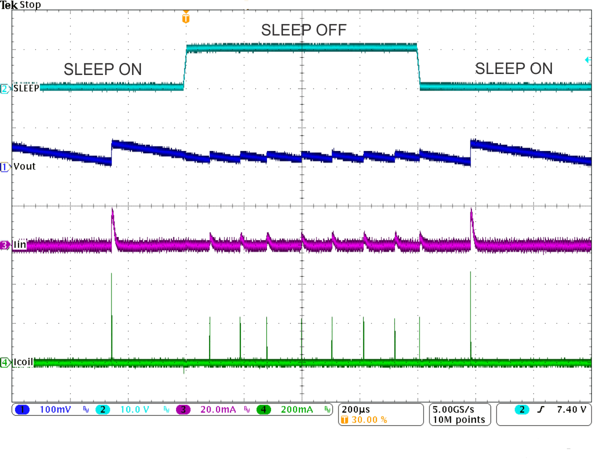 Figure 30. Sleep Mode Entry/Exit, IOUT = 1 mA
 Figure 32. Load Transient Response, PWM Mode, IOUT (200 mA to 500 mA)
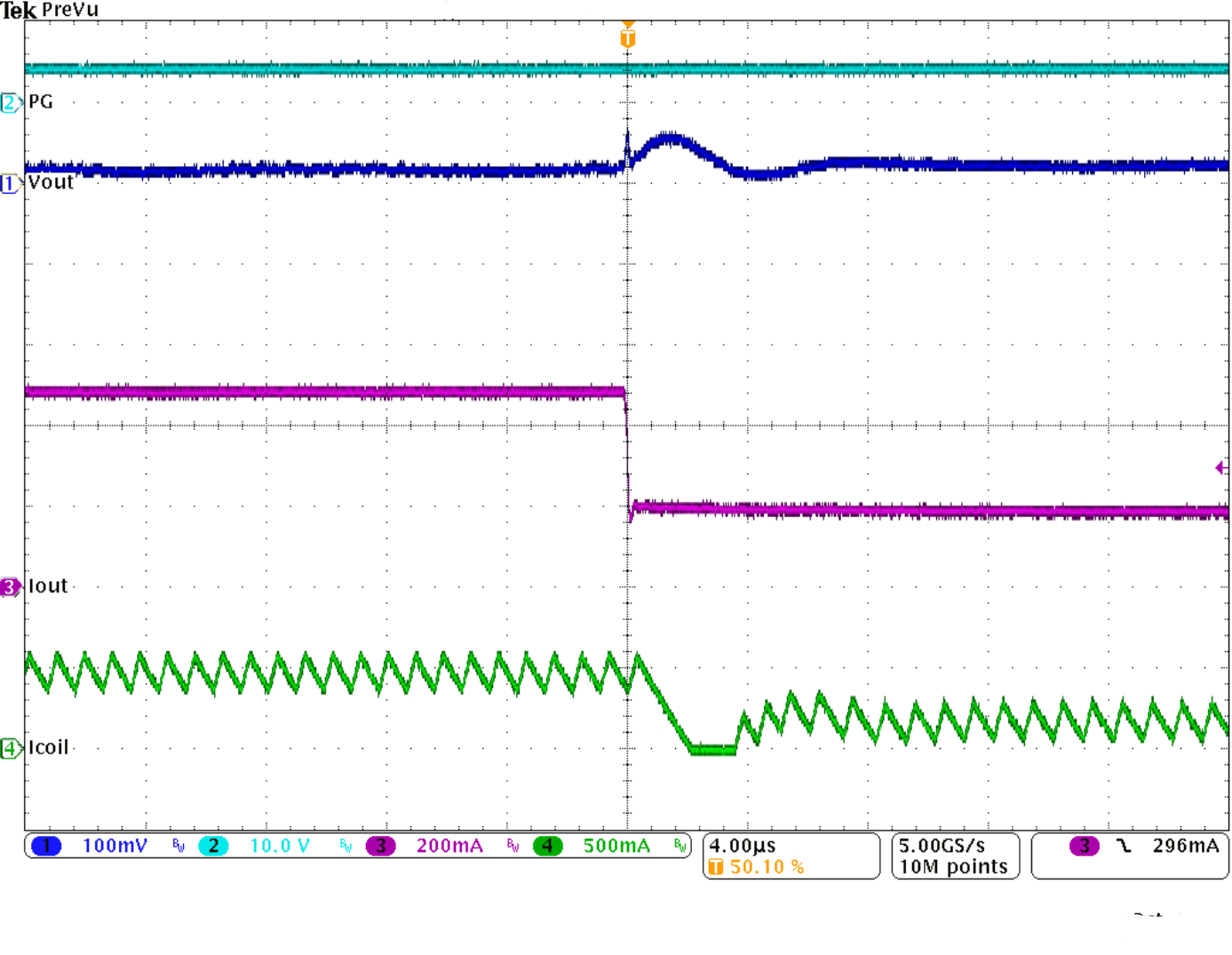 Figure 34. Load Transient Response, PWM Mode, IOUT (200 mA to 500 mA), Falling Edge
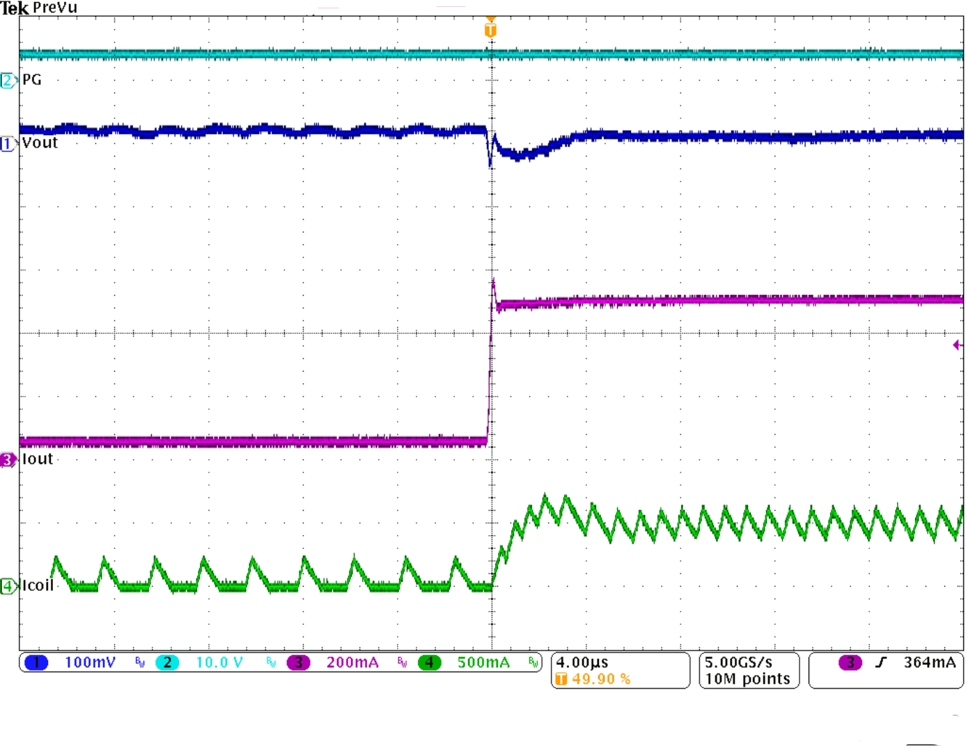 Figure 36. Load Transient Response, Power Save Mode, IOUT (50 mA to 500 mA), Rising Edge
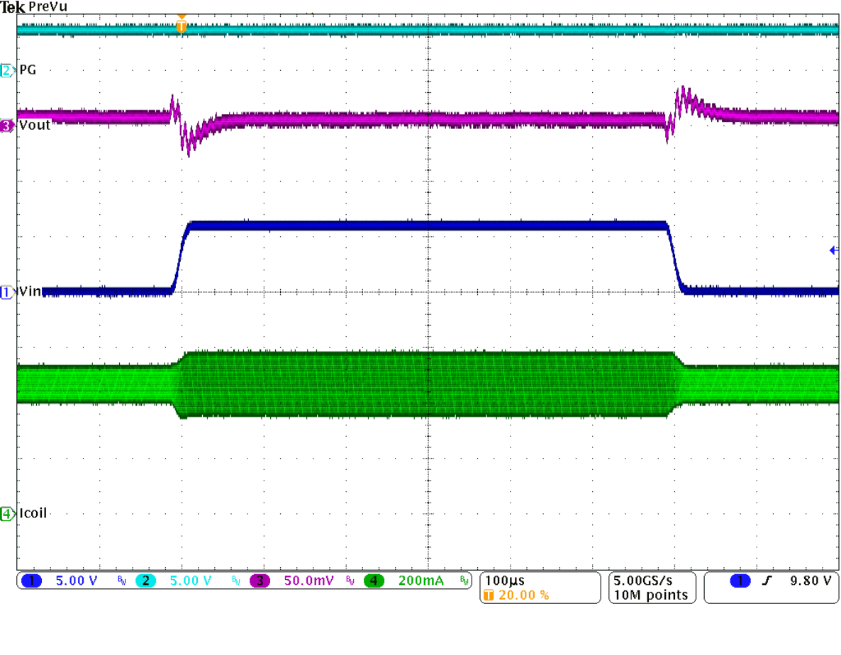
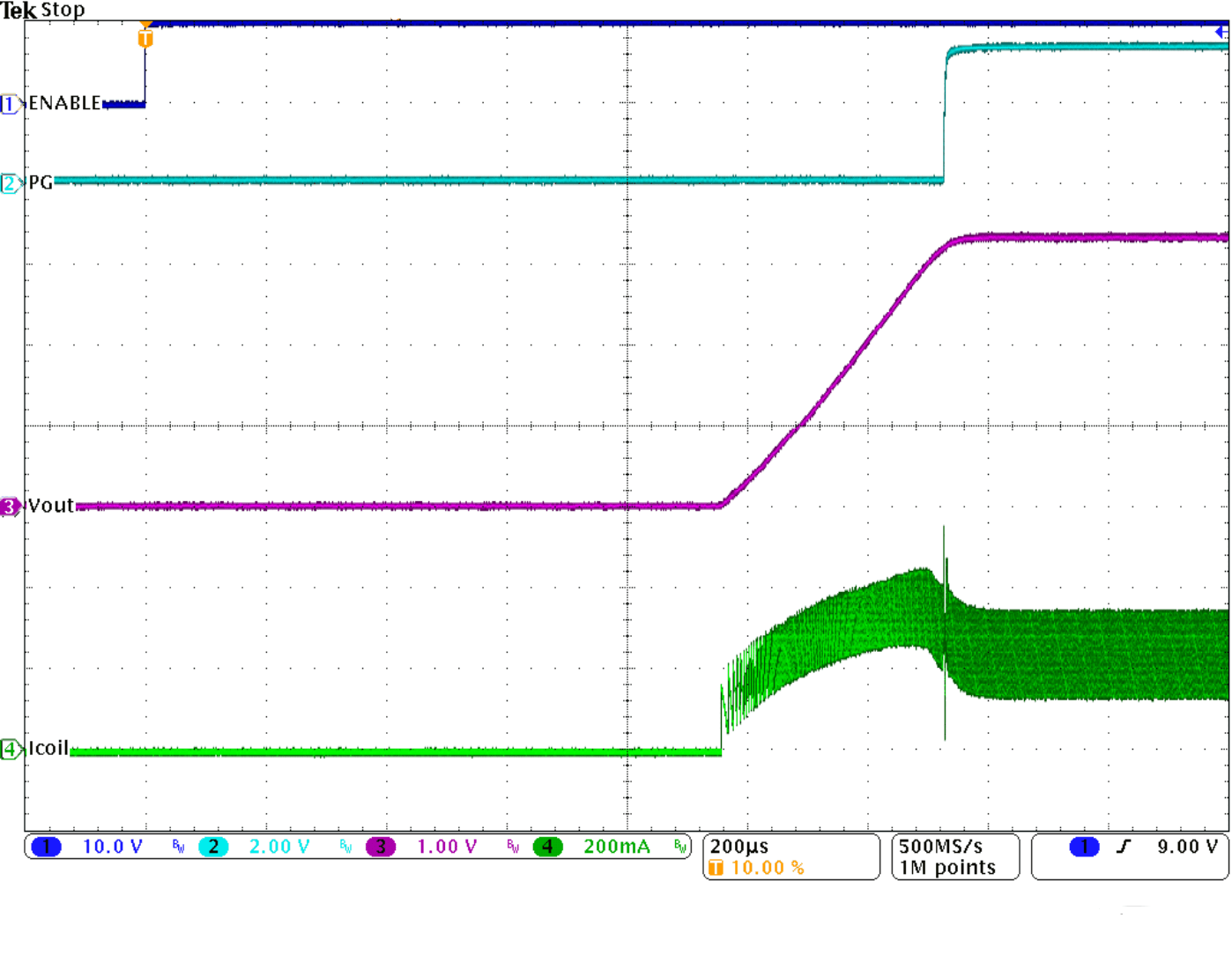 Figure 40. Start-Up (PWM Mode), IOUT = 250 mA
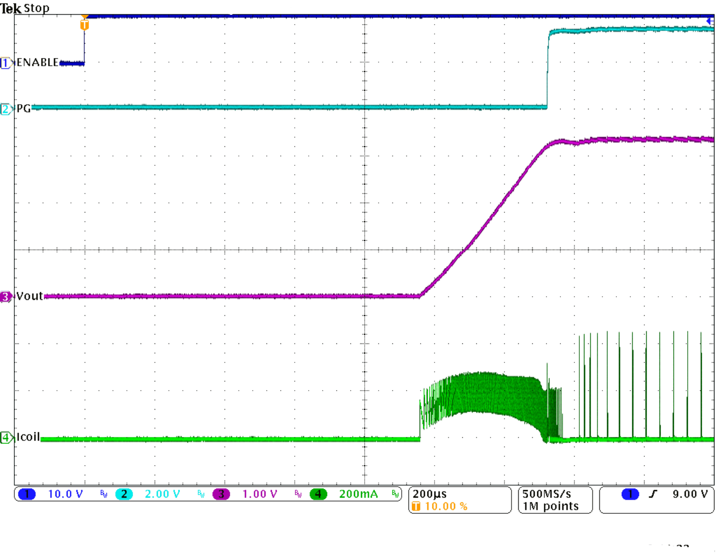 Figure 42. Start-Up (Sleep Mode), IOUT = 10 mA
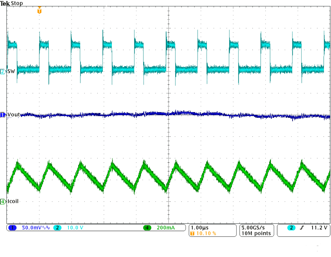 Figure 44. Typical Operation in PWM Mode, IOUT = 250 mA
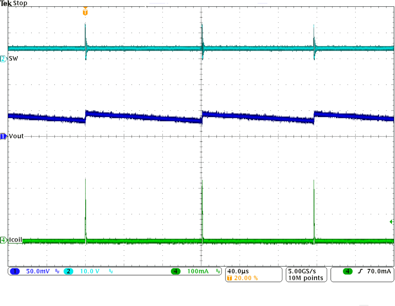 Figure 46. Typical Operation in Power Save Mode, IOUT = 1 mA
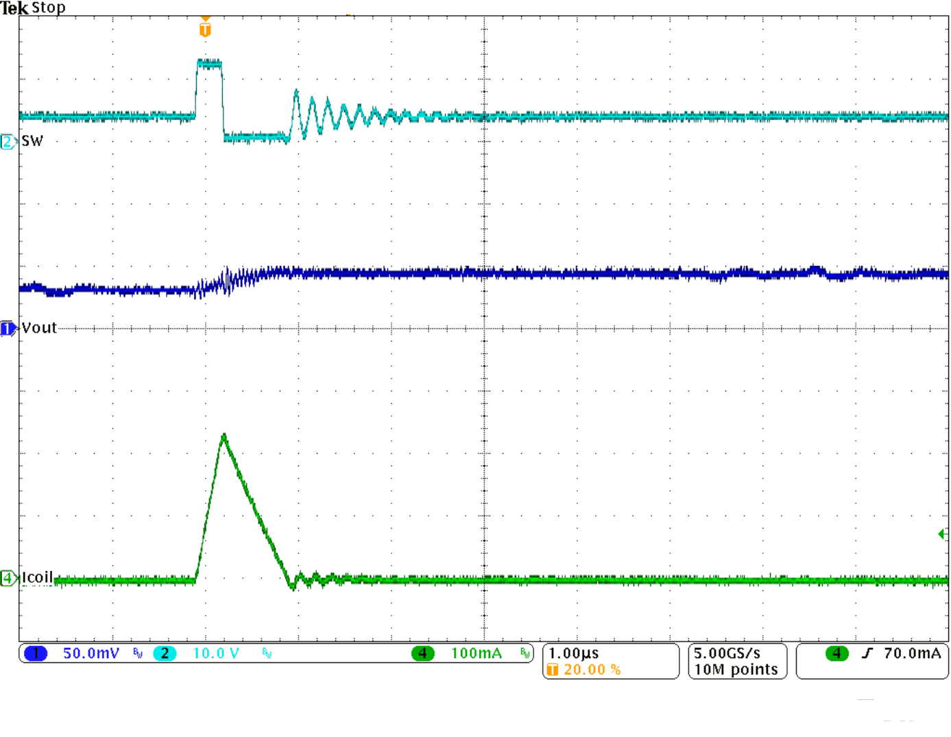 Figure 48. Typical Operation in Power Save Mode, IOUT = 1 mA (Single Pulse)
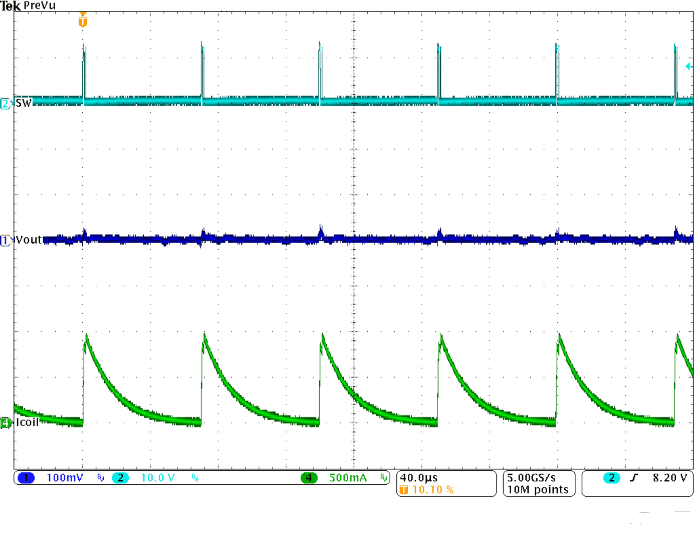 Figure 50. Short Circuit While Running
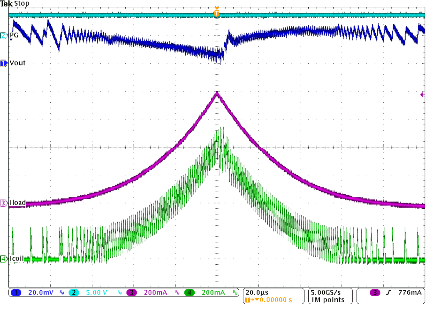 Figure 52. Triangular Load Sweep With Mode Transitions (Power Save Mode - PWM Mode - Power Save Mode)
9.3 System Examples
9.3.1 Microcontroller Power Supply
The TPS6217x can be used advantageously as the power supply rail for microcontrollers with low current power save modes. Figure 54 shows the connection of TPS62177 to the Tiva C Series TM4C123x ARM Cortex™ - M4 MCUs (TM4C123x MCUs), using its hibernate mode signal to control sleep mode operation. More information is found in the Application Report, Powering Tiva™ C Series Microcontrollers Using the High Efficiency DCS-Control™ Topology (SPMA066).
spacing
spacing
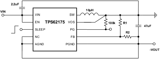
9.3.2 Inverting Power Supply
The TPS6217x can be used as inverting power supply by rearranging external circuitry as shown in Figure 55. As the former GND node now represents a voltage level below system ground, the voltage difference between VIN and VOUT must be limited to the maximum operating voltage of 28 V.
spacing
spacing
More information about using TPS62175 as inverting buck-boost converter can be found in the Application Note, Using the TPS62175 in an Inverting Buck Boost Topology (SLVA542).
9.3.3 TPS62175 Adjustable Output Voltages
The following example circuits show typical schematics for commonly used output voltage values using the adjustable device version TPS62175.
9.3.3.1 5-V / 0.5-A Power Supply
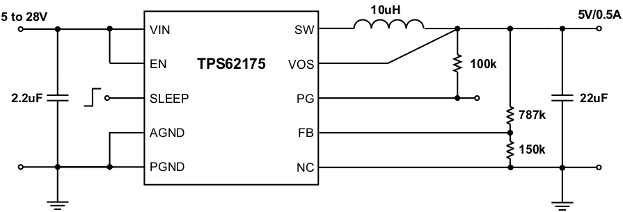 Figure 56. 5-V / 0.5-A Power Supply
9.3.3.2 2.5-V / 0.5-A Power Supply
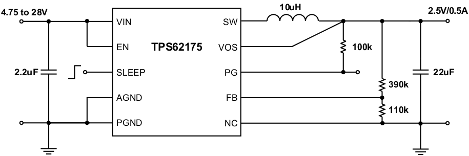 Figure 57. 2.5-V / 0.5-A Power Supply
9.3.3.3 1.8-V / 0.5-A Power Supply
 Figure 58. 1.8-V / 0.5-A Power Supply
9.3.3.4 1.2-V / 0.5-A Power Supply
 Figure 59. 1.2-V / 0.5-A Power Supply
9.3.3.5 1-V / 0.5-A Power Supply
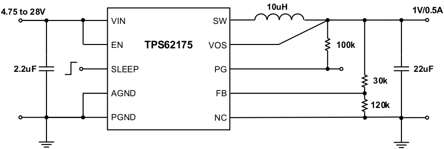 Figure 60. 1-V / 0.5-A Power Supply
9.3.4 TPS62177 Fixed 3.3-V / 0.5-A Power Supply
The following example circuit shows the typical schematic for fixed output voltage using the device version TPS62177.
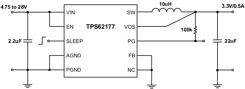 Figure 61. 3.3-V / 0.5-A Power Supply

