SLVS737A February 2007 – July 2015 TPS62410
PRODUCTION DATA.
- 1 Features
- 2 Applications
- 3 Description
- 4 Revision History
- 5 Pin Configuration and Functions
- 6 Specifications
- 7 Detailed Description
- 8 Application and Implementation
- 9 Power Supply Recommendations
- 10Layout
- 11Device and Documentation Support
- 12Mechanical, Packaging, and Orderable Information
1 Features
- High Efficiency up to 95%
- VIN Range from 2.5 V to 6 V
- 2.25-MHz Fixed Frequency Operation
- Output Current 2 x 800 mA
- Adjustable Output Voltage from 0.6 V to VIN
- Optional EasyScale™ One-Pin Serial Interface for Dynamic Output Voltage Adjustment
- Power-Save Mode at Light Load Currents
- 180° Out of Phase Operation
- Output Voltage Accuracy in PWM Mode ±1%
- Typical 32-μA Quiescent Current for Both Converters
- 100% Duty Cycle for Lowest Dropout
- Available in a 10-Pin VSON (3 mm × 3 mm)
2 Applications
- Cell Phones, Smartphones
- PDAs, Pocket PCs
- OMAP™ and Low-Power DSP Supply
- Portable Media Players
- Digital Radios
- Digital Cameras
3 Description
The TPS62410 device is a synchronous dual step-down DC–DC converter. It provides two independent output voltage rails powered by 1-cell Li-Ion or 3-cell NiMH/NiCD batteries. The device is also suitable to operate from a standard 3.3 V or 5 V voltage rail.
With an input voltage range of 2.5 V to 6 V, the TPS62410 is ideal for battery powered portable applications like smart phones, PDAs, and other portable equipment.
With the EasyScale™ serial interface, the output voltages can be modified during operation. It therefore supports dynamic voltage scaling for low-power DSP and processors.
The TPS62410 operates at 2.25-MHz fixed switching frequency and enter the power-save mode operation at light load currents to maintain high efficiency over the entire load current range. For low-noise applications the devices can be forced into fixed frequency PWM mode by pulling the MODE/DATA pin High. In the shutdown mode, the current consumption is reduced to 1.2 μA. The device allows the use of small inductors and capacitors to achieve a small solution size.
The TPS62410 operates over a free-air temperature range of –40°C to 85°C. It is available in a 10-pin leadless package (3 × 3 mm VSON)
Device Information(1)
| PART NUMBER | PACKAGE | BODY SIZE (NOM) |
|---|---|---|
| TPS62410 | VSON (10) | 3.00 mm × 3.00 mm |
- For all available packages, see the orderable addendum at the end of the data sheet.
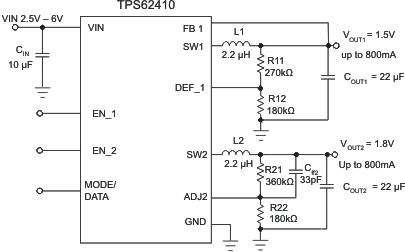
Typical Application Schematic

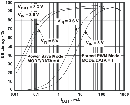
Efficiency vs Output Current
