JAJSF01I November 2011 – March 2018 TPS65217
PRODUCTION DATA.
- 1 特長
- 2 アプリケーション
- 3 概要
- 4 改訂履歴
- 5 Device Comparison Table
- 6 Pin Configuration and Functions
- 7 Specifications
-
8 Detailed Description
- 8.1 Overview
- 8.2 Functional Block Diagram
- 8.3
Feature Description
- 8.3.1 Wake-Up and Power-Up Sequencing
- 8.3.2 Power Good
- 8.3.3 Push-Button Monitor (PB_IN)
- 8.3.4 nWAKEUP Pin (nWAKEUP)
- 8.3.5 Power Enable Pin (PWR_EN)
- 8.3.6 Reset Pin (nRESET)
- 8.3.7 Interrupt Pin (nINT)
- 8.3.8 Analog Multiplexer
- 8.3.9 Battery Charger and Power Path
- 8.3.10 Battery Charging
- 8.3.11 Precharge
- 8.3.12 Charge Termination
- 8.3.13 Battery Detection and Recharge
- 8.3.14 Safety Timer
- 8.3.15 Battery-Pack Temperature Monitoring
- 8.3.16 DC/DC Converters
- 8.3.17 Standby LDO Regulators (LDO1, LDO2)
- 8.3.18 Load Switches or LDO Regulators (LS1 or LDO3, LS2 or LDO4)
- 8.3.19 White LED Driver
- 8.4 Device Functional Modes
- 8.5 Programming
- 8.6
Register Maps
- 8.6.1 Register Address Map
- 8.6.2 Chip ID Register (CHIPID) (Address = 0x00) [reset = X]
- 8.6.3 Power Path Control Register (PPATH) (Address = 0x01) [reset = 0x3D]
- 8.6.4 Interrupt Register (INT) (Address = 0x02) [reset = 0x80]
- 8.6.5 Charger Configuration Register 0 (CHGCONFIG0) (Address = 0x03) [reset = 0x00]
- 8.6.6 Charger Configuration Register 1 (CHGCONFIG1) (Address = 0x04) [reset = 0xB1]
- 8.6.7 Charger Configuration Register 2 (CHGCONFIG2) (Address = 0x05) [reset = 0x80]
- 8.6.8 Charger Configuration Register 3 (CHGCONFIG3) (Address = 0x06) [reset = 0xB2]
- 8.6.9 WLED Control Register 1 (WLEDCTRL1) (Address = 0x07) [reset = 0xB1]
- 8.6.10 WLED Control Register 2 (WLEDCTRL2) (Address = 0x08) [reset = 0x00]
- 8.6.11 MUX Control Register (MUXCTRL) (Address = 0x09) [reset = 0x00]
- 8.6.12 Status Register (STATUS) (Address = 0x0A) [reset = 0x00]
- 8.6.13 Password Register (PASSWORD) (Address = 0x0B) [reset = 0x00]
- 8.6.14 Power Good Register (PGOOD) (Address = 0x0C) [reset = 0x00]
- 8.6.15 Power-Good Control Register (DEFPG) (Address = 0x0D) [reset = 0x0C]
- 8.6.16 DCDC1 Control Register (DEFDCDC1) (Address = 0x0E) [reset = X]
- 8.6.17 DCDC2 Control Register (DEFDCDC2) (Address = 0x0F) [reset = X]
- 8.6.18 DCDC3 Control Register (DEFDCDC3) (Address = 0x10) [reset = 0x08]
- 8.6.19 Slew-Rate Control Register (DEFSLEW) (Address = 0x11) [reset = 0x06]
- 8.6.20 LDO1 Control Register (DEFLDO1) (Address = 0x12) [reset = 0x09]
- 8.6.21 LDO2 Control Register (DEFLDO2) (Address = 0x13) [reset = 0x38]
- 8.6.22 Load Switch1 or LDO3 Control Register (DEFLS1) (Address = 0x14) [reset = X]
- 8.6.23 Load Switch2 or LDO4 Control Register (DEFLS2) (Address = 0x15) [reset = X]
- 8.6.24 Enable Register (ENABLE) (Address = 0x16) [reset = 0x00]
- 8.6.25 UVLO Control Register (DEFUVLO) (Address = 0x18) [reset = 0x03]
- 8.6.26 Sequencer Register 1 (SEQ1) (Address = 0x19) [reset = X]
- 8.6.27 Sequencer Register 2 (SEQ2) (Address = 0x1A) [reset = X]
- 8.6.28 Sequencer Register 3 (SEQ3) (Address = 0x1B) [reset = X]
- 8.6.29 Sequencer Register 4 (SEQ4) (Address = 0x1C) [reset = 0x40]
- 8.6.30 Sequencer Register 5 (SEQ5) (Address = 0x1D) [reset = X]
- 8.6.31 Sequencer Register 6 (SEQ6) (Address = 0x1E) [reset = 0x00]
- 9 Application and Implementation
- 10Power Supply Recommendations
- 11Layout
- 12デバイスおよびドキュメントのサポート
- 13メカニカル、パッケージ、および注文情報
パッケージ・オプション
メカニカル・データ(パッケージ|ピン)
- RSL|48
サーマルパッド・メカニカル・データ
- RSL|48
発注情報
9.2.2.2 5-V Operation Without a Battery
The TPS65217x device has a linear charger for Li+ batteries, and TI recommends that a battery is included in designs for ideal performance. However, the device can operate without a battery attached. Three basic use cases are available for operation without a battery:
- The system is designed for battery operation, but the battery is removable and the end user does not have the battery inserted. The system can be powered by connecting an AC adaptor or USB supply.
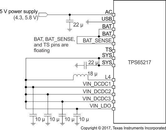
- A nonportable system operates on a (regulated) 5-V supply, but the PMIC must provide protection against input overvoltage up to 20 V. Electrically, this case is the same as the previous case where the device is powered by an AC adaptor. The battery pins (BAT and BATSENSE) are shorted together and floating, the temperature sensing pin (TS) is left floating, and power is provided through the AC pin. The DC/DC converters, the WLED driver, and the LDO regulators connect to the overvoltage-protected SYS pins. The load switches (or LDO3 and LDO4, depending on configuration) typically connect to one of the lower system rails, but can also be connected to the SYS pin.
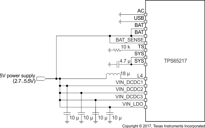
- A nonportable system operates on a regulated 5-V supply that does not require input overvoltage protection. In this case, the 5-V power supply is connected through the BAT pins. The DC/DC converter inputs, WLED driver, LDO1, and LDO2 are connected directly to the 5-V supply. A standard, constant-value 10-kΩ resistor is connected from the TS pin to ground to simulate the NTC thermistor monitoring the battery. The load switches (or LDO3 and LDO4, depending on configuration) typically connect to one of the lower system rails, but can also be connected directly to the 5-V input supply.
Figure 61 shows the connection of the input power supply to the device for 5-V only operation, with 20-V input overvoltage protection. Figure 62 shows the connection of the input power supply to the device for 5-V only operation without 20-V input overvoltage protection. Table 37 lists the functional differences between both setups.

The SYS node and DC/DC converters are protected against input overvoltage up to 20 V.
Figure 61. Power Connection for 5-V Only Operation With OVP, Without a Battery 
1. The DC/DC converters are not protected against input overvoltage.
Figure 62. Power Connection for 5-V Only Operation Directly Wired to BAT Instead of a Battery Table 37. Functional Differences Between 5-V Only Operation Without a Battery and With and Without 20-V Input Overvoltage Protection
| RESOURCE IMPACTED | POWER SUPPLIED THROUGH AC PIN
(CASE (1) AND (2)) |
POWER SUPPLIED THROUGH BAT PIN
(CASE (3)) |
|---|---|---|
| Input protection | The maximum operating input voltage is 5.8 V, but the device is protected from input overvoltage up to 20 V. | The maximum operating input voltage is 5.5 V. |
| Power efficiency | The input current for DC/DC converters passes through AC-SYS power-path switch (approximately 150 mΩ). | The internal power path is bypassed to minimize I2R losses. |
| BATTEMP bit | The BATTEMP bit (bit 0 in register 0x03) always reads 1, but has no effect on operation of the device. | The BATTEMP bit (bit 0 in register 0x03) always reads 0. |
| Output rail status on initial power connection | The LDO1 regulator is automatically powered up when the AC pin is connected to the 5-V supply, and the device goes to the WAIT PWR_EN state. If the PWR_EN pin is not asserted within 5 s, the LDO1 regulator turns OFF. | The LDO1 regulator is OFF when the BAT pin is connected to the 5-V supply. The PB_IN pin must be pulled low to go to the WAIT PWR_EN state. The PB_IN pin cannot stay low for greater than 8 s or a reset will occur. |
| Response to input overvoltage | Device goes to the OFF state.(1) | Not applicable |
| Power path | In an application with one source of input power, if the input power drops below UVLO and recovers before reaching 100 mV, the rising edge may not be detected by the device. This condition, known as a brownout, can cause a lockup of the device in which the I2C is responsive but SYS is not connected to the AC or USB through the power path. (2) | Not applicable |
(1) If a battery is present in the system, the TPS65217x device automatically switches from using the AC pin as the power supply to using BAT as the supply when the AC input exceeds 6.4 V. The device automatically switches back to supplying power from the AC pin when the AC input recovers and the voltages decreases to less than 5.8 V.
(2) As a workaround, supply power through the BAT input pin or change UVLO to 2.73 V by changing the UVLO[1:0] bits in register 0x18 to 00b. This setting must be changed during initialization after the first power-on event of the device. The bits return to the default value when all I2C registers reset. As a result, if a brownout condition can occur during the first power-on event, then external circuitry must be added to prevent the TPS65217x device from being affected by the brownout condition.