JAJSF01I November 2011 – March 2018 TPS65217
PRODUCTION DATA.
- 1 特長
- 2 アプリケーション
- 3 概要
- 4 改訂履歴
- 5 Device Comparison Table
- 6 Pin Configuration and Functions
- 7 Specifications
-
8 Detailed Description
- 8.1 Overview
- 8.2 Functional Block Diagram
- 8.3
Feature Description
- 8.3.1 Wake-Up and Power-Up Sequencing
- 8.3.2 Power Good
- 8.3.3 Push-Button Monitor (PB_IN)
- 8.3.4 nWAKEUP Pin (nWAKEUP)
- 8.3.5 Power Enable Pin (PWR_EN)
- 8.3.6 Reset Pin (nRESET)
- 8.3.7 Interrupt Pin (nINT)
- 8.3.8 Analog Multiplexer
- 8.3.9 Battery Charger and Power Path
- 8.3.10 Battery Charging
- 8.3.11 Precharge
- 8.3.12 Charge Termination
- 8.3.13 Battery Detection and Recharge
- 8.3.14 Safety Timer
- 8.3.15 Battery-Pack Temperature Monitoring
- 8.3.16 DC/DC Converters
- 8.3.17 Standby LDO Regulators (LDO1, LDO2)
- 8.3.18 Load Switches or LDO Regulators (LS1 or LDO3, LS2 or LDO4)
- 8.3.19 White LED Driver
- 8.4 Device Functional Modes
- 8.5 Programming
- 8.6
Register Maps
- 8.6.1 Register Address Map
- 8.6.2 Chip ID Register (CHIPID) (Address = 0x00) [reset = X]
- 8.6.3 Power Path Control Register (PPATH) (Address = 0x01) [reset = 0x3D]
- 8.6.4 Interrupt Register (INT) (Address = 0x02) [reset = 0x80]
- 8.6.5 Charger Configuration Register 0 (CHGCONFIG0) (Address = 0x03) [reset = 0x00]
- 8.6.6 Charger Configuration Register 1 (CHGCONFIG1) (Address = 0x04) [reset = 0xB1]
- 8.6.7 Charger Configuration Register 2 (CHGCONFIG2) (Address = 0x05) [reset = 0x80]
- 8.6.8 Charger Configuration Register 3 (CHGCONFIG3) (Address = 0x06) [reset = 0xB2]
- 8.6.9 WLED Control Register 1 (WLEDCTRL1) (Address = 0x07) [reset = 0xB1]
- 8.6.10 WLED Control Register 2 (WLEDCTRL2) (Address = 0x08) [reset = 0x00]
- 8.6.11 MUX Control Register (MUXCTRL) (Address = 0x09) [reset = 0x00]
- 8.6.12 Status Register (STATUS) (Address = 0x0A) [reset = 0x00]
- 8.6.13 Password Register (PASSWORD) (Address = 0x0B) [reset = 0x00]
- 8.6.14 Power Good Register (PGOOD) (Address = 0x0C) [reset = 0x00]
- 8.6.15 Power-Good Control Register (DEFPG) (Address = 0x0D) [reset = 0x0C]
- 8.6.16 DCDC1 Control Register (DEFDCDC1) (Address = 0x0E) [reset = X]
- 8.6.17 DCDC2 Control Register (DEFDCDC2) (Address = 0x0F) [reset = X]
- 8.6.18 DCDC3 Control Register (DEFDCDC3) (Address = 0x10) [reset = 0x08]
- 8.6.19 Slew-Rate Control Register (DEFSLEW) (Address = 0x11) [reset = 0x06]
- 8.6.20 LDO1 Control Register (DEFLDO1) (Address = 0x12) [reset = 0x09]
- 8.6.21 LDO2 Control Register (DEFLDO2) (Address = 0x13) [reset = 0x38]
- 8.6.22 Load Switch1 or LDO3 Control Register (DEFLS1) (Address = 0x14) [reset = X]
- 8.6.23 Load Switch2 or LDO4 Control Register (DEFLS2) (Address = 0x15) [reset = X]
- 8.6.24 Enable Register (ENABLE) (Address = 0x16) [reset = 0x00]
- 8.6.25 UVLO Control Register (DEFUVLO) (Address = 0x18) [reset = 0x03]
- 8.6.26 Sequencer Register 1 (SEQ1) (Address = 0x19) [reset = X]
- 8.6.27 Sequencer Register 2 (SEQ2) (Address = 0x1A) [reset = X]
- 8.6.28 Sequencer Register 3 (SEQ3) (Address = 0x1B) [reset = X]
- 8.6.29 Sequencer Register 4 (SEQ4) (Address = 0x1C) [reset = 0x40]
- 8.6.30 Sequencer Register 5 (SEQ5) (Address = 0x1D) [reset = X]
- 8.6.31 Sequencer Register 6 (SEQ6) (Address = 0x1E) [reset = 0x00]
- 9 Application and Implementation
- 10Power Supply Recommendations
- 11Layout
- 12デバイスおよびドキュメントのサポート
- 13メカニカル、パッケージ、および注文情報
パッケージ・オプション
メカニカル・データ(パッケージ|ピン)
- RSL|48
サーマルパッド・メカニカル・データ
- RSL|48
発注情報
8.3.15 Battery-Pack Temperature Monitoring
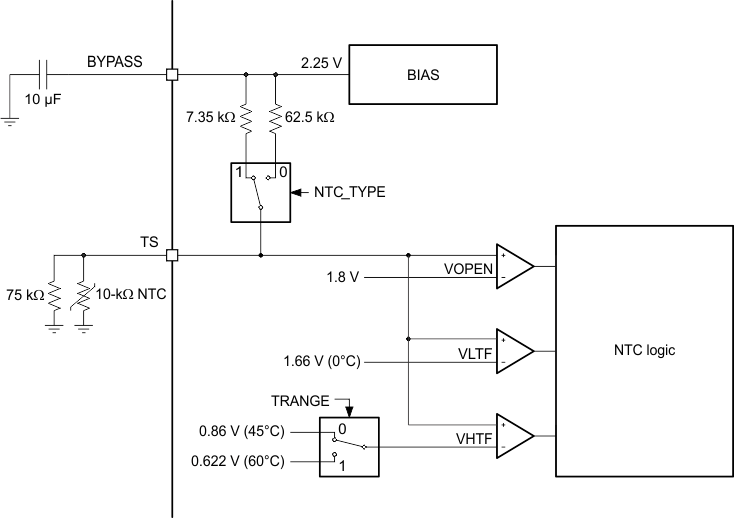
The TS pin of the TPS65217x device connects to the NTC resistor in the battery pack. During charging, if the NTC resistance indicates that battery operation is less than or greater than the limits of normal operation, charging is suspended and the safety timer value is paused and held at the present value. When the battery pack temperature returns to within the limits of normal operation, charging resumes and the safety time is started again without resetting.
By default, the device supports a 10-kΩ NTC resistor with a B-value of 3480. The NTC resistor is biased through a 7.35-kΩ internal resistor connected to the BYPASS rail (2.25 V) and requires an external 75-kΩ resistor parallel to the NTC resistor to linearize the temperature response curve.
The TPS65217x device supports two different temperature ranges for charging: 0°C to 45°C and 0°C to 60°C. The temperature range is selected through the TRANGE bit in the CHCONFIG3 register.
NOTE
The device can be configured to support a 100-kΩ NTC resistor (with a B-value of 3960) by setting the NTC_TYPE bit to 1b in the CHGCONFIG1 register. However, TI does not recommended this real-time manual configuration. In the SLEEP state, the charger continues charging the battery, but all register values are reset to default values, in which case the charger gets the wrong temperature information. If 100-kΩ NTC resistor support is required, custom programming during production at the TI factory is required.
 Figure 16. Charge Current as a Function of Battery Temperature
  Figure 17. NTC Bias Circuit