SGLS247B September 2011 – March 2016 TPS763-Q1
PRODUCTION DATA.
- 1 Features
- 2 Applications
- 3 Description
- 4 Revision History
- 5 Voltage Options
- 6 Pin Configuration and Functions
- 7 Specifications
- 8 Detailed Description
- 9 Application and Implementation
- 10Power Supply Recommendations
- 11Layout
- 12Device and Documentation Support
- 13Mechanical, Packaging, and Orderable Information
パッケージ・オプション
デバイスごとのパッケージ図は、PDF版データシートをご参照ください。
メカニカル・データ(パッケージ|ピン)
- DBV|5
サーマルパッド・メカニカル・データ
発注情報
11 Layout
11.1 Layout Guidelines
Layout is a critical part of good power-supply design. There are several signal paths that conduct fast-changing currents or voltages that can interact with stray inductance or parasitic capacitance to generate noise or degrade the power-supply performance. To help eliminate these problems, the IN pin should be bypassed to ground with a low ESR ceramic bypass capacitor with an X5R or X7R dielectric.
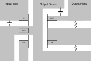
Equivalent series inductance (ESL) and equivalent series resistance (ESR) must be minimized to maximize performance and ensure stability. Every capacitor (CIN, COUT) must be placed as close as possible to the device and on the same side of the PCB as the regulator itself.
Do not place any of the capacitors on the opposite side of the PCB from where the regulator is installed. The use of vias and long traces is strongly discouraged because these circuits may impact system performance negatively, and even cause instability.
11.2 Layout Example
 Figure 24. Recommended Layout
11.3 Power Dissipation and Junction Temperature
Specified regulator operation is assured to a junction temperature of 125°C; the maximum junction temperature allowable to avoid damaging the device is 150°C. This restriction limits the power dissipation the regulator can handle in any given application. To ensure the junction temperature is within acceptable limits, calculate the maximum allowable dissipation, PD(max) and the actual dissipation, PD, which must be less than or equal to PD(max).
The maximum-power-dissipation limit is determined using Equation 3.
where
- TJ(max) is the maximum allowable junction temperature
- RθJA is the thermal resistance junction-to-ambient for the package, see Thermal Information
- TA is the ambient temperature
Use Equation 4 to calculate the regulator dissipation.
Power dissipation resulting from quiescent current is negligible.