SLVSCK0A April 2014 – June 2014 TPS7A8101-Q1
PRODUCTION DATA.
- 1 Features
- 2 Applications
- 3 Description
- 4 Typical Application Circuit
- 5 Revision History
- 6 Pin Configuration and Functions
- 7 Specifications
- 8 Detailed Description
- 9 Application and Implementation
- 10Power Supply Recommendations
- 11Layout
- 12Device and Documentation Support
- 13Mechanical, Packaging, and Orderable Information
パッケージ・オプション
メカニカル・データ(パッケージ|ピン)
- DRB|8
サーマルパッド・メカニカル・データ
- DRB|8
発注情報
8 Detailed Description
8.1 Overview
The TPS7A8101-Q1 device belongs to a family of new-generation LDO regulators that use innovative circuitry to achieve wide bandwidth and high loop gain, resulting in extremely high PSRR (over a 1-MHz range) even with very low headroom (VI – VO). A noise-reduction capacitor (C(NR)) at the NR pin and a bypass capacitor (C(BYPASS)) decrease noise generated by the bandgap reference in order to improve PSRR, while a quick-start circuit fast-charges the noise-reduction capacitor. This family of regulators offers sub-bandgap output voltages, current-limit, and thermal protection, and is fully specified from –40°C to 125°C.
8.2 Functional Block Diagram
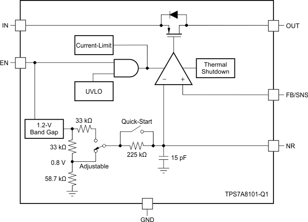 Figure 30. Functional Block Diagram
8.3 Feature Description
8.3.1 Internal Current-Limit
The TPS7A8101-Q1 internal current-limit helps protect the regulator during fault conditions. During the current-limit, the output sources a fixed amount of current that is largely independent of the output voltage. For reliable operation, the device should not be operated in a current-limit state for extended periods of time.
The PMOS pass element in the TPS7A8101-Q1 device has a built-in body diode that conducts current when the voltage at the OUT pin (V(OUT)) exceeds the voltage at the IN pin (V(IN)). This current is not limited, so if extended reverse-voltage operation is anticipated, external limiting may be appropriate.
8.3.2 Shutdown
The enable pin (EN) is active high and is compatible with standard-voltage and low-voltage TTL-CMOS levels. When shutdown capability is not required, the EN pin can connect to the IN pin.
8.3.3 Startup
Through a lower resistance, the bandgap reference can quickly charge the noise-reduction capacitor (C(NR)). The TPS7A8101-Q1 device has a quick-start circuit to quickly charge C(NR), if present; see Figure 30. At startup, this quick-start switch is closed, with only 33 kΩ of resistance between the bandgap reference and the NR pin. The quick-start switch opens approximately 100 ms after any device-enabling event, and the resistance between the bandgap reference and the NR pin becomes higher in value (approximately 250 kΩ) to form a very-good low-pass (RC) filter. This low-pass filter reduces the noise present on the reference voltage; therefore, reducing the noise on the output.
Inrush current can cause problems in many applications. The 33-kΩ resistance during the startup period is intentionally placed between the bandgap reference and the NR pin in order to slow down the reference voltage rampup, thus reducing the inrush current.
Use Equation 1 to calculate the startup time with other C(NR) values. For example, the capacitance of connecting the recommended C(NR) value of 0.47 μF along with the 33-kΩ resistance causes an 80-ms RC delay (approximately).
Although the noise-reduction effect is nearly saturated at 0.47 μF, connecting a C(NR) value greater than 0.47 μF can additionally help reduce noise. However, when connecting a C(NR) value greater than 0.47 µF, the startup time is extremely long because the quick-start switch opens after approximately 100 ms. That is, if C(NR) is not fully charged during this 100-ms period, C(NR) finishes charging through a higher resistance of 250 kΩ, and takes much longer to fully charge.
NOTE
A low-leakage capacitor should be used for C(NR). Most ceramic capacitors are suitable
8.3.4 Undervoltage Lockout (UVLO)
The TPS7A8101-Q1 device uses an undervoltage-lockout (UVLO) circuit to ensure that the output is shut off until the internal circuitry has enough voltage to operate properly. The UVLO circuit has a deglitch feature so that the circuit typically ignores undershoot transients on the input if the duration is less than 50-μs.
8.4 Device Functional Modes
Driving the EN pin over 1.2 V for VI between 2.2 V to 3.6 V or 1.35 V for VI between 3.6 V and 6.5 V turns on the regulator. Driving the EN pin below 0.4 V causes the regulator to enter shutdown mode.
In shutdown, the current consumption of the device is reduced to 0.02 µA typically.