SLVSCK0A April 2014 – June 2014 TPS7A8101-Q1
PRODUCTION DATA.
- 1 Features
- 2 Applications
- 3 Description
- 4 Typical Application Circuit
- 5 Revision History
- 6 Pin Configuration and Functions
- 7 Specifications
- 8 Detailed Description
- 9 Application and Implementation
- 10Power Supply Recommendations
- 11Layout
- 12Device and Documentation Support
- 13Mechanical, Packaging, and Orderable Information
パッケージ・オプション
メカニカル・データ(パッケージ|ピン)
- DRB|8
サーマルパッド・メカニカル・データ
- DRB|8
発注情報
11 Layout
11.1 Layout Guidelines
11.1.1 Board Layout Recommendations To Improve PSRR And Noise Performance
To improve AC performance such as PSRR, output noise, and transient response, designing with separate ground planes for VI and VO, with each ground plane connected only at the GND pin of the device, is recommended. In addition, the ground connection for the noise-reduction capacitor should connect directly to the GND pin of the device.
High ESR capacitors may degrade PSRR.
11.2 Layout Example
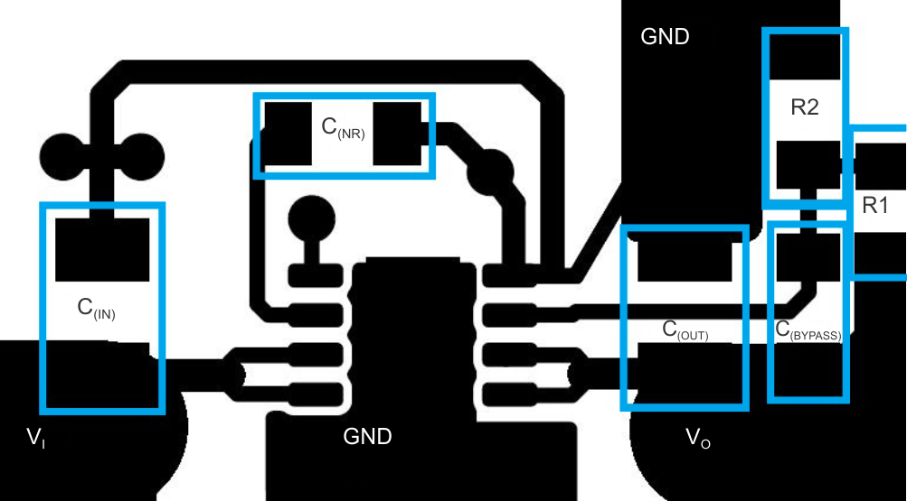 Figure 44. TPS7A8101-Q1 Layout Example
11.3 Thermal Information
11.3.1 Thermal Protection
Thermal protection disables the output when the junction temperature rises to approximately 160°C, allowing the device to cool. When the junction temperature cools to approximately 140°C the output circuitry is again enabled. Depending on power dissipation, thermal resistance, and ambient temperature, the thermal protection circuit may cycle on and off. This cycling limits the dissipation of the regulator, protecting it from damage because of overheating.
Any activation of the thermal protection circuit indicates excessive power dissipation or an inadequate heatsink. For reliable operation, junction temperature should be limited to 125°C (maximum). To estimate the margin of safety in a complete design (including heatsink), increase the ambient temperature until the thermal protection is triggered; use worst-case loads and signal conditions. For good reliability, thermal protection should trigger at least 35°C above the maximum expected ambient condition of your particular application. This configuration produces a worst-case junction temperature of 125°C at the highest expected ambient temperature and worst-case load.
The internal protection circuitry of the TPS7A8101-Q1 device has been designed to protect against overload conditions. The internal thermal protection circuitry was not intended to replace proper heatsinking. Continuously running the TPS7A8101-Q1 device into thermal shutdown degrades device reliability.
11.3.2 Package Mounting
See the Mechanical, Packaging, and Orderable Information section for solder pad footprint recommendations and recommended land patterns.
11.3.3 Power Dissipation
Knowing the device power dissipation and proper sizing of the thermal plane that is connected to the tab or pad is critical to avoiding thermal shutdown and ensuring reliable operation.
The power dissipation of the device depends on input voltage and load conditions. To calculate the device power dissipation, use Equation 3.
Using the lowest possible input voltage necessary to achieve the required output voltage regulation minimizes power dissipation and achieves greater efficiency.
On the SON (DRB) package, the primary conduction path for heat is through the exposed pad to the printed circuit board (PCB). The pad can be connected to ground or can be left floating; however, the pad should be attached to an appropriate amount of copper PCB area to ensure the device does not overheat. The maximum junction-to-ambient thermal resistance depends on the maximum ambient temperature, maximum device junction temperature, and power dissipation of the device. Calculate the maximum junction-to-ambient thermal resistance using Equation 4.
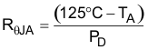
Once the maximum RθJA value is calculated, use Figure 45 to estimate the minimum amount of PCB copper area needed for appropriate heatsinking.
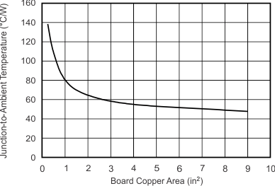
Figure 45 shows the variation of RθJA as a function of ground plane copper area in the board. Figure 45 is intended as a guideline only to demonstrate the effects of heat spreading in the ground plane and should not be used to estimate actual thermal performance in real application environments.
NOTE
When the device is mounted on an application PCB, using ΨJT and ΨJB, as explained in the section is strongly recommended.
11.3.4 Estimating Junction Temperature
Using the thermal metrics ΨJT and ΨJB, as shown in the Thermal Information table, the junction temperature can be estimated with the corresponding equations, Equation 5 and Equation 6. For backwards compatibility, an older θJC,Top parameter is listed as well.
where
- PD is the power dissipation (see Equation 4)
- TT is the temperature at the center-top of the IC package
where
- TB is the PCB temperature measured 1-mm away from the IC package on the PCB surface as shown in Figure 46
 Figure 46. Measuring Points for TT and TB
NOTE
Both TT and TB can be measured on actual application boards using an infrared thermometer.
For more information about measuring TT and TB, see TI's application report SBVA025, Using New Thermal Metrics.
As shown in Figure 47, the new thermal metrics (ΨJT and ΨJB) have very little dependency on board size. That is, using ΨJT or ΨJB with Equation 5 is a good way to estimate TJ by simply measuring TT or TB, regardless of the application board size.
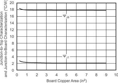 Figure 47. ΨJT and ΨJB vs Board Size
For a more detailed discussion of why TI does not recommend using RθJC(top) to determine thermal characteristics, refer to TI's application report SBVA025, Using New Thermal Metrics. For further information, refer to TI's application report SPRA953, IC Package Thermal Metrics.