JAJSCR3A December 2016 – July 2017 TPSM84A21
PRODUCTION DATA.
- 1 特長
- 2 アプリケーション
- 3 概要
- 4 改訂履歴
- 5 Pin Configuration and Functions
- 6 Specifications
-
7 Detailed Description
- 7.1 Overview
- 7.2 Functional Block Diagram
- 7.3
Feature Description
- 7.3.1 Adjusting the Output Voltage (VADJ)
- 7.3.2 Input and Output Capacitance
- 7.3.3 Transient Response
- 7.3.4 Oscillator Frequency
- 7.3.5 External Clock Syncronization
- 7.3.6 Soft Start
- 7.3.7 Power Good (PGOOD)
- 7.3.8 Gate Driver (VG)
- 7.3.9 Startup into Pre-biased Outputs
- 7.3.10 Thermal Shutdown
- 7.3.11 Overcurrent Protection
- 7.3.12 Output Undervoltage/Overvoltage Protection
- 7.3.13 Enable (EN)
- 7.3.14 Undervoltage Lockout (UVLO)
- 7.4 Device Functional Modes
- 8 Application and Implementation
- 9 Power Supply Recommendations
- 10Layout
- 11デバイスおよびドキュメントのサポート
- 12メカニカル、パッケージ、および注文情報
7 Detailed Description
7.1 Overview
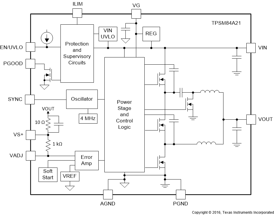
The TPSM84A21 is a 14-V, 10-A, synchronous series capacitor step-down (buck) power module. The TPSM84A21 combines a 10-A DC/DC converter with power MOSFETs, shielded inductors, series capacitor, input and output capacitors, and passives into a low profile, overmolded package. The integrated input and output capacitors allows standard applications to operate with no additional input or output capacitors and only a single resistor to set the output voltage.
The integrated components allow for high-efficiency, high-density, complete power supply designs with continuous output currents up to 10 A. The TPSM84A21 reduces the external component count by integrating both the input and output capacitors. The TPSM84A21 input voltage range is 8 V to 14 V with an output voltage range of 0.508 V to 1.35 V.
The TPSM84A21 is a two-phase power supply with each phase switching at a fixed 2 MHz frequency, resulting in the internal oscillator frequency of 4 MHz. An external synchronization clock can also be provided via the SYNC pin.
The TPSM84A21 starts up safely into loads with pre-biased outputs (non-zero volts at startup). The device implements an internal input voltage under voltage lockout (UVLO) feature which can be adjusted higher by adding an external resistor divider on the EN/UVLO pin. Electrical ON/OFF control is provided using the enable (EN) feature. The TPSM84A21 is disabled by pulling the EN pin low. When the device is disabled, the supply current is typically less than 50 μA.
The TPSM84A21 has a power good comparator (PGOOD) which monitors the output voltage through the VS+ pin. The PGOOD pin is an open-drain MOSFET which is held low until the output voltage is within ±5% of the set voltage. The PGOOD pin is held low during startup or when a fault occurs.
7.2 Functional Block Diagram
7.3 Feature Description
7.3.1 Adjusting the Output Voltage (VADJ)
The VADJ pin programs the output voltage of the TPSM84A21. The output voltage adjustment range is from 0.508 V to 1.35 V. The adjustment method requires the addition of RSET connected between VADJ and AGND. If an RSET resistor is not populated, the module will default to 0.508 V. The VS+ pin (pin 14) must be connected to VOUT. TI recommends to make the VS+ connection at the load for the best load regulation performance. The RSET resistor must be connected directly between the VADJ pin (pin 15) and AGND (pin 16).
Equation 1 can be used to calculate the ideal RSET resistor value for a given output voltage, VOUT. Use Equation 2 to calculate the actual VOUT for a given RSET resistor. Table 1 lists the ideal RSET resistor values for a number of common voltages. Table 1 also lists the closest E96 standard resistor values to the ideal RSET values along with the actual output voltage and the set-point error when using the E96 resistor value. For the most accurate output voltage set-point it is best to use the ideal resistor value. The ideal resistor value may not be a standard value and may require two standard value resistors in series or parallel to obtain the desired output voltage.


Table 1. RSET Resistor Values
| Closest E96 Resistor Value | |||||
|---|---|---|---|---|---|
| VOUT (V) | Ideal RSET (kΩ) | RSET (kΩ) | Actual VOUT (V) | % | |
| 0.508 | Open | Open | 0.508 | – | |
| 0.55 | 12.095 | 12.1 | 0.549 | –0.003 | |
| 0.60 | 5.522 | 5.49 | 0.601 | 0.088 | |
| 0.65 | 3.578 | 3.57 | 0.65 | 0.046 | |
| 0.70 | 2.646 | 2.67 | 0.698 | –0.248 | |
| 0.75 | 2.099 | 2.10 | 0.749 | –0.013 | |
| 0.80 | 1.739 | 1.74 | 0.799 | –0.006 | |
| 0.85 | 1.485 | 1.50 | 0.847 | –0.392 | |
| 0.9 | 1.296 | 1.30 | 0.899 | –0.137 | |
| 0.95 | 1.149 | 1.15 | 0.949 | –0.027 | |
| 1.00 | 1.033 | 1.02 | 1.006 | 0.603 | |
| 1.05 | 0.937 | 0.931 | 1.053 | 0.348 | |
| 1.10 | 0.858 | 0.866 | 1.095 | –0.490 | |
| 1.15 | 0.791 | 0.787 | 1.153 | 0.303 | |
| 1.20 | 0.734 | 0.732 | 1.202 | 0.166 | |
| 1.25 | 0.685 | 0.681 | 1.254 | 0.317 | |
| 1.30 | 0.641 | 0.649 | 1.291 | –0.712 | |
| 1.35 | 0.603 | 0.604 | 1.349 | –0.070 | |
7.3.2 Input and Output Capacitance
The TPSM84A21 requires no external input or output capacitance to operate. Internal to the TPSM84A21 there is 66.1 µF (nominal) of ceramic input capacitance. Additionally, internal to the TPSM84A21 there is 185 µF (nominal) of ceramic output capacitance.
Applications requiring additional ripple voltage reduction should add ceramic input and output capacitors directly at the VIN and VOUT pins of the device. Applications requiring improved transient response can also benefit by adding additonal ceramic or low-ESR bulk output capacitance. See the Capacitance section of the Electrical Characteristics table for more information when adding external input and output capacitors.
7.3.3 Transient Response
The exceptional transient response of the TPSM84A21 allows many applications to operate with little or no additional output capacitance. Figure 11 through Figure 14 show typical transient waveforms for the TPSM84A21.
7.3.3.1 Transient Response Waveforms
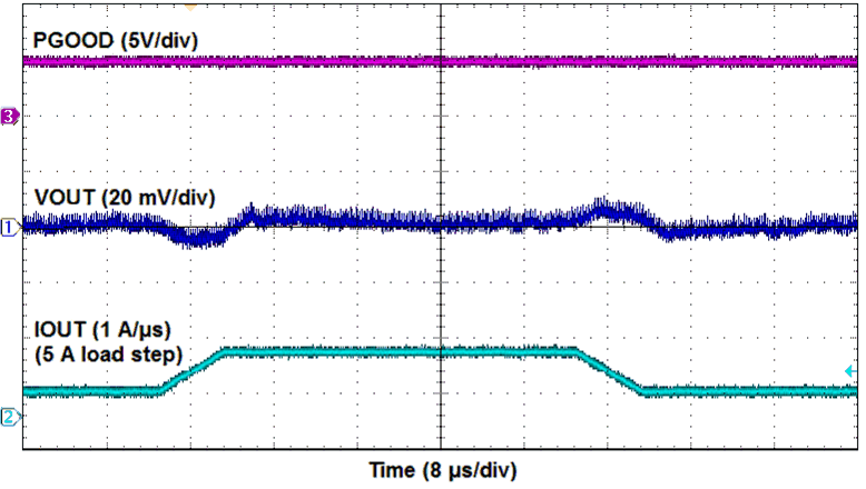
| VIN = 12 V | VOUT = 0.8 V | Load Step = 5 A |
| COUT = 0 µF | Slew Rate = 1 A/µs |
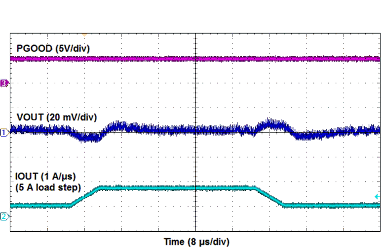
| VIN = 12 V | VOUT = 1.0 V | Load Step = 5 A |
| COUT = 0 µF | Slew Rate = 1 A/µs |
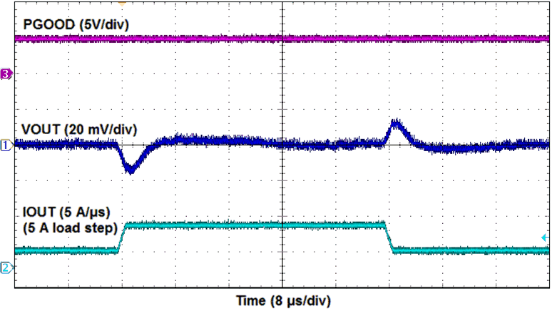
| VIN = 12 V | VOUT = 0.8 V | Load Step = 5 A |
| COUT = 300 µF | Slew Rate = 5 A/µs |
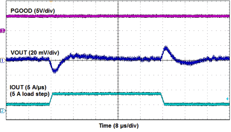
| VIN = 12 V | VOUT = 1.0 V | Load Step = 5 A |
| COUT = 100 µF | Slew Rate = 5 A/µs |
7.3.4 Oscillator Frequency
The oscillator frequency of this converter is set at 4 MHz. The per phase switching frequency of the converter is half the oscillator frequency, or 2 MHz per phase. The oscillator frequency is fixed internally.
During load transients, the internal control loop will momentarily change the switching frequency in order to meet the output voltage recovery.
7.3.5 External Clock Syncronization
An external clock can be connected to the SYNC pin. The external clock signal overrides the internal oscillator and is used as the system clock. This feature enables the user to synchronize the switching events to a master clock on their board. The internal phase locked loop (PLL) has been implemented to allow synchronization at frequencies between ±10% of the nominal oscillator frequency. This allows the user to easily switch between the internal oscillator mode and the external clock mode while converting power. Before the external clock is present or after it is removed, the device with default to the internal oscillator setting.
To implement the synchronization feature, connect a square wave clock signal to the SYNC pin with a duty cycle between 20% and 80%. The clock signal amplitude must transition lower than 0.8 V and higher than 2 V. The start of the switching cycle is synchronized to the rising edge of the SYNC pin. The device can be configured for operation in applications where both an internal oscillator mode and an external synchronization clock mode are needed. Before the external clock is present, the switching frequency of the device is set by the internal oscillator. When the external clock is present, the SYNC mode overrides the internal oscillator. The first time the SYNC pin is pulled above the SYNC high threshold (2 V), the device switches from the internal oscillator mode to the SYNC mode and the PLL starts to lock onto the frequency of the external clock. When the external SYNC clock is removed, the converter will transition back to the internal oscillator after 4 internal clock cycles.
7.3.6 Soft Start
The TPSM84A21 has a pre-programmed soft start time of 4.1 ms (typ). The soft start time is the time it takes for the output voltage to rise from zero volts to the voltage set by the RSET resistor. Soft start is an important feature that limits inrush current and reduces the load on the input supply to this device. During soft start, the internal reference voltage is slowly ramped up to the internal reference voltage. This slowly increases the commanded output voltage of the converter and reduces the initial surge in current. During soft start PGOOD remains low, the PLL is not active, and output UVP/OVP faults are disabled.
7.3.7 Power Good (PGOOD)
The Power Good (PGOOD) pin is an open drain output. After startup, when the VADJ pin is typically between 95% and 105% of the internal voltage reference, the PGOOD pin pull-down is released and the pin floats. The recommended pull-up resistor value is between 10 kΩ and 100 kΩ to a voltage source of 5.5 V or less. For convenience, VG can be used as the pull-up voltage. The PGOOD is in a defined state once the VIN input voltage is greater than approximately 1.2 V, but with reduced current sinking capability. The PGOOD achieves full current sinking capability once the VIN input voltage is above the input UVLO. The PGOOD pin is pulled low when the VADJ pin voltage is typically lower than 95% or greater than 105% of the nominal internal reference voltage. The PGOOD pin is also pulled low if a fault is detected, the EN pin is pulled low, or the converter is performing its soft-start power up sequence.
7.3.8 Gate Driver (VG)
A linear regulator internal to the TPSM84A21 generates a 4.8 V internal supply rail on the VG pin. The input of the linear regulator comes from the VIN pin. The VG supply rail is used to power the internal gate drivers and is the input to another regulator that generates the internal supply rails used by the controller. To improve converter efficiency, an external 5 V supply is recommended to be connected to the VG pin, thereby overriding the internal 4.8 V regulator. This external supply must be between 5.0 V and 5.5 V and must be present before applying input voltage to the VIN pin. If not supplying an external voltage to this pin, leave this pin open.
7.3.9 Startup into Pre-biased Outputs
The TPSM84A21 prevents the low-side MOSFETs from discharging a pre-biased output. During pre-biased startup, the low-side MOSFETs do not turn on until after the high-side MOSFETs have started switching. The high-side MOSFETs do not start switching until the internal soft-start reference voltage exceeds the voltage at the VADJ pin.
7.3.10 Thermal Shutdown
The internal thermal shutdown fault is triggered if the junction temperature exceeds 135°C (typ). This interrupts regulation by making the output high impedance. The device reinitiates the power up sequence when the junction temperature drops below 115°C (typ).
7.3.11 Overcurrent Protection
For protection against load faults, the TPSM84A21 incorporates output overcurrent protection. Applying a load that exceeds the module's overcurrent threshold causes the output to shut down and PGOOD is pulled low. Following shut down, the module attempts to restart after a 32.8-ms hiccup interval counter has expired. This provides a hiccup response to an overcurrent condition. During this period, the average current flowing into the fault is significantly reduced which reduces power dissipation. Once the fault is removed, the module automatically recovers and returns to normal operation.
The TPSM84A21 overcurrent trip point is 15 A (typ) when the ILIM pin is left open. This provides enough margin for brief overshoots in inductor currents during a load transient while at the same time protecting against short circuits or other potentially catastrophic faults on the output. The overcurrent trip point can be reduced to 11.25 A (typ) by placing a 47 kΩ between the ILIM pin and PGND. Programming resistors with up to ±5% variation can be used. The current limit selection is latched in at power up and cannot be changed without cycling input power or the EN pin voltage.
7.3.12 Output Undervoltage/Overvoltage Protection
The device incorporates an output undervoltage/overvoltage protection (UVP/OVP) circuit to prevent damage to the load. This fault can be triggered during large, fast load transients if insufficient output capacitance is used. The UVP/OVP feature compares the VADJ pin voltage to internal thresholds. If the VADJ pin voltage is lower than 90% or greater than 110% of the nominal internal reference voltage, the module is turned off, a fault is triggered, and the PGOOD pin is pulled low. When the fault hiccup interval is complete, the module will attempt to restart.
7.3.13 Enable (EN)
The EN pin provides electrical on and off control of the TPSM84A21. Once the EN pin voltage exceeds the threshold voltage, the device starts operation. If the EN pin voltage is pulled below the threshold voltage, the module stops switching and enters a low power state. There is no voltage hysteresis in the EN threshold. The rising and falling voltage thresholds occur at the same level. The EN pin has an internal pull-up current source, allowing the user to float the EN pin for enabling the device.
If an application requires controlling the EN pin, use an open drain/collector device or a suitable logic gate to interface with the pin. Figure 15 shows controlling the EN/UVLO pin using a MOSFET, Q1. Turning Q1 on, disables the device. Using a voltage superviser to control the EN pin allows control of the turn-on and turn-off of the device as opposed to relying on the ramp up or down of the input voltage source.
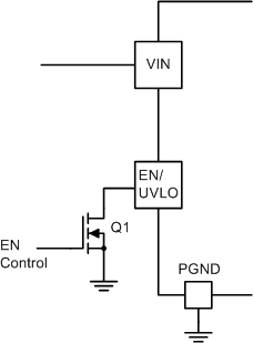 Figure 15. Enable Control
7.3.14 Undervoltage Lockout (UVLO)
The TPSM84A21 implements internal UVLO circuitry on the VIN pin. The device is disabled when the VIN pin voltage is below the internal VIN UVLO threshold. The internal VIN UVLO rising threshold is 7.65 V(max) with a typical hysteresis of 250 mV.
If an application requires a higher UVLO threshold, the UVLO pin can be configured as shown in Figure 16. The value of RUVLO1 and RUVLO2 can be calculated using Equation 3 and Equation 4 or selected from Table 2. It is recommended to set the UVLO hysteresis of approximately 500mV in order to avoid repeated chatter during start up or shut down. Table 2 shows recommended RUVLO1 and RUVLO2 values for various VIN UVLO rising thresholds, with 500 mV of hysteresis.


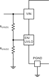 Figure 16. Adjustable UVLO
Table 2. Standard Resistor Values For Adjusting VIN UVLO
| VIN UVLO RISING THRESHOLD (V) | 8.0 | 8.5 | 9.0 | 9.5 | 10.0 |
|---|---|---|---|---|---|
| VIN UVLO FALLING THRESHOLD (V) | 7.5 | 8.0 | 8.5 | 9.0 | 9.5 |
| RUVLO1 (kΩ) | 169 | 169 | 169 | 169 | 169 |
| RUVLO2 (kΩ) | 29.4 | 27.4 | 25.5 | 24.3 | 22.6 |
7.4 Device Functional Modes
7.4.1 Active Mode
The TPSM84A21 is in Active Mode when VIN is above the UVLO threshold and the EN/UVLO pin voltage is above the EN high threshold. The simplest way to enable the TPSM84A21 is to leave the EN/UVLO pin floating. This allows self start-up of the TPSM84A21 when the input voltage is above the UVLO threshold.
7.4.2 Light Load Operation
The TPSM84A21 operates in forced continuous conduction mode (FCCM) under light load conditions. When operating in FCCM, the switching frequency remains constant and the high side and low side MOSFETs are turned on and off in a complementary fashion allowing negative inductor current for part of the switching cycle.
7.4.3 Shutdown Mode
The EN/UVLO pin provides electrical ON and OFF control for the TPSM84A21. When the EN/UVLO pin voltage is below the EN threshold, the device is in shutdown mode. In shutdown mode the stand-by current is typically less than 50 μA. The TPSM84A21 also employs under voltage lock out protection. If VIN is below the UVLO level, the output of the regulator turns off.