JAJSGJ8C November 2018 – September 2019 UCC20225-Q1 , UCC20225A-Q1
PRODUCTION DATA.
- 1 特長
- 2 アプリケーション
- 3 概要
- 4 改訂履歴
- 5 概要(続き)
- 6 Pin Configuration and Functions
-
7 Specifications
- 7.1 Absolute Maximum Ratings
- 7.2 ESD Ratings
- 7.3 Recommended Operating Conditions
- 7.4 Thermal Information
- 7.5 Power Ratings
- 7.6 Insulation Specifications
- 7.7 Safety-Related Certifications
- 7.8 Safety Limiting Values
- 7.9 Electrical Characteristics
- 7.10 Switching Characteristics
- 7.11 Thermal Derating Curves
- 7.12 Typical Characteristics
- 8 Parameter Measurement Information
- 9 Detailed Description
-
10Application and Implementation
- 10.1 Application Information
- 10.2
Typical Application
- 10.2.1 Design Requirements
- 10.2.2
Detailed Design Procedure
- 10.2.2.1 Designing PWM Input Filter
- 10.2.2.2 Select External Bootstrap Diode and its Series Resistor
- 10.2.2.3 Gate Driver Output Resistor
- 10.2.2.4 Estimate Gate Driver Power Loss
- 10.2.2.5 Estimating Junction Temperature
- 10.2.2.6 Selecting VCCI, VDDA/B Capacitor
- 10.2.2.7 Dead Time Setting Guidelines
- 10.2.2.8 Application Circuits with Output Stage Negative Bias
- 10.2.3 Application Curves
- 11Power Supply Recommendations
- 12Layout
- 13デバイスおよびドキュメントのサポート
- 14メカニカル、パッケージ、および注文情報
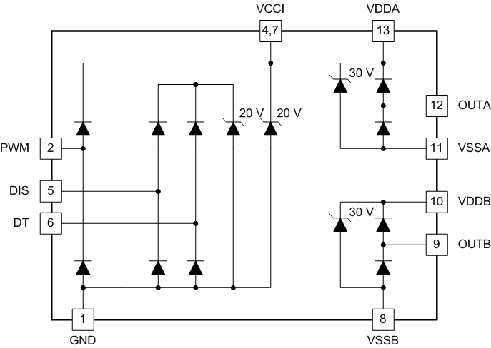
9.3.5 Diode Structure in UCC20225-Q1 family
Figure 35 illustrates the multiple diodes involved in the ESD protection components of the UCC20225-Q1 family. This provides a pictorial representation of the absolute maximum rating for the device.
 Figure 35. ESD Structure