JAJSGJ8C November 2018 – September 2019 UCC20225-Q1 , UCC20225A-Q1
PRODUCTION DATA.
- 1 特長
- 2 アプリケーション
- 3 概要
- 4 改訂履歴
- 5 概要(続き)
- 6 Pin Configuration and Functions
-
7 Specifications
- 7.1 Absolute Maximum Ratings
- 7.2 ESD Ratings
- 7.3 Recommended Operating Conditions
- 7.4 Thermal Information
- 7.5 Power Ratings
- 7.6 Insulation Specifications
- 7.7 Safety-Related Certifications
- 7.8 Safety Limiting Values
- 7.9 Electrical Characteristics
- 7.10 Switching Characteristics
- 7.11 Thermal Derating Curves
- 7.12 Typical Characteristics
- 8 Parameter Measurement Information
- 9 Detailed Description
-
10Application and Implementation
- 10.1 Application Information
- 10.2
Typical Application
- 10.2.1 Design Requirements
- 10.2.2
Detailed Design Procedure
- 10.2.2.1 Designing PWM Input Filter
- 10.2.2.2 Select External Bootstrap Diode and its Series Resistor
- 10.2.2.3 Gate Driver Output Resistor
- 10.2.2.4 Estimate Gate Driver Power Loss
- 10.2.2.5 Estimating Junction Temperature
- 10.2.2.6 Selecting VCCI, VDDA/B Capacitor
- 10.2.2.7 Dead Time Setting Guidelines
- 10.2.2.8 Application Circuits with Output Stage Negative Bias
- 10.2.3 Application Curves
- 11Power Supply Recommendations
- 12Layout
- 13デバイスおよびドキュメントのサポート
- 14メカニカル、パッケージ、および注文情報
10.2.3 Application Curves
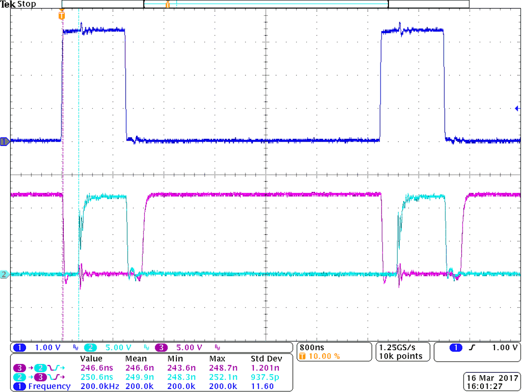
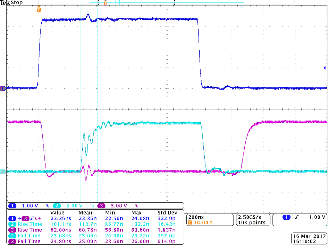
Figure 41 and Figure 42 shows the bench test waveforms for the design example shown in Figure 37 under these conditions: VCC = 5 V, VDD = 12 V, fSW = 200 kHz, VDC-Link = 400 V.
Channel 1 (Indigo): UCC20225-Q1 family's PWM pin signal.
Channel 2 (Cyan): Gate-source signal on the high side power transistor.
Channel 3 (Magenta): Gate-source signal on the low side power transistor.
In Figure 41, PWM is sent a 3.3 V, 20% duty-cycle signal. The gate drive signals on the power transistor have a 250-ns dead time, shown in the measurement section of Figure 41. The dead time matching is 10-ns with the 250-ns dead time setting. Note that with high voltage present, lower bandwidth differential probes are required, which limits the achievable accuracy of the measurement.
Figure 42 shows a zoomed-in version of the waveform of Figure 41, with measurements for propagation delay and rising/falling time. Importantly, the output waveform is measured between the power transistors’ gate and source pins, and is not measured directly from the driver OUTA and OUTB pins. Due to the split on and off resistors (RON, ROFF), different sink and source currents, and the Miller plateau, different rising (60, 120 ns) and falling time (25 ns) are observed in Figure 42.

