SLUSBP4B August 2013 – October 2014 UCC27524A
PRODUCTION DATA.
- 1 Features
- 2 Applications
- 3 Description
- 4 Revision History
- 5 Description (Continued)
- 6 Pin Configuration and Functions
- 7 Specifications
- 8 Detailed Description
- 9 Applications and Implementation
- 10Power Supply Recommendations
- 11Layout
- 12Device and Documentation Support
- 13Mechanical, Packaging, and Orderable Information
パッケージ・オプション
メカニカル・データ(パッケージ|ピン)
サーマルパッド・メカニカル・データ
- DGN|8
発注情報
7 Specifications
7.1 Absolute Maximum Ratings(1)(2)
over operating free-air temperature range (unless otherwise noted)| MIN | MAX | UNIT | ||
|---|---|---|---|---|
| Supply voltage range | VDD | –0.3 | 20 | V |
| OUTA, OUTB voltage | DC | –0.3 | VDD + 0.3 | V |
| Repetitive pulse < 200 ns(4) | –2 | VDD + 0.3 | V | |
| Output continuous source/sink current | IOUT_DC | 0.3 | A | |
| Output pulsed source/sink current (0.5 µs) | IOUT_pulsed | 5 | A | |
| INA, INB, ENA, ENB voltage(3) | –5 | 20 | V | |
| Operating virtual junction temperature, TJ range | –40 | 150 | °C | |
| Lead temperature | Soldering, 10 seconds | 300 | °C | |
| Reflow | 260 | °C | ||
(1) Stresses beyond those listed under Absolute Maximum Ratings may cause permanent damage to the device. These are stress ratings only and functional operation of the device at these or any other conditions beyond those indicated under Recommended Operating Conditions is not implied. Exposure to absolute-maximum-rated conditions for extended periods may affect device reliability.
(2) All voltages are with respect to GND unless otherwise noted. Currents are positive into, negative out of the specified terminal. See Packaging Section of the datasheet for thermal limitations and considerations of packages.
(3) The maximum voltage on the Input and Enable pins is not restricted by the voltage on the VDD pin.
(4) Values are verified by characterization on bench.
7.2 Handling Ratings
| MIN | MAX | UNIT | |||
|---|---|---|---|---|---|
| Tstg | Storage temperature range | –65 | 150 | °C | |
| V(ESD) | Electrostatic discharge | Human body model (HBM), per ANSI/ESDA/JEDEC JS-001, all pins(1) | –4000 | 4000 | V |
| Charged device model (CDM), per JEDEC specification JESD22-C101, all pins(2) | –1000 | 1000 | |||
(1) JEDEC document JEP155 states that 500-V HBM allows safe manufacturing with a standard ESD control process.
(2) JEDEC document JEP157 states that 250-V CDM allows safe manufacturing with a standard ESD control process.
7.3 Recommended Operating Conditions
over operating free-air temperature range (unless otherwise noted)| MIN | TYP | MAX | UNIT | |
|---|---|---|---|---|
| Supply voltage range, VDD | 4.5 | 12 | 18 | V |
| Operating junction temperature range | –40 | 140 | °C | |
| Input voltage, INA, INB | –2 | 18 | V | |
| Enable voltage, ENA and ENB | –2 | 18 |
7.4 Thermal Information
| THERMAL METRIC | UCC27524A | UCC27524A | UNIT | |
|---|---|---|---|---|
| SOIC (D) | MSOP (DGN)(1) | |||
| 8 PINS | 8 PINS | |||
| θJA | Junction-to-ambient thermal resistance(2) | 130.9 | 71.8 | °C/W |
| θJCtop | Junction-to-case (top) thermal resistance(3) | 80.0 | 65.6 | |
| θJB | Junction-to-board thermal resistance(4) | 71.4 | 7.4 | |
| ψJT | Junction-to-top characterization parameter(5) | 21.9 | 7.4 | |
| ψJB | Junction-to-board characterization parameter(6) | 70.9 | 31.5 | |
| θJCbot | Junction-to-case (bottom) thermal resistance(7) | n/a | 19.6 | |
(1) For more information about traditional and new thermal metrics, see the IC Package Thermal Metrics application report, SPRA953.
(2) The junction-to-ambient thermal resistance under natural convection is obtained in a simulation on a JEDEC-standard, high-K board, as specified in JESD51-7, in an environment described in JESD51-2a.
(3) The junction-to-case (top) thermal resistance is obtained by simulating a cold plate test on the package top. No specific JEDEC-standard test exists, but a close description can be found in the ANSI SEMI standard G30-88.
(4) The junction-to-board thermal resistance is obtained by simulating in an environment with a ring cold plate fixture to control the PCB temperature, as described in JESD51-8.
(5) The junction-to-top characterization parameter, ψJT, estimates the junction temperature of a device in a real system and is extracted from the simulation data for obtaining θJA, using a procedure described in JESD51-2a (sections 6 and 7).
(6) The junction-to-board characterization parameter, ψJB, estimates the junction temperature of a device in a real system and is extracted from the simulation data for obtaining θJA , using a procedure described in JESD51-2a (sections 6 and 7).
(7) The junction-to-case (bottom) thermal resistance is obtained by simulating a cold plate test on the exposed (power) pad. No specific JEDEC standard test exists, but a close description can be found in the ANSI SEMI standard G30-88.
7.5 Electrical Characteristics
VDD = 12 V, TA = TJ = –40 °C to 140 °C, 1-µF capacitor from VDD to GND. Currents are positive into, negative out of the specified terminal (unless otherwise noted,)| PARAMETER | TEST CONDITION | MIN | TYP | MAX | UNIT | |
|---|---|---|---|---|---|---|
| BIAS CURRENTS | ||||||
| IDD(off) | Startup current, (based on UCC27524 Input configuration) |
VDD = 3.4 V, INA = VDD, INB = VDD |
55 | 110 | 175 | μA |
| VDD = 3.4 V, INA = GND, INB = GND |
25 | 75 | 145 | |||
| UNDER VOLTAGE LOCKOUT (UVLO) | ||||||
| VON | Supply start threshold | TJ = 25 °C | 3.91 | 4.2 | 4.5 | V |
| TJ = –40 °C to 140 °C | 3.7 | 4.2 | 4.65 | |||
| VOFF | Minimum operating voltage after supply start | 3.4 | 3.9 | 4.4 | ||
| VDD_H | Supply voltage hysteresis | 0.2 | 0.3 | 0.5 | ||
| INPUTS (INA, INB, INA+, INA–, INB+, INB–), UCC27524A (D, DGN) | ||||||
| VIN_H | Input signal high threshold | Output high for non-inverting input pins Output low for inverting input pins |
1.9 | 2.1 | 2.3 | V |
| VIN_L | Input signal low threshold | Output low for non-inverting input pins Output high for inverting input pins |
1 | 1.2 | 1.4 | |
| VIN_HYS | Input hysteresis | 0.7 | 0.9 | 1.1 | ||
| OUTPUTS (OUTA, OUTB) | ||||||
| ISNK/SRC | Sink/source peak current(1) | CLOAD = 0.22 µF, FSW = 1 kHz | ±5 | A | ||
| VDD-VOH | High output voltage | IOUT = –10 mA | 0.075 | V | ||
| VOL | Low output voltage | IOUT = 10 mA | 0.01 | |||
| ROH | Output pullup resistance(2) | IOUT = –10 mA | 2.5 | 5 | 7.5 | Ω |
| ROL | Output pulldown resistance | IOUT = 10 mA | 0.15 | 0.5 | 1 | Ω |
(1) Ensured by design.
(2) ROH represents on-resistance of only the P-Channel MOSFET device in the pullup structure of the UCC27524A output stage.
7.6 Switching Characteristics
over operating free-air temperature range (unless otherwise noted)| PARAMETER | TEST CONDITIONS | MIN | TYP | MAX | UNIT | |
|---|---|---|---|---|---|---|
| tR | Rise time(1) | CLOAD = 1.8 nF | 7 | 18 | ns | |
| tF | Fall time(1) | CLOAD = 1.8 nF | 6 | 10 | ||
| tM | Delay matching between 2 channels | INA = INB, OUTA and OUTB at 50% transition point | 1 | 4 | ||
| tPW | Minimum input pulse width that changes the output state | 15 | 25 | |||
| tD1, tD2 | Input to output propagation delay(1) | CLOAD = 1.8 nF, 5-V input pulse | 6 | 13 | 23 | |
| tD3, tD4 | EN to output propagation delay(1) | CLOAD = 1.8 nF, 5-V enable pulse | 6 | 13 | 23 | |
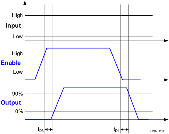 Figure 1. Enable Function
 (For Non-Inverting Input-Driver Operation)
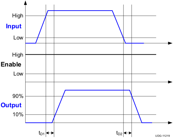 Figure 2. Non-Inverting Input-Driver Operation
7.7 Typical Characteristics
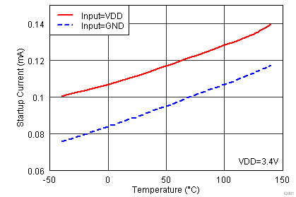 Figure 3. Start-Up Current vs Temperature
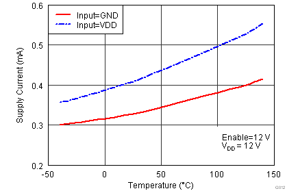 Figure 5. Supply Current vs Temperature (Outputs In DC On/Off Condition)
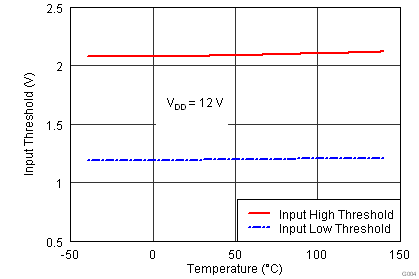 Figure 7. Input Threshold vs Temperature
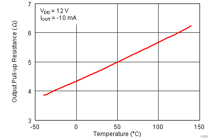 Figure 9. Output Pullup Resistance vs Temperature
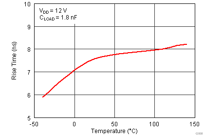 Figure 11. Rise Time vs Temperature
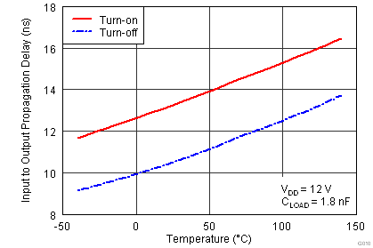 Figure 13. Input to Output Propagation Delay vs Temperature
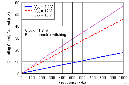 Figure 15. Operating Supply Current vs Frequency
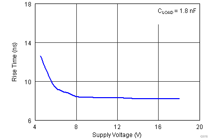 Figure 17. Rise Time vs Supply Voltage
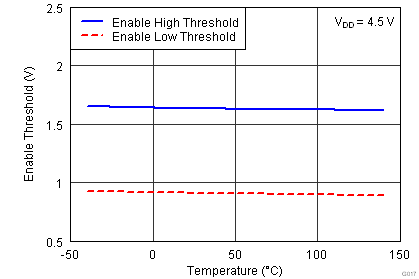 Figure 19. Enable Threshold vs Temperature
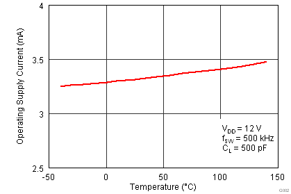 Figure 4. Operating Supply Current vs Temperature (Outputs Switching)
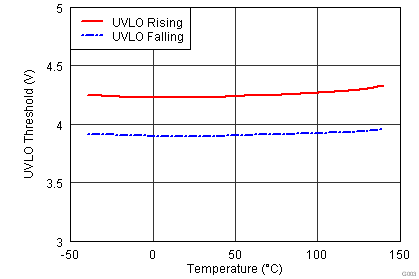 Figure 6. UVLO Threshold vs Temperature
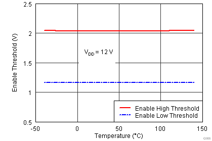 Figure 8. Enable Threshold vs Temperature
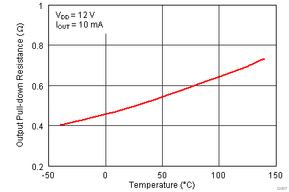 Figure 10. Output Pulldown Resistance vs Temperature
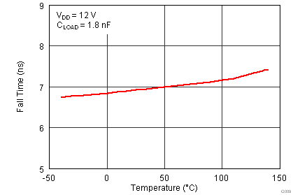 Figure 12. Fall Time vs Temperature
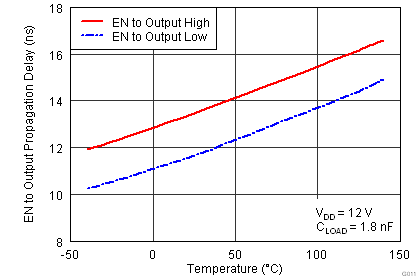 Figure 14. En to Output Propagation Delay vs Temperature
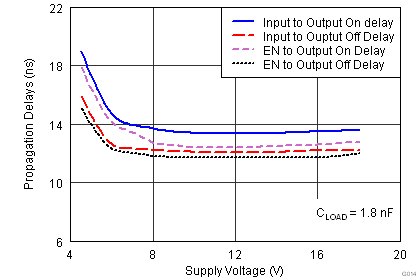 Figure 16. Propagation Delays vs Supply Voltage
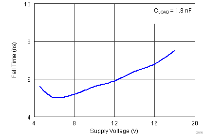 Figure 18. Fall Time vs Supply Voltage