JAJSDC3A June   2017  – August 2018 UCC27712

PRODUCTION DATA.  

  1. 特長
  2. アプリケーション
  3. 概要
    1.     Device Images
      1.      概略回路図
      2.      標準的な伝播遅延の比較
  4. 改訂履歴
  5. 概要(続き)
  6. Pin Configuration and Functions
    1.     Pin Functions
  7. Specifications
    1. 7.1 Absolute Maximum Ratings
    2. 7.2 ESD Ratings
    3. 7.3 Recommended Operating Conditions
    4. 7.4 Thermal Information
    5. 7.5 Electrical Characteristics
    6. 7.6 Dynamic Electrical Characteristics
    7. 7.7 Typical Characteristics
  8. Detailed Description
    1. 8.1 Overview
    2. 8.2 Functional Block Diagram
    3. 8.3 Feature Description
      1. 8.3.1 VDD and Under Voltage Lockout
      2. 8.3.2 Input and Output Logic Table
      3. 8.3.3 Input Stage
      4. 8.3.4 Output Stage
      5. 8.3.5 Level Shift
      6. 8.3.6 Low Propagation Delays and Tightly Matched Outputs
      7. 8.3.7 Parasitic Diode Structure
    4. 8.4 Device Functional Modes
      1. 8.4.1 Minimum Input Pulse Operation
      2. 8.4.2 Output Interlock and Dead Time
      3. 8.4.3 Operation Under 100% Duty Cycle Condition
      4. 8.4.4 Operation Under Negative HS Voltage Condition
  9. Application and Implementation
    1. 9.1 Application Information
    2. 9.2 Typical Application
      1. 9.2.1 Design Requirements
      2. 9.2.2 Detailed Design Procedure
        1. 9.2.2.1 Selecting HI and LI Low Pass Filter Components (RHI, RLI, CHI, CLI)
        2. 9.2.2.2 Selecting Bootstrap Capacitor (CBOOT)
        3. 9.2.2.3 Selecting VDD Bypass/Holdup Capacitor (CVDD) and Rbias
        4. 9.2.2.4 Selecting Bootstrap Resistor (RBOOT)
        5. 9.2.2.5 Selecting Gate Resistor RON/ROFF
        6. 9.2.2.6 Selecting Bootstrap Diode
        7. 9.2.2.7 Estimate the UCC27712 Power Losses (PUCC27712)
        8. 9.2.2.8 Estimating Junction Temperature
        9. 9.2.2.9 Operation With IGBT's
      3. 9.2.3 Application Curves
  10. 10Power Supply Recommendations
  11. 11Layout
    1. 11.1 Layout Guidelines
    2. 11.2 Layout Example
  12. 12デバイスおよびドキュメントのサポート
    1. 12.1 ドキュメントのサポート
      1. 12.1.1 関連資料
    2. 12.2 関連リンク
    3. 12.3 コミュニティ・リソース
    4. 12.4 商標
    5. 12.5 静電気放電に関する注意事項
    6. 12.6 Glossary
  13. 13メカニカル、パッケージ、および注文情報

パッケージ・オプション

メカニカル・データ(パッケージ|ピン)
サーマルパッド・メカニカル・データ
発注情報

Typical Characteristics
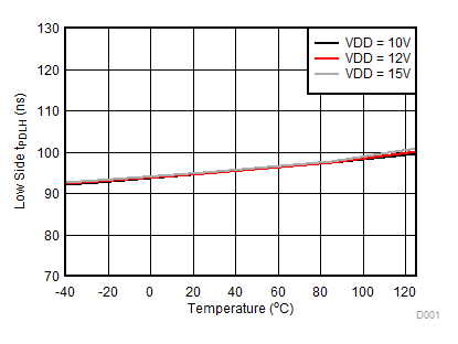
UCC27712 D001_slusce9.gif
Figure 2. Low-Side, Turn-On Propagation Delay vs Temperature
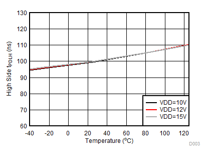
UCC27712 D003_slusce9.gif
Figure 4. High-Side, Turn-On Propagation Delay vs Temperature
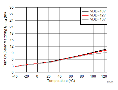
UCC27712 D005_slusce9.gif
Figure 6. Turn-On Delay Matching vs Temperature
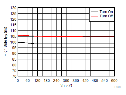
UCC27712 d007new_slusce9.gif
Figure 8. High-Side Propagation Delay vs HS
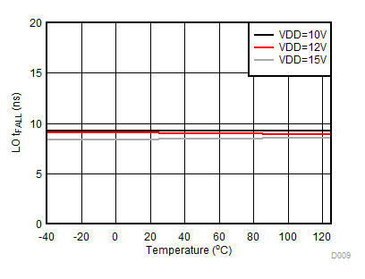
UCC27712 D009_slusce9.gif
Figure 10. LO Fall Time with 1000-pF Load vs Temperature
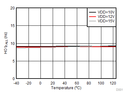
UCC27712 D0011_slusce9.gif
Figure 12. HO Fall Time with 1000-pF Load vs Temperature
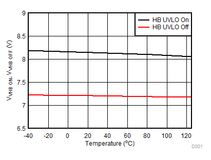
UCC27712 D0013_slusce9.gif
Figure 14. VHB-VHS UVLO Thresholds vs Temperature
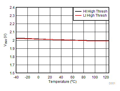
UCC27712 D0015_slusce9.gif
Figure 16. HI/LI Pin High Threshold vs Temperature
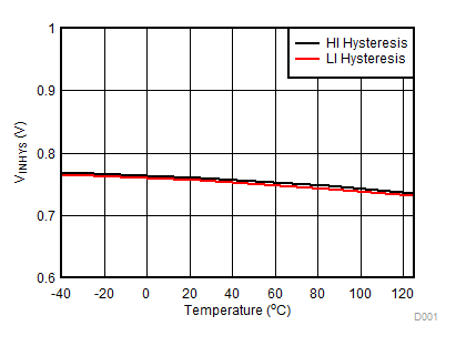
UCC27712 D0017_slusce9.gif
Figure 18. HI/LI Pin Hysteresis vs Temperature
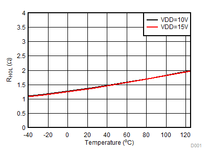
UCC27712 D0019_slusce9.gif
Figure 20. HO Output Pull-Down Resistance vs Temperature
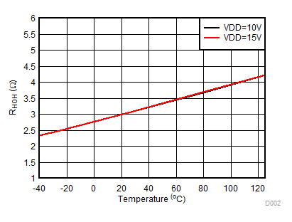
UCC27712 D0021_slusce9.gif
Figure 22. HO Output Pull-Up Resistance vs Temperature
UCC27712 D0023_slusce9.gif
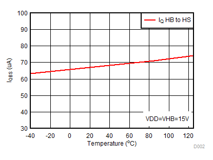
Figure 24. Quiescent HB to HS Supply Current vs Temperature
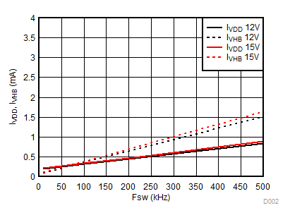
UCC27712 D0025_slusce9.gif
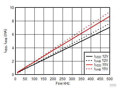
Figure 26. VDD and HB Operating Current with No Load vs Switching Frequency
UCC27712 D0027_slusce9.gif
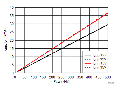
Figure 28. VDD and HB Operating Current with 4700-pF Load vs Switching Frequency
UCC27712 D002_slusce9.gif
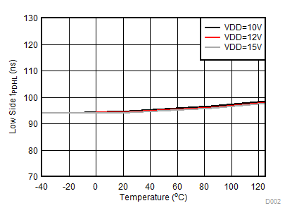
Figure 3. Low-Side, Turn-Off Propagation Delay vs Temperature
UCC27712 D004_slusce9.gif
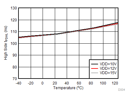
Figure 5. High-Side, Turn-Off Propagation Delay vs Temperature
UCC27712 D006_slusce9.gif
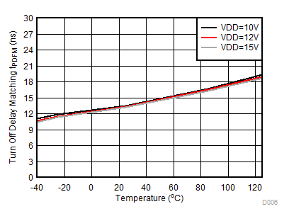
Figure 7. Turn-Off Delay Matching vs Temperature
UCC27712 D008_slusce9.gif
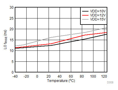
Figure 9. LO Rise Time with 1000-pF Load vs Temperature
UCC27712 D0010_slusce9.gif
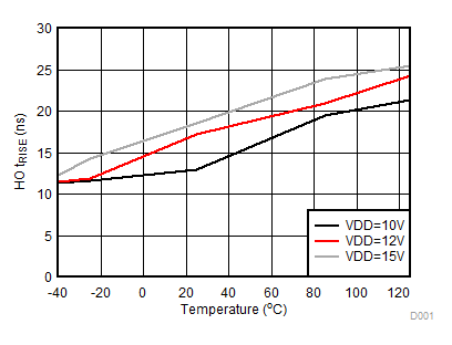
Figure 11. HO Rise Time with 1000-pF Load vs Temperature
UCC27712 D0012_slusce9.gif
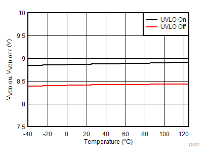
Figure 13. VDD UVLO Thresholds vs Temperature
UCC27712 D0014_slusce9.gif
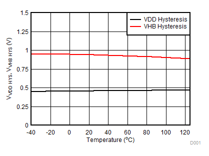
Figure 15. VDD and VHB-VHS UVLO Hysteresis vs Temperature
UCC27712 D0016_slusce9.gif
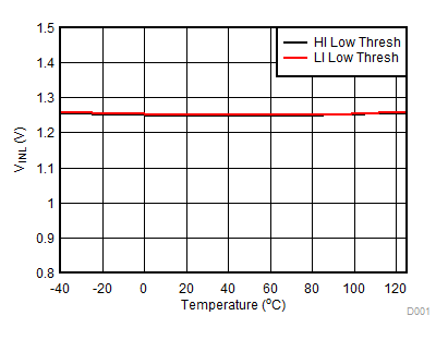
Figure 17. HI/LI Pin Low Threshold vs Temperature
UCC27712 D0018_slusce9.gif
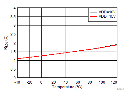
Figure 19. LO Output Pull-Down Resistance vs Temperature
UCC27712 D0020_slusce9.gif
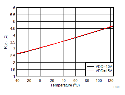
Figure 21. LO Output Pull-Up Resistance vs Temperature
UCC27712 D0022_slusce9.gif
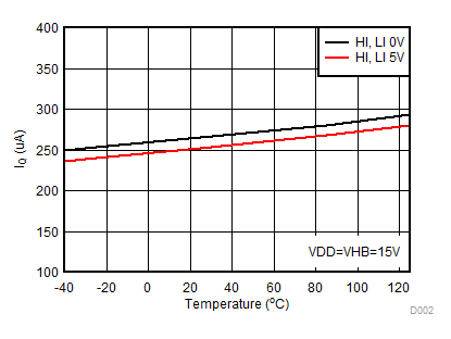
Figure 23. Total Quiescent VDD plus HB Supply Current vs Temperature
UCC27712 D0024_slusce9.gif
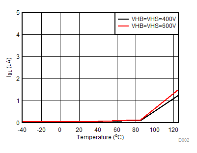
Figure 25. HB to COM Bootstrap Supply Leakage Current vs Temperature
UCC27712 D0026_slusce9.gif
Figure 27. VDD and HB Operating Current with 1000-pF Load vs Switching Frequency