SLUSAO7B September 2011 – November 2016 UCC28063
PRODUCTION DATA.
- 1 Features
- 2 Applications
- 3 Description
- 4 Revision History
- 5 Description (Continued)
- 6 Pin Configuration and Functions
- 7 Specifications
-
8 Detailed Description
- 8.1 Overview
- 8.2 Functional Block Diagram
- 8.3
Feature Description
- 8.3.1 Principles of Operation
- 8.3.2 Natural Interleaving
- 8.3.3 On-Time Control, Maximum Frequency Limiting, and Restart Timer
- 8.3.4 Distortion Reduction
- 8.3.5 Zero-Current Detection and Valley Switching
- 8.3.6 Phase Management and Light-Load Operation
- 8.3.7 External Disable
- 8.3.8 Improved Error Amplifier
- 8.3.9 Soft Start
- 8.3.10 Brownout Protection
- 8.3.11 Dropout Detection
- 8.3.12 VREF
- 8.3.13 VCC
- 8.3.14 Control of Downstream Converter
- 8.3.15
System Level Protections
- 8.3.15.1 Failsafe OVP - Output Overvoltage Protection
- 8.3.15.2 Overcurrent Protection
- 8.3.15.3 Open-Loop Protection
- 8.3.15.4 VCC Undervoltage Lock-Out (UVLO) Protection
- 8.3.15.5 Phase-Fail Protection
- 8.3.15.6 CS-Open, TSET-Open and -Short Protection
- 8.3.15.7 Thermal Shutdown Protection
- 8.3.15.8 AC-Line Brownout and Dropout Protections
- 8.3.15.9 Fault Logic Diagram
- 8.4 Device Functional Modes
-
9 Applications and Implementation
- 9.1 Application Information
- 9.2
Typical Application
- 9.2.1 Design Requirements
- 9.2.2
Detailed Design Procedure
- 9.2.2.1 Inductor Selection
- 9.2.2.2 ZCD Resistor Selection (RZA, RZB)
- 9.2.2.3 HVSEN
- 9.2.2.4 Output Capacitor Selection
- 9.2.2.5 Selecting (RS) For Peak Current Limiting
- 9.2.2.6 Power Semiconductor Selection (Q1, Q2, D1, D2)
- 9.2.2.7 Brownout Protection
- 9.2.2.8 Converter Timing
- 9.2.2.9 Programming VOUT
- 9.2.2.10 Voltage Loop Compensation
- 9.2.3 Application Curves
- 10Power Supply Recommendations
- 11Layout
- 12Device and Documentation Support
- 13Mechanical, Packaging, and Orderable Information
パッケージ・オプション
メカニカル・データ(パッケージ|ピン)
- D|16
サーマルパッド・メカニカル・データ
- D|16
発注情報
1 Features
- Input Filter and Output Capacitor Ripple-Current Cancellation
- Reduced Current Ripple for Higher System Reliability and Smaller Bulk Capacitor
- Reduced EMI Filter Size
- Phase Management Capability
- Fail-Safe OVP with Dual Paths Prevents Output Overvoltage Conditions by Voltage-Sensing Failures
- Sensorless Current-Shaping Simplifies Board Layout and Improves Efficiency
- Advanced Audible Noise Performance
- Non-linear Error-Amplifier Gain
- Soft Recovery on Overvoltage
- Integrated Brownout and Dropout Handling
- Reduced Bias Currents
- Improved Efficiency and Design Flexibility Over Traditional Single-Phase Continuous Conduction Mode (CCM)
- Inrush-Safe Current Limiting:
- Prevents MOSFET Conduction During Inrush
- Eliminates reverse Recovery Events in Output rectifiers
- Enables Use of Low-Cost Diodes Without Extensive Snubber Circuitry
- Improved Light-Load Efficiency
- Fast, Smooth Transient Response
- Expanded System-Level Protections
- 1-A Source/1.8-A Sink Gate Drivers
- –40°C to 125°C Operating Temperature Range in a 16-Lead SOIC Package
2 Applications
- 100-W to 800-W Power Supplies
- Gaming
- D-to-A Set-Top Boxes
- Adapters
- LCD, Plasma and DLP™ TVs
- Home Audio Systems
3 Description
Optimized for consumer applications concerned with audible noise elimination, this solution extends the advantages of transition mode – high efficiency with low-cost components – to higher power ratings than previously possible. By utilizing a Natural Interleaving™ technique, both channels operate as masters (that is, there is no slave channel) synchronized to the same frequency. This approach delivers inherently strong matching, faster responses, and ensures that each channel operates in transition mode.
Device Information(1)
| PART NUMBER | PACKAGE | BODY SIZE (NOM) |
|---|---|---|
| UCC28063 | SOIC (16) | 9.90 mm × 3.91 mm |
- For all available packages, see the orderable addendum at the end of the datasheet.
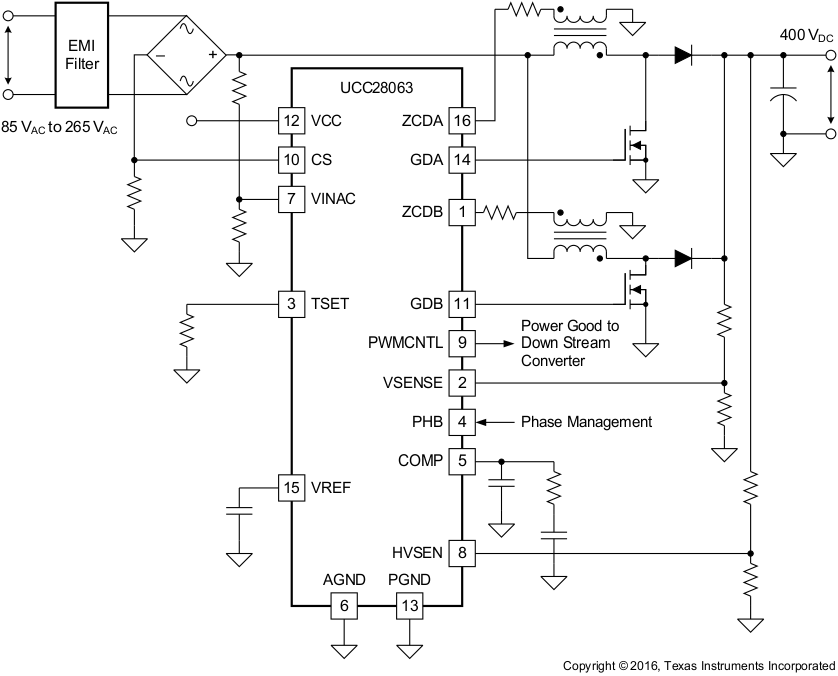
Typical Application Diagram

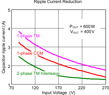
Input Ripple Current Reduction with Interleaving
