JAJSF22D July 2013 – March 2018 UCC28740
PRODUCTION DATA.
- 1 特長
- 2 アプリケーション
- 3 概要
- 4 改訂履歴
- 5 Pin Configuration and Functions
- 6 Specifications
- 7 Detailed Description
-
8 Application and Implementation
- 8.1 Application Information
- 8.2
Typical Application
- 8.2.1 Design Requirements
- 8.2.2
Detailed Design Procedure
- 8.2.2.1 Custom Design With WEBENCH® Tools
- 8.2.2.2 Standby Power Estimate and No-Load Switching Frequency
- 8.2.2.3 Input Bulk Capacitance and Minimum Bulk Voltage
- 8.2.2.4 Transformer Turns-Ratio, Inductance, Primary Peak Current
- 8.2.2.5 Transformer Parameter Verification
- 8.2.2.6 VS Resistor Divider, Line Compensation
- 8.2.2.7 Output Capacitance
- 8.2.2.8 VDD Capacitance, CVDD
- 8.2.2.9 Feedback Network Biasing
- 8.2.3 Application Curves
- 9 Power Supply Recommendations
- 10Layout
- 11デバイスおよびドキュメントのサポート
- 12メカニカル、パッケージ、および注文情報
7.3.2 Valley-Switching and Valley-Skipping
The UCC28740 uses valley-switching to reduce switching losses in the MOSFET, to reduce induced-EMI, and to minimize the turnon current spike at the current-sense resistor. The controller operates in valley-switching in all load conditions unless the VDS ringing diminishes to the point where valleys are no longer detectable.
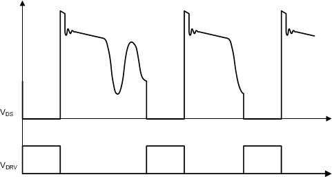
As shown in Figure 11, the UCC28740 operates in a valley-skipping mode (also known as valley-hopping) in most load conditions to maintain an accurate voltage or current regulation point and still switch on the lowest available VDS voltage.
 Figure 11. Valley-Skipping Mode
 Valley-skipping modulates each switching cycle into discrete period durations. During FM operation, the switching cycles are periods when energy is delivered to the output in fixed packets, where the power-per-cycle varies discretely with the switching period. During operating conditions when the switching period is relatively short, such as at high-load and low-line, the average power delivered per cycle varies significantly based on the number of valleys skipped between cycles. As a consequence, valley-skipping adds additional ripple voltage to the output with a frequency and amplitude dependent upon the loop-response of the shunt-regulator. For a load with an average power level between that of cycles with fewer valleys skipped and cycles with more valleys skipped, the voltage-control loop modulates the FB current according to the loop-bandwidth and toggles between longer and shorter switching periods to match the required average output power.