JAJSE40A October 2017 – February 2018 UCC28780
PRODUCTION DATA.
- 1 特長
- 2 アプリケーション
- 3 概要
- 4 改訂履歴
- 5 Pin Configuration and Functions
- 6 Specifications
-
7 Detailed Description
- 7.1 Overview
- 7.2 Functional Block Diagram
- 7.3
Detailed Pin Description
- 7.3.1 BUR Pin (Programmable Burst Mode)
- 7.3.2 FB Pin (Feedback Pin)
- 7.3.3 VDD Pin (Device Bias Supply)
- 7.3.4 REF Pin (Internal 5-V Bias)
- 7.3.5 HVG and SWS Pins
- 7.3.6 RTZ Pin (Sets Delay for Transition Time to Zero)
- 7.3.7 RDM Pin (Sets Synthesized Demagnetization Time for ZVS Tuning)
- 7.3.8 RUN Pin (Driver Enable Pin)
- 7.3.9 SET Pin
- 7.4
Device Functional Modes
- 7.4.1 Adaptive ZVS Control with Auto-Tuning
- 7.4.2 Dead-Time Optimization
- 7.4.3 Control Law across Entire Load Range
- 7.4.4 Adaptive Amplitude Modulation (AAM)
- 7.4.5 Adaptive Burst Mode (ABM)
- 7.4.6 Low Power Mode (LPM)
- 7.4.7 Standby Power Mode (SBP)
- 7.4.8 Startup Sequence
- 7.4.9 Survival Mode of VDD
- 7.4.10 System Fault Protections
- 7.4.11 Pin Open/Short Protections
-
8 Application and Implementation
- 8.1 Application Information
- 8.2
Typical Application Circuit
- 8.2.1 Design Requirements
- 8.2.2 Detailed Design Procedure
- 8.2.3 Application Curves
- 9 Power Supply Recommendations
- 10Layout
- 11デバイスおよびドキュメントのサポート
- 12メカニカル、パッケージ、および注文情報
パッケージ・オプション
デバイスごとのパッケージ図は、PDF版データシートをご参照ください。
メカニカル・データ(パッケージ|ピン)
- D|16
- RTE|16
サーマルパッド・メカニカル・データ
- RTE|16
発注情報
7.3.2 FB Pin (Feedback Pin)
The FB pin connects to the collector of an optocoupler output transistor through an external current-limiting resistor (RFB). Depending on the operating mode, the controller uses different content of the collector current flowing out of the FB pin (IFB) to regulate the output voltage. For the operating modes based on peak current control, IFB is converted into an internal peak current threshold (VCST) to modulate the amplitude of the current sense signal on the CS pin. For example, when the output voltage (VO) is lower than the regulation level set by the shunt regulator, the “current level” of IFB moves to lower value, so VCST goes up to deliver more power to the output load.
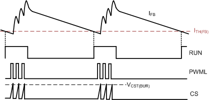
As the burst control takes over the VO regulation, where VCST is clamped to VCST(BUR), the “current ripple” of IFB is used to modulate burst off time, as shown in Figure 13. Specifically, after a group of pulses stop bursting, the output load current starts to discharge the output capacitor, which makes VO start to decay. A proper type-III compensation on the secondary side of VO feedback loop minimizes the phase-delay between IFB current ripple and output voltage ripple. For a detailed design guide on each passive component of the type-III compensator, please refer to Application and Implementation. When the decaying IFB intersects with an internal reference current (ITH(FB)), the ripple regulator generates a new set of grouped burst pulses to deliver more power, which makes VO and IFB ripples move upward.
 Figure 13. Concept of Burst Control
 The nature of ripple-based control in burst mode requires additional care on the noise level of IFB to improve the consistency of burst off-time between burst cycles. Firstly, a high-quality ceramic-bypass capacitor between FB pin and REF pin (CFB) is required for decoupling IFB noise. A minimum of 100 pF is recommended. There is an internal 8-kΩ resistor (RFBI) connected to the FB pin that in conjunction with an external CFB forms an effective low-pass filter. On the other hand, too strong low-pass filtering with too large CFB can attenuate the IFB ripple creating slope distortion of the intersection point between IFB and ITH(FB), which can cause inconsistent burst off-times, even though VO stays in regulation and the IFB noise is low. Secondly, since ABM utilizes the falling-edge burst-ripple content of IFB to determine the beginning of every burst packet, the operation is affected if the burst-ripple content of the output voltage is too small due to using a low-ESR output capacitor, or if there is an additional low-frequency ringing on the output ripple due to using a second-order output filter.
Compared with an electrolytic-type of output capacitor, the advantage of ACF using a low-ESR output capacitor such as a polymer capacitor is to minimize the switching-ripple content of the output voltage to meet the ripple specification, but the burst-ripple content is also reduced. Therefore, the switching ripple and noise on IFB may be very close to ITH(FB), which triggers the next burst event prematurely. For a converter using a second-order output filter, a π filter design as example, even though both switching-ripple and burst-ripple contents are further attenuated, additional low-frequency ringing caused by the resonance between the output filter inductor and one of the output filter capacitors is generated, which may trigger the next burst event too early as well. Therefore, applying an active ripple compensation (ARC) technique is recommended to generate a noise-free burst ripple artificially to stabilize the ABM operation of ACF using either a low-ESR output capacitor or a second-order output filter.
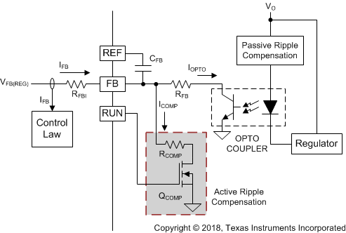
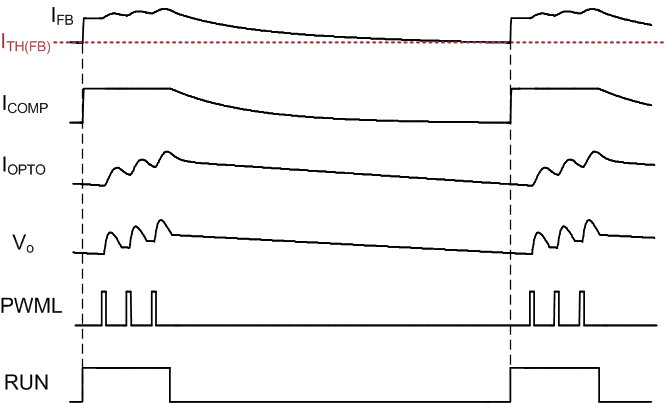
Figure 14 illustrates the implementation of ARC formed by a high-impedance resistor (RCOMP) in series with a small-signal enhancement MOSFET (QCOMP) where its gate is controlled by the RUN pin of UCC28780. When RUN pin is in a high state which turns on QCOMP, RCOMP connected to FB pin creates a compensation current (ICOMP), with a magnitude around VFB / RCOMP. When RUN pin changes to a low state which turns off QCOMP, RCOMP and the drain-source junction capacitor of QCOMP creates a slow falling edge of ICOMP, with a ramp slope dependent on the RC time constant. Then, the summation of the current from the optocoupler (IOPTO) and ICOMP becomes the total feedback current out of FB pin (IFB) to compare with ITH(FB). As the ARC operation in Figure 15 explains, the magnitude of ICOMP helps to push any switching and noise content of IFB away from ITH(FB), and the slow falling edge of ICOMP further pushes the undesirable ripple content away from ITH(FB), especially the low-frequency ringing of the π output filter. The magnitude of ICOMP can be adjusted by RCOMP, and 1 MΩ to 2 MΩ is the recommended value which injects around 2 μA to 4 μA of compensation ripple current into the loop.
 Figure 14. Implementation of Active Ripple Compensation (ARC)
  Figure 15. Concept of Burst Control with ARC