SLUSC05D July   2014  – May 2016 UCC28880

PRODUCTION DATA.  

  1. Features
  2. Applications
  3. Description
  4. Revision History
  5. Pin Configuration and Functions
  6. Specifications
    1. 6.1 Absolute Maximum Ratings
    2. 6.2 ESD Ratings
    3. 6.3 Recommended Operating Conditions
    4. 6.4 Thermal Information
    5. 6.5 Electrical Characteristics
    6. 6.6 Switching Characteristics
    7. 6.7 Typical CharacteristicsTypical Characteristics graphs 1 through 7.
  7. Detailed Description
    1. 7.1 Overview
    2. 7.2 Functional Block Diagram
    3. 7.3 Feature Description
    4. 7.4 Device Functional Modes
      1. 7.4.1 Startup Operation
      2. 7.4.2 Feedback and Voltage Control Loop
      3. 7.4.3 PWM Controller
      4. 7.4.4 Current Limit
      5. 7.4.5 Inductor Current Runaway Protection
      6. 7.4.6 Thermal Shutdown Over-Temperature Protection section to Thermal Shutdown section.
  8. Application and Implementation
    1. 8.1 Application Information
    2. 8.2 Typical Application
      1. 8.2.1 12-V, 100-mA Low-Side Buck Converter
        1. 8.2.1.1 Design Requirements
        2. 8.2.1.2 Detailed Design Procedure
          1. 8.2.1.2.1 Custom Design with WEBENCH Tools
          2. 8.2.1.2.2 Input Stage (RF, D2, D3, C1, C2, L2)
          3. 8.2.1.2.3 Regulator Capacitor (CVDD)
          4. 8.2.1.2.4 Freewheeling Diode (D1)Freewheeling Diode (D1) section.
          5. 8.2.1.2.5 Output Capacitor (CL)
          6. 8.2.1.2.6 Load Resistor (RL)
          7. 8.2.1.2.7 Inductor (L1)
          8. 8.2.1.2.8 Feedback Path (Q1, RFB1, RFB2)
        3. 8.2.1.3 Application Curves
      2. 8.2.2 12-V, 100-mA, High-Side Buck Converter
        1. 8.2.2.1 Design Requirements
        2. 8.2.2.2 Detailed Design Procedure
          1. 8.2.2.2.1 Introduction
          2. 8.2.2.2.2 Feedback Path (CFB, RFB1 and RFB2) and Load Resistor (RL)
        3. 8.2.2.3 Application Curves
      3. 8.2.3 Additional UCC28880 Application Topologies
        1. 8.2.3.1 Low-Side Buck and LED Driver - Direct Feedback (Level Shifted)
        2. 8.2.3.2 12-V, 100-mA High-Side Buck Converter
        3. 8.2.3.3 Non-Isolated, Low-Side Buck-Boost Converter
        4. 8.2.3.4 Non-Isolated, High-Side Buck-Boost Converter
        5. 8.2.3.5 Non-Isolated Flyback Converter
        6. 8.2.3.6 Isolated Flyback Converter
  9. Power Supply Recommendations
  10. 10Layout
    1. 10.1 Layout Guidelines Layout Guidelines section.
    2. 10.2 Layout Example
  11. 11Device and Documentation Support
    1. 11.1 Custom Design with WEBENCH Tools
    2. 11.2 Receiving Notification of Documentation Updates
    3. 11.3 Trademarks
    4. 11.4 Electrostatic Discharge Caution
    5. 11.5 Glossary
  12. 12Mechanical, Packaging, and Orderable Information

パッケージ・オプション

メカニカル・データ(パッケージ|ピン)
サーマルパッド・メカニカル・データ
発注情報

5 Pin Configuration and Functions

D package
8-Pin SOIC
Top View
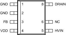
UCC28880 pin_lusc05.gif

Pin Functions

PIN I/O DESCRIPTION
NAME NO.
DRAIN 8 P Drain pin
FB 3 I Feedback terminal
GND 1 G Ground
GND 2 G Ground
HVIN 5 P Supply pin
NC 6 N/C Not internally connected
VDD 4 O Supply pin, supply is provided by internal LDO