SLVSCS1B March 2015 – May 2015 UCD7138
PRODUCTION DATA.
- 1 Features
- 2 Applications
- 3 Description
- 4 Simplified Schematic
- 5 Revision History
- 6 Pin Configuration and Functions
- 7 Specifications
- 8 Detailed Description
- 9 Application and Implementation
- 10Power Supply Recommendations
- 11Layout
- 12Device and Documentation Support
- 13Mechanical, Packaging, and Orderable Information
9 Application and Implementation
NOTE
Information in the following applications sections is not part of the TI component specification, and TI does not warrant its accuracy or completeness. TI’s customers are responsible for determining suitability of components for their purposes. Customers should validate and test their design implementation to confirm system functionality.
9.1 Application Information
The UCD7138 device can be used in a wide range of applications. The device can be used on many center-tapped secondary-side rectification topologies. Specifically, the device can be used in half-bridge LLC converters. In these applications, the UCD3138A and UCD7138 chipset enables the synchronous rectifiers to closely approximate the behavior of an ideal diode which is difficult to do in an LLC converter because of the variations in the SR current-conduction time.
The UCD7138 and UCD3138A chipset together can provide an easy-to-use, high-performance and advanced SR-control solution. Without this solution, fine tuning is required for each operation region (including below resonant frequency, at resonant frequency, and above resonant frequency). For LLC converters in production, each power stage may have a different resonant frequency because of tolerances of circuit capacitors and inductors. Calibration is required for each converter to achieve high efficiency. With UCD7138 and UCD3138A advanced SR control, optimal SR operation is easily achieved for every converter without fine tuning and calibration of the resonant tank can be eliminated in production. For more information see Using UCD7138 and UCD3138A for Advanced Synchronous Rectification Control, SLUA737.
9.2 Typical Application
9.2.1 Half-Bridge LLC
Figure 27 shows a typical half-bridge LLC application using the UCD7138 device as a secondary-side SR driver and the UCD3138A device as a controller.
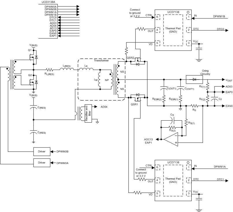 Figure 27. Half-Bridge LLC Typical Application Diagram
In LLC converters, if the SRs are not well optimized, the SR conduction time can either be too long or too short. The duration of the body diode conduction time can be determined by examining the drain-to-source voltage of the MOSFET when it is off. The SR turnon edge is optimized by the UCD7138 device by turning the gate on as soon as body-diode conduction is sensed. The SR turnoff edge is determined when the UCD3138A digital controller analyzes the sensed body-diode conduction time. Figure 28 shows the typical drain-to-source waveforms on a half-bridge LLC converter and the desired waveforms.
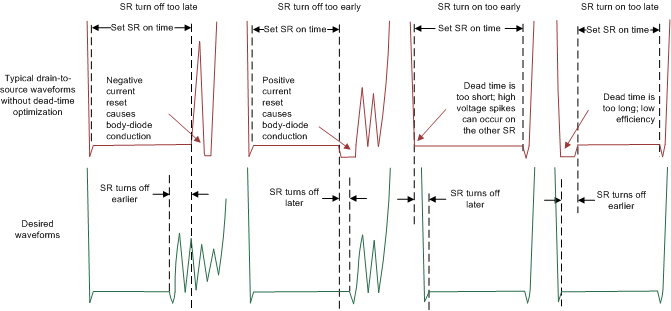 Figure 28. Drain to Source Voltage Waveforms in a Typical Half Bridge LLC Application and Desired Waveforms
As shown in Figure 29, when the SR pulse is on for too long, the drain-to-source voltage shoots up. The upper waveform in Figure 29 shows the SR current. The lower waveform shows the SR drain-to-source voltage. The black segment of the curves show when the SR MOSFET is on. The red and green segments of the curves show when the SR MOSFET is off. The SR current is positive at first, but continues to drop until it is negative. The drain-to-source voltage is close to 0 V when the SR MOSFET is on. As soon as the SR MOSFET is turned off, the negative current must reset. The capacitance across the drain and source terminal is charged, and the drain-to-source voltage increases. The green segments of the curves show when the negative current reset process is complete at which point the body diode of the MOSFET conducts briefly again.
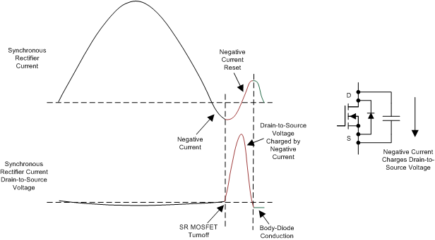 Figure 29. SR Drain-to-Source Voltage Shoot Up When No Negative Current Flow Occurs
For the UCD3138A device, a DTC detection window is generated at the falling edge of the gate drive command IN signal. Only during this detection window is the DTC low time counted by a 4-ns resolution timer capture inside the UCD3138A device. Figure 30 shows the simplified system block diagram. In the two body-diode conduction cases shown in Figure 31, the SR on time should be adjusted in different directions. The detection window identify that these two cases are different. If, during the detection window, a large amount of DTC low time is detected, and the SR turns off too early. If, during the detection window, no or very-short DTC low time is detected and the SR turns off too late.
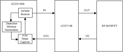 Figure 30. Simplified System Block Diagram
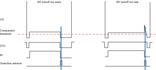 Figure 31. Body-Diode Connection Detection
The UCD3138A digital controller counts the body-diode conduction time of the current cycle and adjusts the SR on time of the next cycle. In Figure 32, the DTC0 and DTC1 signals are the body-diode conduction inputs received from the UCD7138 device. SR0_DPWM and SR1_DPWM are the DPWM waveforms for the SRs. The red and green dashed lines are moving edges controlled by both the UCD3138A digital-compensator output and the DTC interface. In each cycle, directly after the falling edge of the SR DPWM waveform, a detection window is generated for the body-diode conduction time. The detection window is defined by both DETECT_BLANK and DETECT_LEN registers. During this detection window, a 4-ns timer capture counts the conduction time of the body diode. The SR DPWM turnoff edge of the next cycle is then adjusted accordingly.
 Figure 32. Timing Diagram of the DTC Interface in UCD3138A
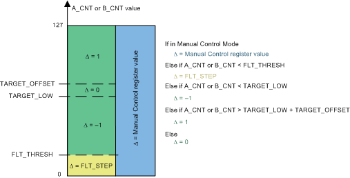 Figure 33. DTC Interface Principle
Figure 33 shows how the SR turnoff edge is adjusted based on the DTC measurement of the previous cycle. The A_CNT or B_CNT is the counted values of diode conduction time of two SRs which ranges from 0 to 127. The two types of SR control modes are automatic-control mode and manual-control mode. If manual-control mode is used, the SR on-time adjustment value is determined by the manual write register. If automatic-control mode is used, the UCD3138A digital controller automatically calculates the SR on-time adjustment amount for the next cycle. The body-diode conduction time at the falling edge of the SR gate is regulated to a target value by step-by-step edge adjustment in the UCD3138A device. The SR on time is reduced by a preprogrammed large amount, when the sensed body-diode conduction time is less than a programmable threshold. This reduction prevents the power supply from damaged caused by negative current in the SRs.
For more information on the DTC interface on UCD3138A see UCD7138 and UCD3138A for Advanced Synchronous Rectification Control, SLAU737 and UCD3138A Highly Integrated Digital Controller for Isolated Power, SLUSC66.
9.2.1.1 Design Requirements
9.2.1.1.1 Gate Input
The input stage of the driver should be driven by a signal with fast rise and fall times. Caution must be exercised whenever the driver is used with slowly varying input signals, in situations where the device is located in a mechanical socket or PCB layout is not optimal (bad grounding, for example). Ground bounce is often caused by high di/dt current from the driver output, coupled with board-layout parasitic. The differential voltage between the input pin IN and ground pad GND may be modified by ground bounce and trigger an unintended change of output state. Because of short propagation delay, the unintended change of state can ultimately result in high-frequency oscillations, which increases power dissipation and can potentially damage the device. In the worst case, when a slow input signal is used and PCB layout is not optimal, adding a small capacitor (1 nF) between the input pin and ground very close to the driver device may be necessary.
9.2.1.1.2 Gate Output
The output of the gate driver (OUT) must be connected as close to the MOSFET gate as possible. A small resistor may be connected in between to reduce the high-frequency oscillations on the gate. Doing so can also slow down the gate transitions. The DTC detection windows inside UCD3138A may need some adjustment to compensate for the delay caused by the added resistor.
9.2.1.1.3 Drain-to-Source Voltage Sensing
When the drain-to-source voltage is below 0 V, current flows out of the VD pin to the drain terminal of the MOSFET. This current flow must be limited to ensure proper operation of the device. The recommended current-limiting resistance value is 20Ω.
The highest voltage that can be applied to VD pin is 45 V which is good for applications where 40-V MOSFETs are used for the secondary-side SRs. If a higher voltage is required for VD pin, an external high-voltage blocking circuit can be used together with the UCD7138 device as shown in Figure 34. Depending on the required voltage rating, a different external high-voltage blocking MOSFET can be selected. Usually a small SOT-23 MOSFET can be used. In this circuit, the gate terminal of the external high-voltage blocking MOSFET is connected to VCC of the UCD7138 gate driver. The source terminal is connected with a current-limiting resistor to the VD pin of the UCD7138 device. The drain terminal is connected to the SR MOSFET drain terminal. When a low voltage is presented at the drain terminal, the blocking MOSFET is turned on because of the positive gate-to-source voltage. When the drain voltage becomes higher and higher, the source terminal voltage rises along with the drain terminal until the gate-to-source voltage falls below the threshold. When the source voltage is high enough so that the blocking MOSFET is turned off, the high voltage on the SR drain is blocked.
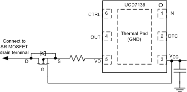 Figure 34. External High-Voltage Blocking Circuit
9.2.1.1.4 DTC Output
The DTC pin is the internal comparator output. This pin should be connected to the DTC0 or DTC1 pin on the UCD3138A device. To keep edges sharp, no filtering is recommended. If noise spikes are observed on the DTC signal, the blanking times in the UCD3138A device can be used to prevent the digital controller from sensing noise. This pin is not designed to drive large current. If filtering must be used, ensure that the sink and source current on this pin is within ±4 mA as specified in the
Electrical Characteristics table.
9.2.1.1.5 Turn-on Edge Optimization
The turnon edge optimization is useful when a positive current flow is at the rising edge of SRs. To maximize the efficiency gain, the dead time between the falling edge of the primary and the rising edge of the secondary should be programmed to a smaller value than expected, so that the rising edge of the SRs can move freely by UCD7138.
9.2.1.2 Detailed Design Procedure
9.2.1.2.1 Design Without SR-Control Optimization
The design procedure of an LLC converter with synchronous rectification can be greatly simplified by using the UCD7138 and UCD3138A chipset. The converter hardware and firmware can initially be designed without advanced SR optimization and then add SR optimization function in.
For more information on the UCD3138A-based digital LLC converter, UCD3138A Highly Integrated Digital Controller for Isolated Power, SLUSC66.
9.2.1.2.2 Setting the DTC Detection Window
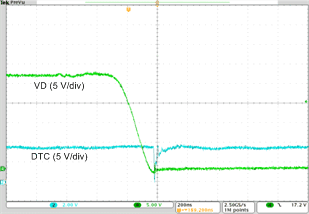
The body-diode conduction should be detected in a specific region for the system to operate correctly. The detection window is defined by a blanking time register DETECT_BLANK and a detection length register DETECT_LEN in the UCD3138A device. To set the detection window, let the LLC converter operate below resonant frequency. measure the VD, IN, and DTC waveforms on an oscilloscope. Use cursors to measure the time, t, difference between the IN falling edge and the starting point of body-diode conduction (first falling edge of DTC excluding noise spike). The blanking time should be set to be less than t. Usually the required blanking time is very short or non existent, so the blanking time can be set to around 10% of t. The detection window length can be set to a few times of the desired body-diode conduction time. For example, if the desired body-diode conduction time is 40 ns, the detection window length can be set to 120 ns. Make sure that the body-diode conduction is well covered inside the detection window when it is at an optimal value. The end point of the detection window should never exceed the first valley on the VD waveform to avoid errors in measurement (see Figure 35).
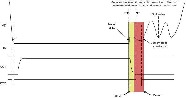 Figure 35. Setting the DTC Detection Window in UCD3138A
After the detection window is set, enable the DTC module in manual control mode. Set the offset in the manual control registers to 0. Change the input voltage and load current to different operation points to verify that the UCD3138A DTC module measures the correct values in the A_CNT and B_CNT registers. See the UCD3138A64 Programmer’s Manual, SLUUB54 for detailed register information.
9.2.1.2.3 Setting the Clamps
The SR adjustment accumulator clamps defines the maximum SR turnoff edge offset from the calculated value from the UCD3138A compensator. The maximum clamp can be set to prevent the SR on time from going too long and causing shoot through. The minimum clamp can be set based on the light load condition where the desired SR turnoff edge offset is the maximum.
In addition to the SR adjustment accumulator clamps, the SR pulse falling edge is naturally clamped at 50% or 100% or the switching period in UCD3138A. This natural clamp is a default feature of UCD3138A and does not require any special setting.
9.2.1.2.4 Setting the DTC Optimization Target and Hysteresis
The body diode must maintain a minimum conduction time for the UCD3138A DTC interface to function properly. The minimum body-diode conduction time is set by the DTC target and target register. A target hysteresis register can also be set to reduce the steady-state output-voltage ripple.
9.2.1.2.5 Setting the DTC Negative Current Fault Protection
If the detected body-diode conduction time is less than the programmed threshold, negative current can occur. This threshold can be set by the fault threshold register in the UCD3138A DTC module. If a DTC fault is detected, the SR on time is reduced by a programed step size in the next switching cycle. This step size is defined by FLT_STEP register in the DTC module. To avoid noise and jitter in the negative current fault detection, a consecutive DTC fault counter can be used. A fault step is executed only after a consecutive number of faults are detected.
After all these registers are set, enable the UCD3138A DTC module in automatic control mode, enable the turnon-edge optimization on the UCD7138 device, and review the different operation conditions to see the overall system performance. The DTC module can be turned on or off by toggling DTC_EN bit in Loop Mux register in UCD3138A. The performance before and after SR optimization control can be compared very easily as shown in the Application Curves section.
9.2.1.3 Application Curves
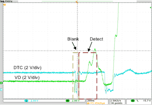
| No optimization, SR on time too long. | ||
| High VDS stress on the other SR. | ||
| Horizontal: 200 ns/div |
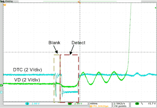
| No optimization, SR on time too short. Low efficiency. | ||
| Horizontal: 200 ns/div |
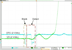
| With optimization | ||
| Horizontal: 200 ns/div | ||
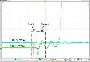
| With optimization | ||
| Horizontal: 200 ns/div |
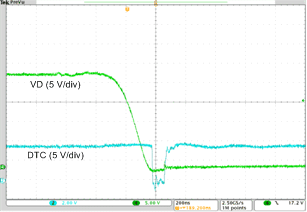
| No optimization, SR on turnon too late. Low efficiency. | ||
| Horizontal: 200 ns/div |
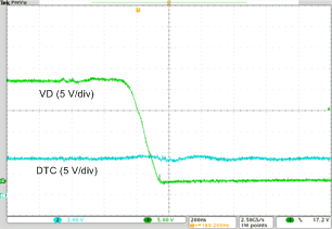
| No optimization, SR turnon too early. | ||
| Horizontal: 200 ns/div |
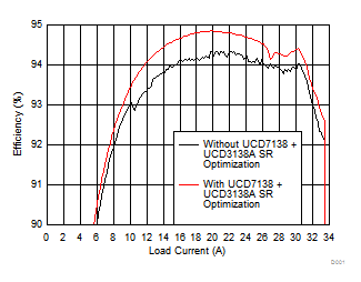
| Efficiency increase at peak efficiency: 0.54% | Peak efficiency increase (occurs at no-load): 2.62% | ||
| Average efficiency increase over constant voltage load range: 0.63% | |||
| Peak efficiency with and without SR optimization: 94.85% at 19.92 A | |||
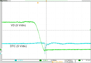
| With optimization | ||
| Horizontal: 200 ns/div |
| With optimization | ||
| Horizontal: 200 ns/div |