SLVSCS1B March 2015 – May 2015 UCD7138
PRODUCTION DATA.
- 1 Features
- 2 Applications
- 3 Description
- 4 Simplified Schematic
- 5 Revision History
- 6 Pin Configuration and Functions
- 7 Specifications
- 8 Detailed Description
- 9 Application and Implementation
- 10Power Supply Recommendations
- 11Layout
- 12Device and Documentation Support
- 13Mechanical, Packaging, and Orderable Information
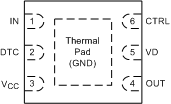
6 Pin Configuration and Functions
DRS Package
6-Pin WSON With Exposed Thermal Pad
Top View

Pin Functions
| PIN | TYPE | DESCRIPTION | |
|---|---|---|---|
| NO. | NAME | ||
| 1 | IN | I | Input: Gate driver input. This pin should be connected directly to the DPWM output of the digital controller. |
| 2 | DTC | O | Body-diode conduction-time report: Standard digital IO. Pulled high internally. Output low when the body diode is conducting. This pin should be connected to the DTC0 or DTC1 pin on UCD3138A. |
| 3 | VCC | P | IC supply: External bias supply input. The supply range is 4.5-V to 18-V. A ceramic bypass capacitor of at least 1 µF should be placed as close as possible to the VCC pin and the thermal pad. Where possible, use thick & wide Cu connections. |
| 4 | OUT | O | Gate driver output: Integrated push-pull gate driver for one or more external power MOSFETs. Typical 4-A source and 6-A sink capability. This is a rail-to-rail output, with the rails defined by the voltages on VCC and GND. This pin should be connected to the gate terminal of the synchronous rectification MOSFET. |
| 5 | VD | I | Drain voltage: Connect this pin as close as possible to the controlled-MOSFET drain pad. This pin is internally connected to the diode conduction detection comparator. The comparator has a –0.15-V threshold to detect body-diode conduction. A 20-Ω resistor should be connected between the VD pin and MOSFET drain terminal to limit the current. The maximum voltage of the VD pin should not exceed 45 V. A simple external circuit can enable the usage of much higher voltages, see Figure 34. |
| 6 | CTRL | I | Rising edge optimization control: Connect this pin to ground to disable rising edge optimization. Leave this pin floating or connect it to logic high to enable rising edge optimization. |
| — | Thermal Pad (GND) | — | Exposed thermal pad: The exposed pad on the bottom of the package enhances the thermal performance of the device. This pad is the device ground reference. |