JAJSDE5 June 2017
PRODUCTION DATA.
- 1 特長
- 2 アプリケーション
- 3 概要
- 4 改訂履歴
- 5 Pin Configuration and Functions
- 6 Specifications
- 7 Detailed Description
- 8 Application and Implementation
- 9 Power Supply Recommendations
- 10Layout
- 11デバイスおよびドキュメントのサポート
- 12メカニカル、パッケージ、および注文情報
8 Application and Implementation
NOTE
Information in the following applications sections is not part of the TI component specification, and TI does not warrant its accuracy or completeness. TI’s customers are responsible for determining suitability of components for their purposes. Customers should validate and test their design implementation to confirm system functionality.
8.1 Application Information
The LF442-MIL uses a combination of careful layout design and internal trimming to ensure very low input offset voltage and voltage drift. The LF442-MIL also has a very low equivalent input noise voltage for a low power amplifier. The LF442-MIL should be used where low power dissipation and good electrical characteristics are the major considerations.
8.2 Typical Applications
- Battery Powered Strip Chart Preamplifier
- "No FET" Low Power V to F Converter
- High Efficiency Crystal Oven Controller
- Conventional Log Amplifier
- Unconvential Log Amplifier
8.2.1 Battery Powered Strip Chart Preamplifier
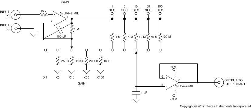 Figure 28. Battery Powered Strip Chart Preamplifier
8.2.1.1 Design Requirements
Runs from 9V batteries (±9V supplies).
Fully set gain and time constant.
Battery powered supply allows direct plug-in interface to strip chart recorder without common-mode problems.
8.2.1.2 Detailed Design Procedure
This device is a dual low power op amp with internally trimmed input offset voltages and JFET input devices (BI-FET II). These JFETs have large reverse breakdown voltages from gate to source and drain eliminating the need for clamps across the inputs. Therefore, large differential input voltages can easily be accommodated without a large increase in input current. The maximum differential input voltage is independent of the supply voltages. However, neither of the input voltages should be allowed to exceed the negative supply as this will cause large currents to flow which can result in a destroyed unit.
Exceeding the negative common-mode limit on either input will force the output to a high state, potentially causing a reversal of phase to the output. Exceeding the negative common-mode limit on both inputs will force the amplifier output to a high state. In neither case does a latch occur since raising the input back within the common-mode range again puts the input stage and thus the amplifier in a normal operating mode.
Exceeding the positive common-mode limit on a single input will not change the phase of the output; however, if both inputs exceed the limit, the output of the amplifier will be forced to a high state.
The amplifiers will operate with a common-mode input voltage equal to the positive supply; however, the gain bandwidth and slew rate may be decreased in this condition. When the negative common-mode voltage swings to within 3V of the negative supply, an increase in input offset voltage may occur.
Each amplifier is individually biased to allow normal circuit operation with power supplies of ±3.0V. Supply voltages less than these may degrade the common-mode rejection and restrict the output voltage swing.
The amplifiers will drive a 10 kΩ load resistance to ± 10V over the full temperature range.
Precautions should be taken to ensure that the power supply for the integrated circuit never becomes reversed in polarity or that the unit is not inadvertently installed backwards in a socket as an unlimited current surge through the resulting forward diode within the IC could cause fusing of the internal conductors and result in a destroyed unit.
A feedback pole is created when the feedback around any amplifier is resistive. The parallel resistance and capacitance from the input of the device (usually the inverting input) to AC ground set the frequency of the pole. In many instances the frequency of this pole is much greater than the expected 3 dB frequency of the closed loop gain and consequently there is negligible effect on stability margin. However, if the feedback pole is less than approximately 6 times the expected 3 dB frequency a lead capacitor should be placed from the output to the input of the op amp. The value of the added capacitor should be such that the RC time constant of this capacitor and the resistance it parallels is greater than or equal to the original feedback pole time constant.
8.2.1.3 Application Curves
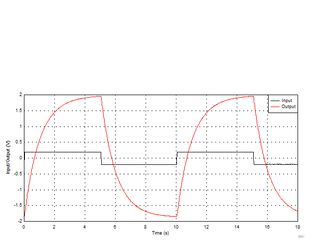 Figure 29. Input and Output Waveforms, Gain = 10, Time Constant = 1 Second
8.2.2 "No FET" Low Power V to F Converter
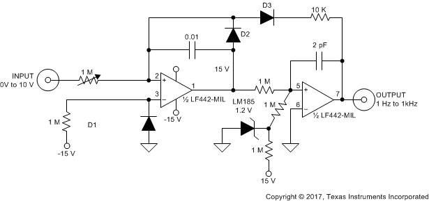 Figure 30. "No FET" Low Power V to F Converter
8.2.2.1 Design Requirements
- Trim 1M pot for 1 kHz full-scale output.
- 15 mW power drain.
- No integrator reset FET required.
- Mount D1 and D2 in close proximity.
- 1% linearity to 1 kHz.
8.2.2.2 Detailed Design Procedure
See Section 8.2.1.2.
8.2.2.3 Application Curves
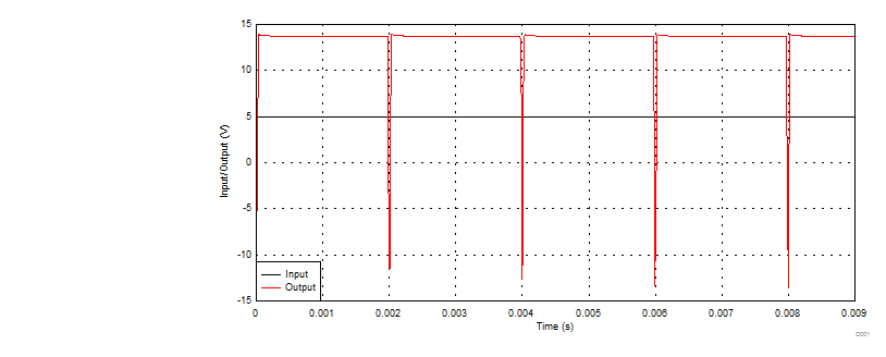 Figure 31. Input and Output Waveforms
8.2.3 High Efficiency Crystal Oven Controller
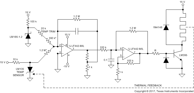 Figure 32. High Efficiency Crystal Oven Controller
8.2.3.1 Design Requirements
- Tcontrol= 75°C
- A1's output represents the amplified difference between the LM335 temperature sensor and the crystal oven's temperature.
- A2, a free running duty cycle modulator, drives the LM395 to complete a servo loop.
- Switched mode operation yields high efficiency.
- 1% metal film resistor.
8.2.3.2 Detailed Design Procedure
See Section 8.2.1.2.
8.2.4 Conventional Log Amplifier
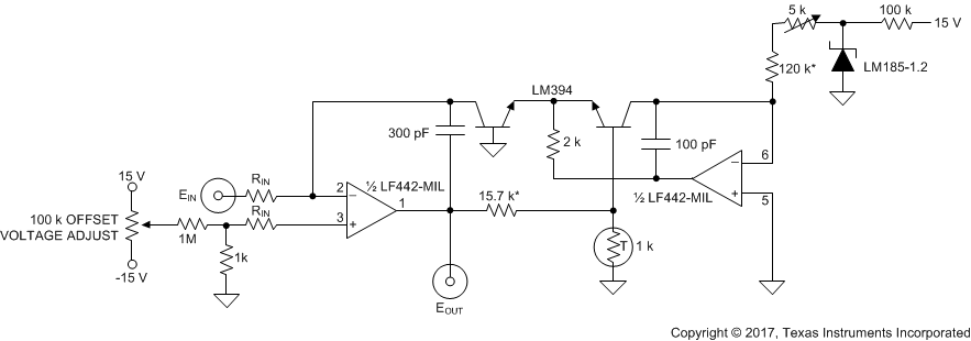 Figure 33. Conventional Log Amplifier
8.2.4.1 Design Requirements
- RT = Tel Labs type Q81.
- Trim 5k for 10 μA through the 5k–120k combination.
- *1% film resistor
8.2.4.2 Detailed Design Procedure
See Section 8.2.1.2.
8.2.5 Unconventional Log Amplifier
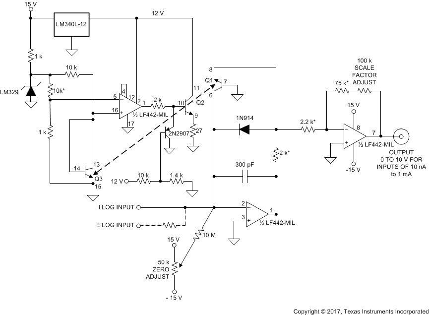 Figure 34. Unconventional Log Amplifier
8.2.5.1 Design Requirements
- Q1, Q2, Q3 are included on LM389 amplifier chip which is temperature-stabilized by the LM389 and Q2-Q3, which act as a heater-sensor pair.
- Q1, the logging transistor, is thus immune to ambient temperature variation and requires no temperature compensation at all.
8.2.5.2 Detailed Design Procedure
See Section 8.2.1.2.