SNOS965J June 2001 – December 2015 LM2611
PRODUCTION DATA.
- 1 Features
- 2 Applications
- 3 Description
- 4 Revision History
- 5 Pin Configuration and Functions
- 6 Specifications
- 7 Detailed Description
-
8 Application and Implementation
- 8.1 Application Information
- 8.2 Typical Application
- 9 Power Supply Recommendations
- 10Layout
- 11Device and Documentation Support
- 12Mechanical, Packaging, and Orderable Information
8 Application and Implementation
NOTE
Information in the following applications sections is not part of the TI component specification, and TI does not warrant its accuracy or completeness. TI’s customers are responsible for determining suitability of components for their purposes. Customers should validate and test their design implementation to confirm system functionality.
8.1 Application Information
The LM2611 is a Cuk controller with an integrated switch. The following section provides an approach to sizing the components for the target application and shows some typical examples of applications to help the designer.
8.2 Typical Application
8.2.1 Cuk Converter With Integrated Switch
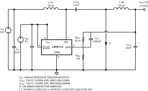 Figure 21. Typical Cuk Converter Implementation Using LM26211
8.2.1.1 Design Requirements
The first variables needed are the output voltage and the input voltage range (min to max). The input voltage range ensures that the IC is suitable for the application and that the absolute maximum voltage are respected. The expected maximum output current is also needed to verify that the IC can deliver the required current.
8.2.1.2 Detailed Design Procedure
The first components to choose are the power inductors. Typically a smaller inductance yields a smaller solution footprint and lower cost but the higher ripple makes a smaller inductance not compatible with every application. Due to the internal compensation, TI recommends a 10-µH to 22-µH inductor. Try to choose the inductors so that the peak-to-peak ripple is lower than 0.3 A of the average current by using Equation 3 and Equation 5.
Using the maximum output current and the input voltage range, calculate the worst case peak current in the switch using Equation 6. If the peak current is above the peak current limit for this part, consider increasing the inductance and re-calculate. If the inductance is above 22 µH for each inductor, the designer will have to pay special attention to stability over the extended range of operation (it's always a good practice to do so even if the inductance is within the recommended range).
Using the desired output voltage, calculate the value of the feedback resistors. The reference voltage is 1.23 V. Resistors of 50 kΩ or less must be used due to the leakage at the NFB pin.
It is a good idea to add a placeholder for a small capacitor across the top feedback resistor to act as a feed-forward component to optimize transient response. Optimization of the feed-forward capacitor depends a lot on the specific parameters including the parasitic components associated with the capacitors. Experimentation is key to ensure ideal sizing of the capacitor (either using load transient response or a loop response analyzer). See Improving Transient Response and Compensation for details regarding the CFF capacitor.
8.2.1.3 Application Curves
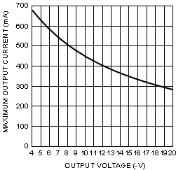 Figure 22. Maximum Output Current vs Output Voltage at VIN = 12 V (L1 = L2 = 22 µH)
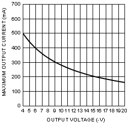 Figure 23. Maximum Output Current vs Output Voltage at VIN = 5 V (L1 = L2 = 22 µH)
8.2.2 5-V to –5-V Inverting Converter
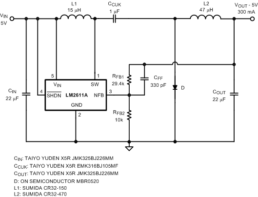 Figure 24. 5-V to –5-V Inverting Converter Schematic
8.2.2.1 Design Requirements
This design converts 5 V (VIN) to –5 V (VOUT). Adjust RFB2 to set a different output voltage.
8.2.2.2 Application Curves
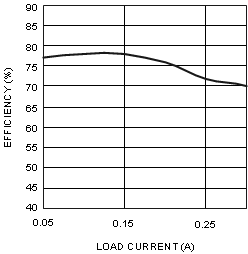 Figure 25. Efficiency vs Load Current
 Figure 26. Maximum Output Current vs Output Voltage, 5 V to –5 V
8.2.3 9-V to –5-V Inverting Converter
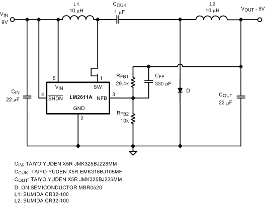 Figure 27. 9-V to –5-V Inverting Converter Schematic
8.2.3.1 Design Requirements
This design converts 9 V (VIN) to –5 V (VOUT). Adjust RFB2 to set a different output voltage.
8.2.3.2 Application Curve
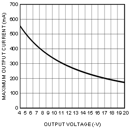 Figure 28. Maximum Output Current vs Output Voltage, 9 V to – 5 V
8.2.4 12-V to –5-V Inverting Converter
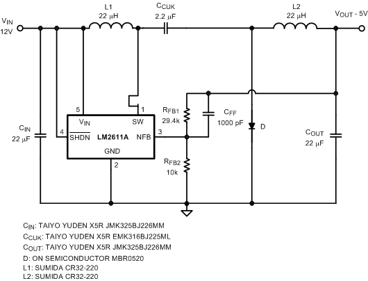
8.2.4.1 Design Requirements
This design converts 12 V (VIN) to –5 V (VOUT). Adjust RFB2 to set a different output voltage.
8.2.4.2 Application Curve
 Figure 30. Maximum Output Current vs Output Voltage, 12 V to –5 V
8.2.5 LM2611 Operating With Separate Power and Biasing Supplies
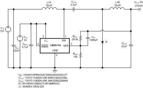 Figure 31. LM2611 Operating With Separate Power and Biasing Supplies Schematic
8.2.5.1 Design Requirements
Follow the design requirements in Cuk Converter With Integrated Switch.
8.2.5.2 Detailed Design Procedure
8.2.5.2.1 Split Supply Operation
The LM2611 may be operated with separate power and bias supplies. In the circuit shown in Figure 31, VIN is the power supply that the regulated voltage is derived from, and VDD is a low current supply used to bias the LM2611. Equation 12 and Equation 13 show the conditions for the supplies are:
As the input voltage increases, the maximum output current capacbility increases. Using a separate, higher voltage supply for power conversion enables the LM2611 to provide higher output currents than it would with a single supply that is limited in voltage by VIN(MAX).
8.2.6 Shutdown and Soft-Start
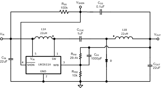 Figure 32. LM2611 Soft-Start Circuit
8.2.6.1 Design Requirements
Follow the design requirements in Cuk Converter With Integrated Switch.
8.2.6.2 Detailed Design Procedure
8.2.6.2.1 Shutdown and Soft-Start
A soft-start circuit is used in switching power supplies to limit the input inrush current upon start-up. Without a soft-start circuit, the inrush current can be several times the steady-state load current, and thus apply unnecessary stress to the input source. The LM2611 does not have soft-start circuitry, but implementing the circuit in Figure 32 lowers the peak inrush current. The SHDN pin is coupled to the output through CSS. The LM2611 is toggled between shutdown and run states while the output slowly decreases to its steady-state value. The energy required to reach steady state is spread over a longer time and the input current spikes decrease (see Figure 33 and Figure 34).
8.2.6.3 Application Curves
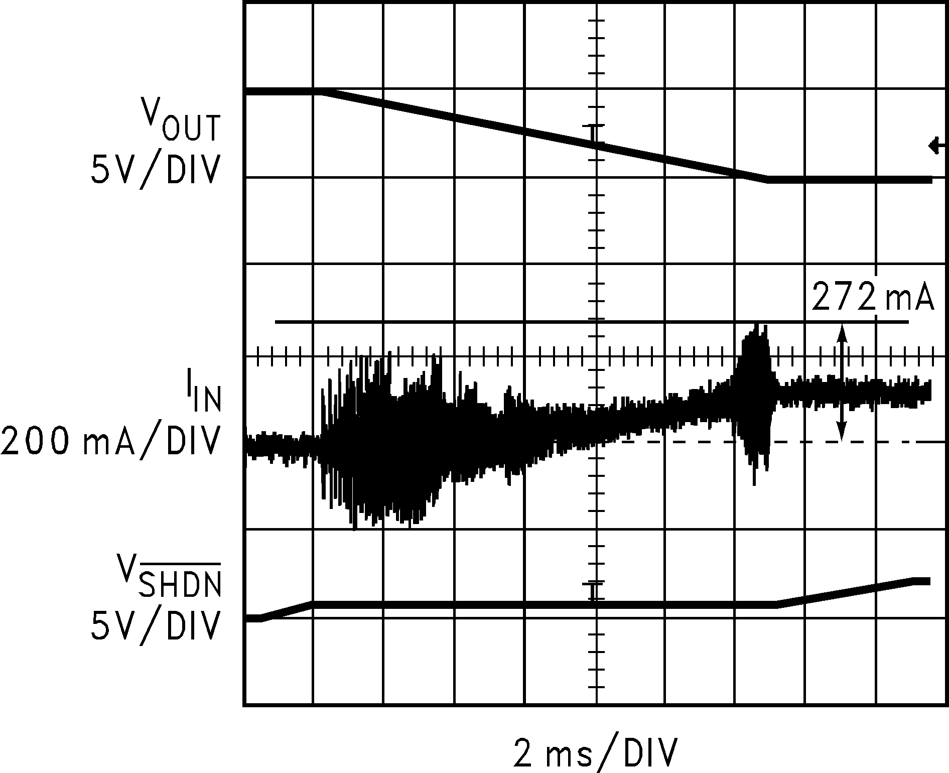 Figure 33. Start-Up Waveforms With a Soft-Start Circuit
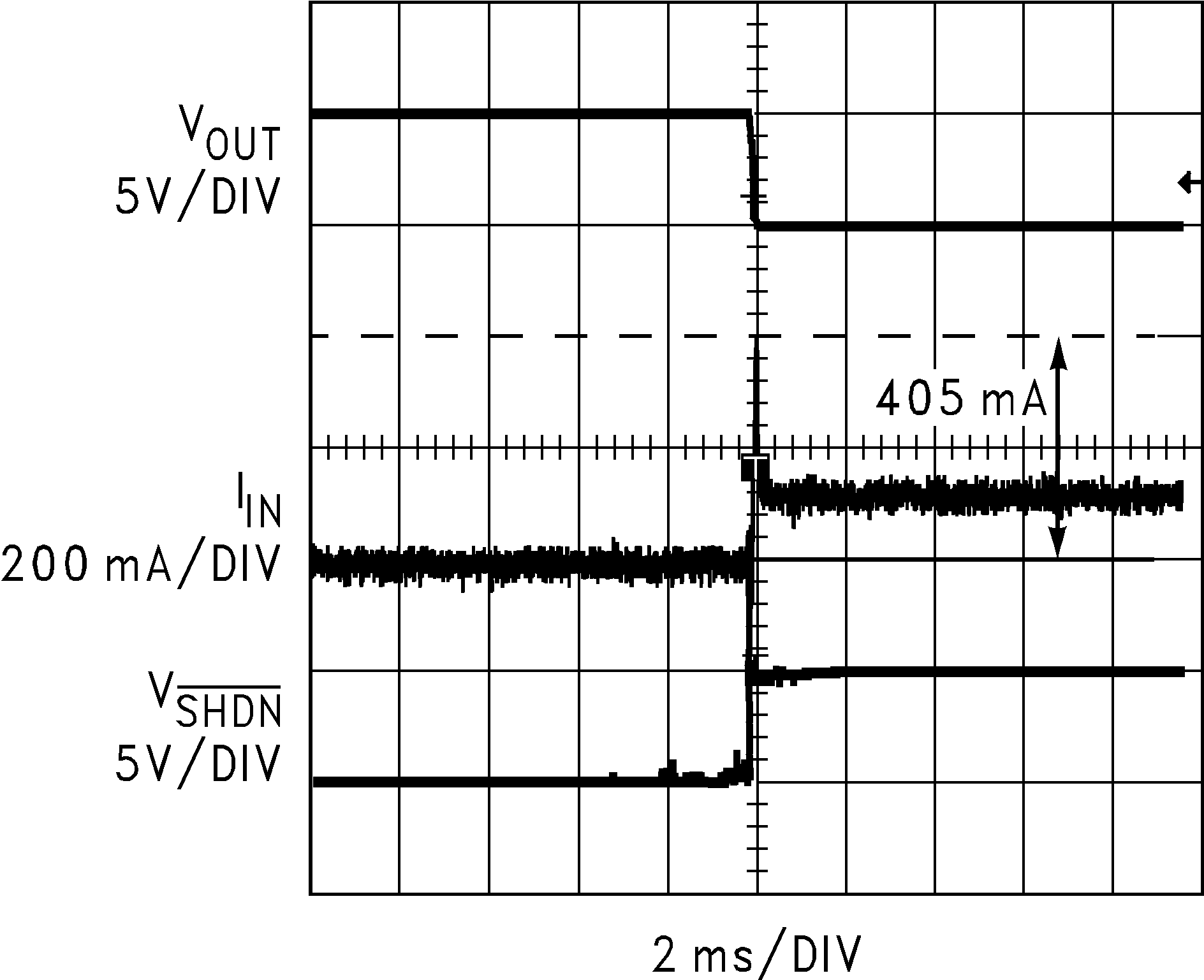 Figure 34. Start-Up Waveforms Without a Soft-Start Circuit
8.2.7 High Duty Cycle and Load Current
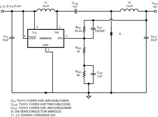 Figure 35. LM2611 High Current Schematic
8.2.7.1 Design Requirements
Follow the design requirements in Cuk Converter With Integrated Switch.
8.2.7.2 Detailed Design Procedure
8.2.7.2.1 High Duty Cycle and Load Current Operation
The circuit in Figure 35 is used for high duty cycles (D > 0.5) and high load currents. The duty cycle begins to increase beyond 50% as the input voltage drops below the absolute magnitude of the output voltage. RFB3 and CFF2 are added to the feedback network to introduce a low frequency lag compensation (pole-zero pair) necessary to stabilize the circuit under the combination of high duty cycle and high load currents.