SNOS965J June 2001 – December 2015 LM2611
PRODUCTION DATA.
- 1 Features
- 2 Applications
- 3 Description
- 4 Revision History
- 5 Pin Configuration and Functions
- 6 Specifications
- 7 Detailed Description
-
8 Application and Implementation
- 8.1 Application Information
- 8.2 Typical Application
- 9 Power Supply Recommendations
- 10Layout
- 11Device and Documentation Support
- 12Mechanical, Packaging, and Orderable Information
7 Detailed Description
7.1 Overview
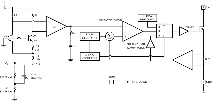
The LM2611 consists of a current mode controller with an integrated primary switch and integrated current sensing circuitry. The feedback is connected to the internal error amplifier and a type II/III internal compensation scheme is used. A ramp generator provides some slope compensation to the system. SHDN pin is a logic input designed to shut down the converter.
7.2 Functional Block Diagram
7.3 Feature Description
7.3.1 Cuk Converter
 Figure 13. Operating Cycles of a Cuk Converter
The LM2611 is a current mode, fixed frequency PWM switching regulator with a −1.23-V reference that makes it ideal for use in a Cuk converter. The Cuk converter inverts the input and can step up or step down the absolute value. Using inductors on both the input and output, the Cuk converter produces very little input and output current ripple. This is a significant advantage over other inverting topologies such as the buck-boost and flyback.
The operating states of the Cuk converter are shown in Figure 13. During the first cycle, the transistor switch is closed and the diode is open. L1 is charged by the source and L2 is charged by CCUK, while the output current is provided by L2. In the second cycle, L1 charges CCUK and L2 discharges through the load. By applying the volt-second balance to either of the inductors, use Equation 1 to determine the relationship of VOUT to the duty cycle (D).

The following sections review the steady-state design of the LM2611 Cuk converter.
7.3.2 Output and Input Inductor
Figure 14 and Figure 15 show the steady-state voltage and current waveforms for L1 and L2, respectively. Referring to Figure 13 (a), when the switch is closed, VIN is applied across L1. In the next cycle, the switch opens and the diode becomes forward biased, and VOUT is applied across L1 (the voltage across CCUK is VIN − VOUT.)
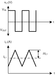 Figure 14. Voltage and Current Waveforms in Inductor L1 of a Cuk Converter
The voltage and current waveforms of inductor L2 are shown in Figure 15. During the first cycle of operation, when the switch is closed, VIN is applied across L2. When the switch opens, VOUT is applied across L2.
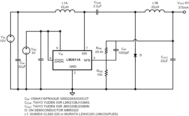 Figure 15. Schematic of the Cuk Converter Using LM2611
Equation 2 to Equation 5 define the values given in Figure 14 and Figure 15:


Use these equations to choose correct core sizes for the inductors. The design of the LM2611's internal compensation assumes L1 and L2 are equal to 10 to 22 µH, thus TI recommends staying within this range.
7.3.3 Switch Current Limit
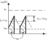
The LM2611 incorporates a separate current limit comparator, making current limit independent of any other variables. The current limit comparator measures the switch current versus a reference that represents current limit. If at any time the switch current surpasses the current limit, the switch opens until the next switching period. To determine the maximum load for a given set of conditions, both the input and output inductor currents must be considered. The switch current is equal to iL1 + iL2, and is drawn in Figure 16. In summary, Equation 6 shows:

ISW(PEAK) must be less than the current limit (1.2 A typical), but will also be limited by the thermal resistivity of the LM2611 device's 5-pin, SOT-23 package (θJA = 265°C/W).
7.3.4 Input Capacitor
The input current waveform to a Cuk converter is continuous and triangular, as shown in Figure 14. The input inductor insures that the input capacitor sees fairly low ripple currents. However, as the input inductor gets smaller, the input ripple goes up. The RMS current in the input capacitor is shown in Equation 7.

The input capacitor should be capable of handling the RMS current. Although the input capacitor is not so critical in a Cuk converter, a 10-µF or higher value good quality capacitor prevents any impedance interactions with the input supply. TI recommends connecting a 0.1-µF or 1-µF ceramic bypass capacitor on the VIN pin (pin 5) of the IC. This capacitor must be connected very close to pin 5 (within 0.2 inches).
7.3.5 Output Capacitor
Like the input current, the output current is also continuous, triangular, and has low ripple (see IL2 in Figure 15). The output capacitor must be rated to handle its RMS current:

For example, ICOUT(RMS) can range from 30 mA to 180 mA with 10 µH ≤ L1,2 ≤ 22 µH, −10 V ≤ VOUT ≤ −3.3 V, and 2.7 V ≤ VIN ≤ 30 V (VIN may be 30 V if using separate power and analog supplies, see Split Supply Operation in the Typical Application section). The worst case conditions are with L1,2, VOUT(MAX), and VIN(MAX). Many capacitor technologies will provide this level of RMS current, but ceramic capacitors are ideally suited for the LM2611. Ceramic capacitors provide a good combination of capacitance and equivalent series resistance (ESR) to keep the zero formed by the capacitance and ESR at high frequencies. Use Equation 9 to calculate the ESR zero.

A general rule of thumb is to keep fESR > 80 kHz for LM2611 Cuk designs. Low ESR tantalum capacitors will usually be rated for at least 180 mA in a voltage rating of 10 V or above. However the ESR in a tantalum capacitor (even in a low ESR tantalum capacitor) is much higher than in a ceramic capacitor and could place fESR low enough to cause the LM2611 to become unstable.
7.3.6 Improving Transient Response and Compensation
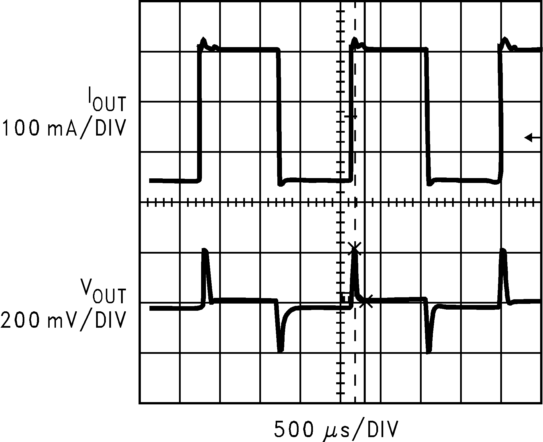
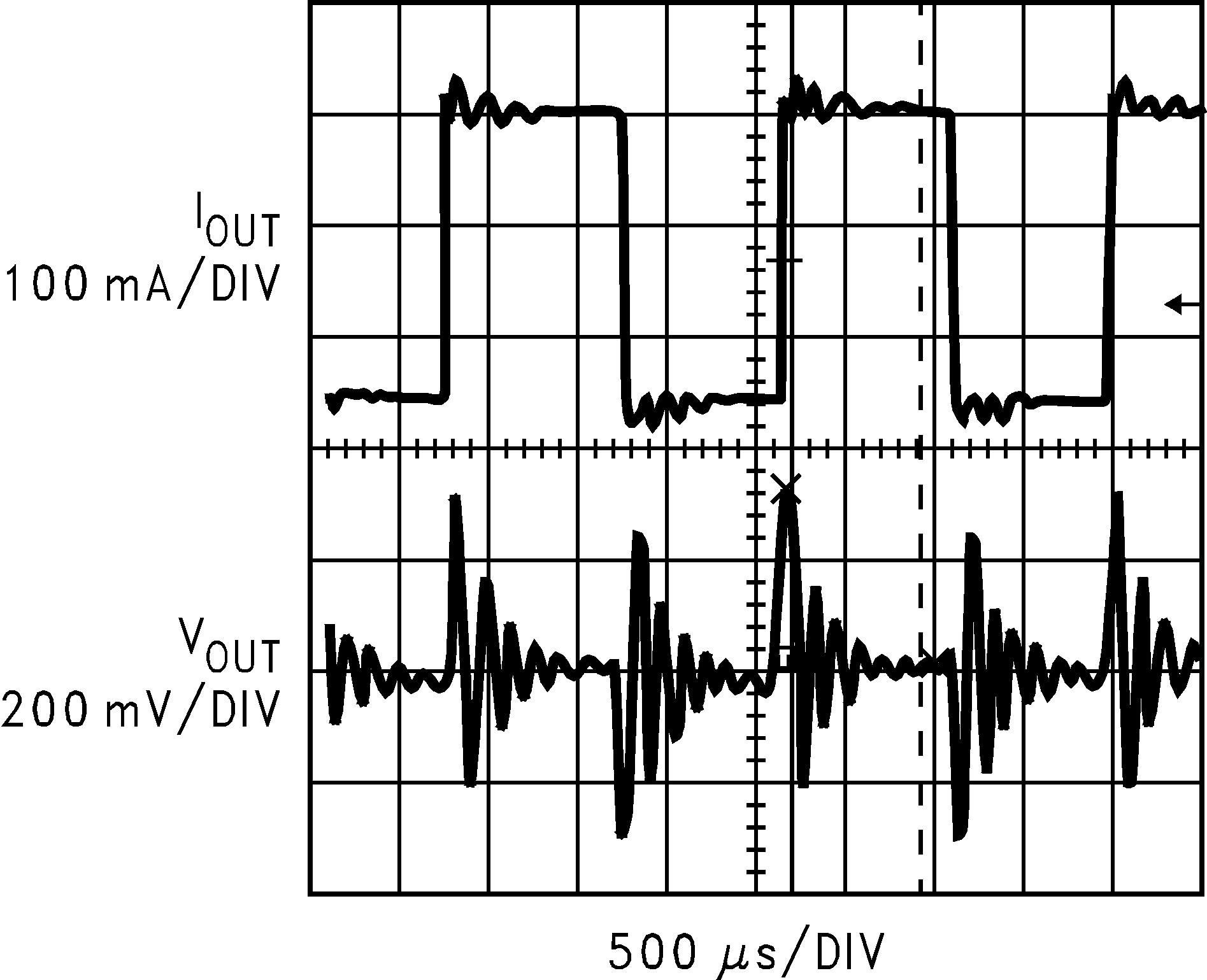
The compensator in the LM2611 is internal. However, a zero-pole pair can be added to the open-loop frequency response by inserting a feed-forward capacitor, CFF, in parallel to the top feedback resistor (RFB1). Phase margin and bandwidth can be improved with the added zero-pole pair. This in turn improves the transient response to a step load change (see Figure 17 and Figure 18). The position of the zero-pole pair is a function of the feedback resistors and the capacitor value:


The optimal position for this zero-pole pair will vary with circuit parameters such as D, IOUT, COUT, L1, L2, and CCUK. For most cases, the value for the zero frequency is between 5 kHz to 20 kHz. Notice how the pole position, ωp, is dependant on the feedback resistors RFB1 and RFB2, and therefore also dependant on the output voltage. As the output voltage becomes closer to −1.26 V, the pole moves towards the zero, tending to cancel it out. If the absolute magnitude of the output voltage is less than 3.3 V, adding the zero-pole pair will not have much effect on the response.
7.4 Device Functional Modes
7.4.1 Hysteretic Mode
As the output current decreases, the energy stored in the Cuk capacitor eventually exceeds the energy required by the load. The excess energy is absorbed by the output capacitor, causing the output voltage to increase out of regulation. The LM2611 detects when this happens and enters a pulse-skipping, or hysteretic mode. In pulse-skipping mode, the output voltage increases as illustrated in Figure 20 as opposed to the regular PWM operation shown in Figure 19. Figure 19 shows the LM2611 in PWM Mode with very-low ripple. Figure 20 shows the LM2611 in pulse-skipping mode at low loads. In this mode, the output ripple increases slightly.
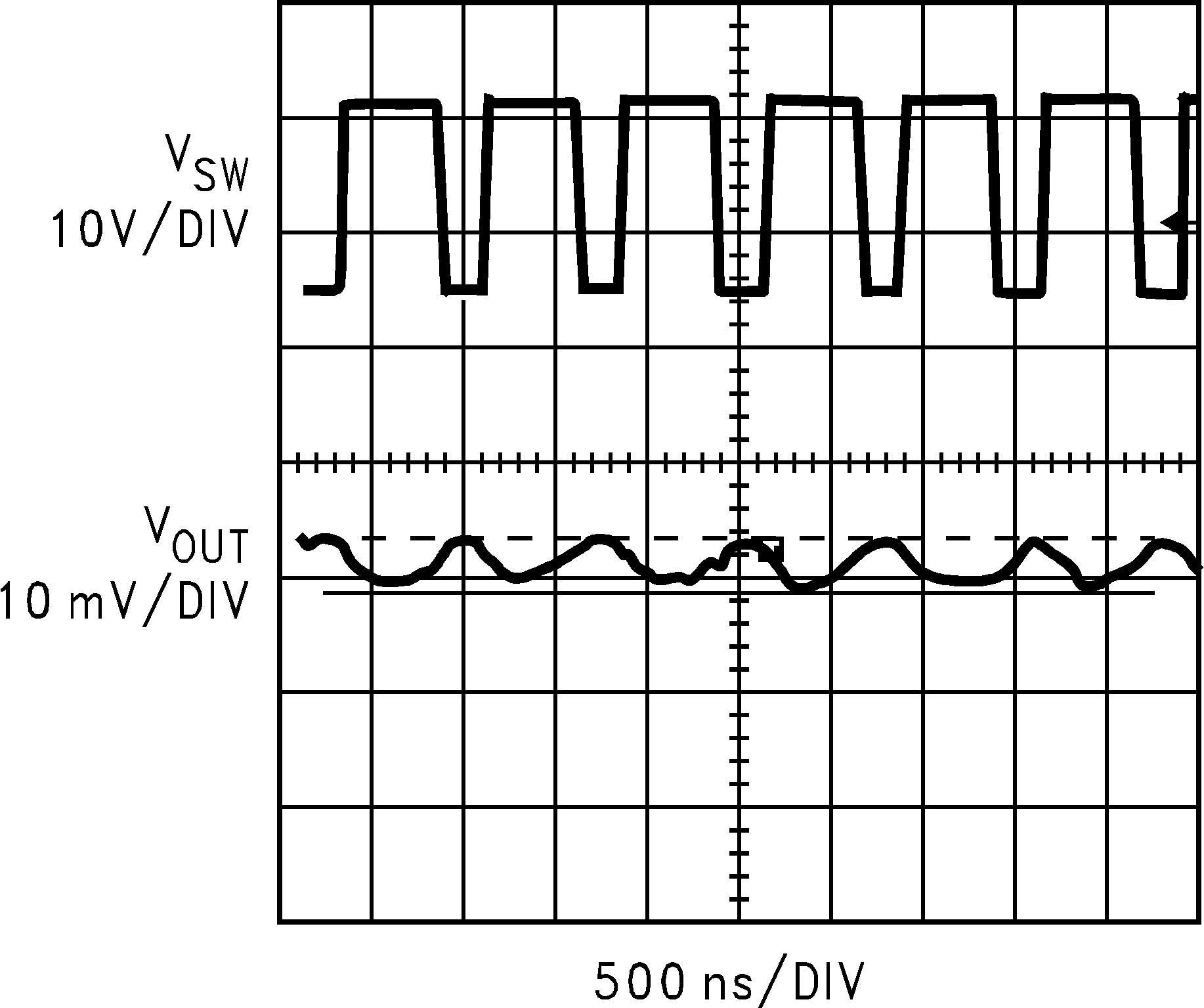 Figure 19. PWM Mode
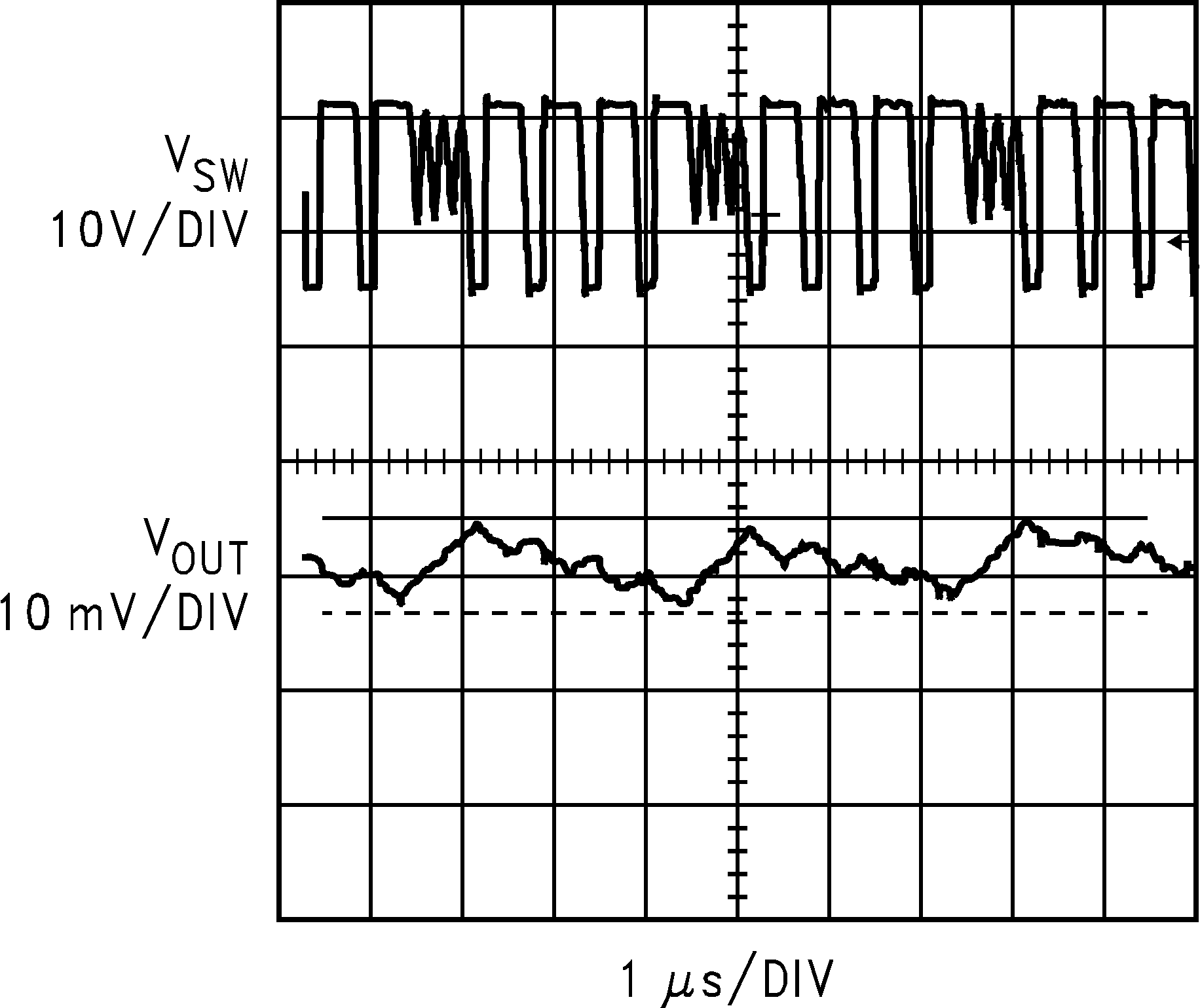 Figure 20. Pulse-Skipping Mode
7.4.1.1 Thermal Shutdown
If the junction temperature of the LM2611 exceeds 163°C, the device enters thermal shutdown. In thermal shutdown, the part deactivates the driver and the switch turns off. The switch remains off until the junction temperature drops to 155°C, at which point the part begins switching again. It will typically take 10 ms for the junction temperature to drop from 163°C to 155°C with the switch off.
