SNOSCS3B September 2013 – March 2014 LMP91300
PRODUCTION DATA.
- 1 Features
- 2 Applications
- 3 Description
- 4 Revision History
- 5 Terminal Configuration and Functions
- 6 Specifications
-
7 Detailed Description
- 7.1 Overview
- 7.2 Functional Block Diagram
- 7.3 Feature Description
- 7.4 Device Functional Modes
- 7.5 Programming
- 7.6
Register Maps
- 7.6.1 DET_H_MSB_INIT - Detection High Threshold MSB (Initial) (Address 0x66)
- 7.6.2 DET_H_LSB_INIT - Detection High Threshold LSB (Initial) (Address 0x67)
- 7.6.3 DET_L_MSB_INIT - Detection Low Threshold MSB (Initial) (Address 0x68)
- 7.6.4 DET_L_LSB_INIT - Detection Low Threshold LSB (Initial) (Address 0x69)
- 7.6.5 INFO0 - Device Information 0 (Address 0x6A)
- 7.6.6 INFO1 - Device Information 1 (Address 0x6B)
- 7.6.7 INFO2 - Device Information 2 (Address 0x6C)
- 7.6.8 INFO3 - Device Information 3 (Address 0x6D)
- 7.6.9 OSC_CONFIG_0 - Oscillator Configuration 0 Register (Address 0x6E)
- 7.6.10 45
- 7.6.11 OSC_CONFIG_1 - Oscillator Configuration 1 Register (Address 0x6F)
- 7.6.12 OSC_CONFIG_2 - Oscillator Configuration 2 Register (Address 0x70)
- 7.6.13 OSC_CONFIG_3_INIT - Oscillator Configuration 3 Register (Initial) (Address 0x71)
- 7.6.14 OUT_CONFIG_INIT - Output Configuration Register (Initial) (Address 0x72)
- 7.6.15 DET_H_MSB_FNL - Detection High Threshold MSB (Final) (Address 0x73)
- 7.6.16 DET_H_LSB_FNL - Detection High Threshold LSB (Final) (Address 0x74)
- 7.6.17 DET_L_MSB_FNL - Detection Low Threshold MSB (Final) (Address 0x75)
- 7.6.18 DET_L_LSB_FNL - Detection Low Threshold LSB (Final) (Address 0x76)
- 7.6.19 OSC_CONFIG_3_FNL - Oscillator Configuration 3 Register (Final) (Address 0x77)
- 7.6.20 OUT_CONFIG_FNL - Output Configuration Register (Final) (Address 0x78)
- 7.6.21 TEMP64 - Temperature In °C + 64 (Address 0x79)
- 7.6.22 PROXIMITY_MSB - Proximity MSB (Address 0x7A)
- 7.6.23 PROXIMITY_LSB - Proximity LSB (Address 0x7B)
- 7.6.24 STATUS - Device Status (Address 0x7E)
- 7.6.25 BURN_REQ - Burn Request (Address 0x7F)
-
8 Application and Implementation
- 8.1 Application Information
- 8.2
Typical Application
- 8.2.1 Design Requirements
- 8.2.2
Detailed Design Procedure
- 8.2.2.1 Quick Start
- 8.2.2.2 Determining The RP of an LC Tank
- 8.2.2.3 Component Selection And Layout
- 8.2.2.4 CF (CFA and CFB Terminals)
- 8.2.2.5 NTC (TEMP+ Terminal)
- 8.2.2.6 C1
- 8.2.2.7 CV+/EXT E
- 8.2.2.8 CBY (CBY Terminal)
- 8.2.2.9 RSENSE
- 8.2.2.10 REXT B (EXT B Terminal):
- 8.2.2.11 R1
- 8.2.2.12 SENSE1+ And SENSE2+ Terminals (RSENSE1+, RSENSE2+)
- 8.2.2.13 NPN
- 8.2.2.14 PNP
- 8.2.2.15 LED
- 8.2.2.16 LC Tank and INA and INB Terminals
- 8.2.2.17 SWDRV Terminal
- 8.2.2.18 P1 To P5 Terminals
- 8.2.2.19 GND Terminals
- 8.2.2.20 NC Terminals
- 8.2.2.21 Exposed DAP
- 8.2.2.22 SENSE-
- 8.2.3 Look-Up Table Calibration
- 9 Power Supply Recommendations
- 10Layout
- 11Device and Documentation Support
- 12Mechanical, Packaging, and Orderable Information
パッケージ・オプション
メカニカル・データ(パッケージ|ピン)
サーマルパッド・メカニカル・データ
発注情報
7 Detailed Description
7.1 Overview
The LMP91300 is a complete analog front end (AFE) optimized for use in inductive proximity sensors. The LMP91300 detects the presence of a metal object based on the RP change of an LC oscillator, depending on the distance of the metal object.
The LMP91300 is based on a novel architecture that directly converts the RP of the external LC tank to a digital value. Post manufacturing configuration and calibration is fully supported by the architecture of the LM91300. The temperature dependence of the sensor is digitally compensated, using an external temperature sensor. The LMP91300 provides programmable thresholds, programmable temperature compensation and programmable oscillation frequency range. Due to its programmability, the LMP91300 can be used with a wide variety of external inductors and its detection thresholds can be adjusted to the desired detection distances. The internal LDO has a high input voltage capability, while the architecture enables the use of a low supply as well. The output can be programmed to drive an external transistor in either NPN or PNP mode.
7.2 Functional Block Diagram
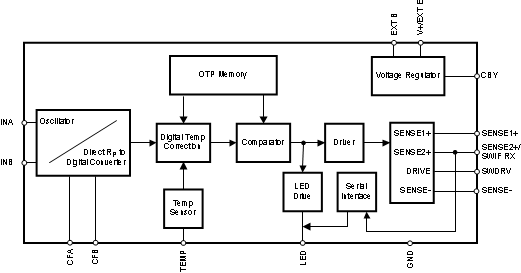
7.3 Feature Description
7.3.1 Oscillator
The oscillator, using an external LC tank (the detector), provides a wide oscillation range from 5kHz to 5MHz. The RP upper and lower limits are programmable, to support a wide range of LC combinations. Within the RP range of the LC tank, the oscillator amplitude is kept constant. When the LC tank RP drops below the lower programmed limit of RP the LMP91300 detects that the target is too close, the amplitude is reduced and the detector output will rail. See Figure 14.
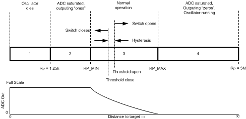 Figure 14. Operating Region
7.3.2 Detection
The RP of the external LC tank is directly converted to a digital signal. With this approach the only temperature compensation needed is that for RP, which is done through the Look Up Table (Registers 0x00 to 0x5D).
7.3.3 Comparator
The internal digital comparator accepts the signal from the RP to digital converter, after temperature compensation, and makes a decision, based on the value written to the DET_H_MSB and DET_H_ LSB registers. Programmable hysteresis is set by the value in the DET_L_MSB and DET_L_ LSB registers. The detection threshold can be set within the programmed RP range.
7.3.4 Low RP, Close Target, Under Range Switch Enable
If RP drops below the detectable range, the LMP91300 remains functional. The following applies if at least one temperature conversion has been completed:
For low RP start up (for example, if the target is in contact with the sensing coil when the part is powered on) UNDER_RANGE_SWITCH_EN must be set to 1 for the switch to be enabled. If UNDER_RANGE_SWITCH_EN is set to 0, the startup state is undefined when the sensor RP < RPMIN (for example, if the target is in contact with the sensing coil).
- If RP < 798Ω (for example, the metal plate is against the sensor) before the fourth conversion of the RP to digital converter (after Power On Reset) the switch will be activated regardless of the UNDER_RANGE_SWITCH_EN setting.
- If RP < 798Ω after the fourth conversion the switch state depends on the setting of UNDER_RANGE_SWITCH_EN.
- If UNDER_RANGE_SWITCH_EN = 1: The switch will be enabled.
- If UNDER_RANGE_SWITCH_EN = 0: The previous switch state will be held until the oscillation restarts (RP > 798Ω) and enough time has passed for a conversion to update the switch status.
If a temperature conversion has not been completed the switch state will not be changed.
The LMP91300 oscillator will begin to oscillate in less than 10 oscillator periods once the low RP condition is removed.
7.3.5 Programming The Switching Point And Hysteresis
The typical procedure is that the user puts a target metal at the target distance in front of the manufactured sensor system. The PROXIMITY_MSB and Proximity LSB registers are read and the DET_H_MSB and DET_H_ LSB registers are written with a value that causes the LMP91300 to switch. The metal target is then moved to another distance, farther away than the first distance, the PROXIMITY_MSB and Proximity LSB registers are read and a value is written to the DET_L_MSB and DET_L_ LSB registers that causes the LMP91300 to switch the external transistor off.
7.3.6 Temperature Compensation
As most of the integrated electronics are in the digital domain, close to perfect performance of the LMP91300 over temperature can be expected. As the RP factor of the external LC tank is measured, only the temperature coefficient of the LC tank losses need to be compensated for. The LMP91300 offers a digital temperature compensation feature that provides an accurate RP detection of the external LC tank when losses are introduced due to ambient temperature changes in the operating environment. This can be done by calibrating the Temperature Look-Up Table (LUT) located in registers 0x00 to 0x5D. The calibration involves the user generating gain correction factor coefficients (GCF) and is discussed in detail in the Look-Up Table Calibration section. These registers hold 2 bytes of information representing temperatures ranging from -48°C to 136°C in 4°C increments. The LMP91300 uses linear interpolation to provide 1°C temperature steps in between these 4°C points to improve accuracy. After the LUT has been properly programmed, the Detection Threshold registers need to be programmed for the switching distances desired. The external temperature sensor and the temperature coefficients stored in the LUT produce a functional temperature compensation system. The LUT was designed for an NTC with a beta factor β = 4250 such as the Murata NCP03WF104F05RL. Any other NTC used in the design will require additional adjustments which are explained in the Look-Up Table Calibration section.
7.3.7 Power Supply
An internal regulator with an external NPN transistor is used to power the LMP91300 directly from the loop.
7.3.8 LED Drive
An external LED can be driven with the LED terminal. Red and Green LEDs are supported. The LED current can be programmed to 2.5mA or 5 mA. This LED indicates the state of the sensor. Typically the LED is on if the switch is closed, but this is programmable in the OUT_CONFIG_INIT and OUT_CONFIG_FNL registers. This LED will also indicate an output overload condition situation or ECC error.
7.3.9 SWDRV
The LMP91300 drives an external transistor, to implement a NPN or PNP function. During power up the drive terminal (SWDRV) is pulled down using a high resistance to avoid turning on the external transistor, until the LMP91300 is fully functional.
7.3.10 Overload Protection
Short circuit detection and overload protection are implemented in the LMP91300, using an external SENSE resistor, RSENSE. When the voltage drop across RSENSE exceeds about 310 mV the LMP91300 detects a short circuit condition. If this condition persists, the switch is toggled between being open and closed. The switch will be on for about 30µs, with a duty cycle as set in OUT_CONFIG_INIT (0x72) bit 0 (SHORTCKT_DUTY_CYCLE) or OUT_CONFIG_FNL (0x78) bit 0 (SHORTCKT_DUTY_CYCLE) to protect the external BJT. For example, if SHORTCKT_DUTY_CYCLE is set to 0.1% the switch drive will be on for 30µs and off for 29.97ms (tOFF = (30µs/0.1%) - 30µs). During a short circuit event, the load current is limited to I=480mV/RSENSE. The LMP91300 will come out of the overload protection mode once the drop across RSENSE is less than 310mV.
When designing the overload protection circuitry the user must select the appropriate transistors, SWDRV current setting, RSENSE resistor and short circuit duty cycle. The transistor should be selected to handle the load current and supply voltage both during normal operation and during an overload situation to ensure that it remains in the safe operating region at all times. The RSENSE resistor should be chosen to set the current limit and over current threshold. The SWDRV current should be selected to ensure that during a short circuit condition the SWDRV current is capable of sourcing or sinking the programmed current depending on NPN or PNP configuration. This ensures that the short circuit control loop remains regulated and enforces the current limit and over current threshold. Once overload protection design is complete the user has the option to choose between the two duty cycle options.
7.4 Device Functional Modes
NPN and PNP 3 wire configurations as shown in the Typical Application section are supported by the LMP91300.
7.5 Programming
Through the 2-wire loop connection, all parameters such as the LUT, operation modes, output modes and detection thresholds can be programmed after the sensor manufacturing process is finished. The LMP91300 is one time programmable in a 3 step process. During the manufacturing process the configuration and calibration data will be written to the device and then a special code will be written that disables communication.
7.5.1 Burning Programmed Values Into The Registers
There are three steps to burning values into the registers.
- Burn the Temperature Look Up Table data (0x00 – 0x5D), initial registers, device information registers, and configuration registers (0x66 – 0x72).
- Use SWIF to program values into these registers (0x00 – 0x72).
- Use SWIF to write 0x08 to register 0x7F to permanently burn the values into the registers.
- Optional: Wait 300ms and read back the status register (0x7E). It should read 0x21 if the registers have been successfully burned.
- Burn final registers (0x73 – 0x78).
- Use SWIF to program values into these registers (0x73 – 0x78).
- Use SWIF to write 0x10 to register 0x7F to permanently burn the values into the registers.
- Optional: Wait 300ms and read back the status register (0x7E). It should read 0x23 if the registers have been successfully burned.
- Burn SWIF mode. After the device has been programmed the write function using SWIF needs to be disabled.
- Read Only. The SWIF write function is disabled but registers can still be read back using SWIF. Use SWIF to write 0x40 to address 0x7F. After the device is power cycled it will be read only.
- Disabled. The SWIF is completely disabled, both write and read functions are disabled. Use SWIF to write 0x80 to address 0x7F. After the device is power cycled SWIF will be disabled.
- Optional: Before power cycling the device wait 300ms and read back the status register (0x7E). It should read 0x27 for read only or 0x2F for SWIF disabled.
- 4. It is possible to combine steps 1 and 2 and burn the Look Up Table, initial registers, device information registers, configuration registers, and final registers (0x00 – 0x78) at one time.
- Use SWIF to program values into these registers (0x00 – 0x78).
- Use SWIF to write 0x20 to register 0x7F to permanently burn the values into the registers.
- Optional: Wait 300ms and read back the status register (0x7E). It should read 0x23 if the registers have been successfully burned.
7.5.2 Single-Wire Interface (SWIF)
The LMP91300 uses a bi-directional Single Wire Interface protocol to program and read registers. To communicate with the LMP91300 (slave) through the SWIF interface, the micro controller (master) must transmit (write) data through the DC loop supply voltage that should be set to +8V during programming or communication. This superimposed signal of pulses transitions between 8V and 12V is on top of the +8V DC loop supply voltage. When the master transmits data into the LMP91300 the signal propagates into the SENSE2+ terminal through the supply. The master receives data from the LMP91300 through the LED terminal in the form of alternating current pulses. These current pulses will be 5mA in amplitude. The LED terminal must be connected to ground, either through an LED or directly connected to ground for the LMP91300 to talk to the master.
The communication scheme utilizes various pulse width waveforms to represent different symbols as shown in Figure 15. The binary representation of a zero bit is represented by a 25% pulse duty cycle, a one bit is represented by a 75% pulse duty cycle, and idle bit is represented by a 50% duty cycle. All pulses transmitted must fall within the pulse width specifications provided within the electrical characteristics table.
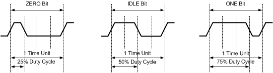 Figure 15. Single Wire Interface (SWIF) Symbol Diagram
The LMP91300 can be programmed at an input transfer bit rate between 1kbps to 10kbps. There is no acknowledge signal during the input data transfer so the master should read back the data to ensure data integrity and a successful data transfer has occurred. A read transaction is executed by the master transmitting data to configure the pointer register resulting in data output transfer by the slave. The LMP91300 transmits read back data at a speed of about 7kbps.
7.5.2.1 Write Operation
A frame begins with a minimum of one IDLE bit. To perform a write operation, the master must send an IDLE bit followed by the R/W bit set to 0 and the 7-bit address of the register that is intended to be programmed. The data to be written into the address location follows with the Most Significant Bit first and the write operation is terminated with an IDLE bit. There are 8 bits in each data byte and the maximum number of data bytes can be up to 8 bytes. Data being transmitted from the master to the slave can be terminated by the master by sending an IDLE bit after any data byte. After communication, to initiate another communication, the master must transmit another IDLE. When an invalid bit that violates the SWIF symbol protocol is transferred, the SWIF will reset and wait for the IDLE bit.
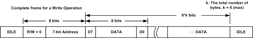 Figure 16. Complete Frame For A Write Command
7.5.2.2 Read Operation
The read signal is made by modulating the supply current. This can be read by using a SENSE resistor in the supply line. The LMP91300 modulates the supply current by sinking current into the LED terminal. The V+/EXT and LED terminals need to be connected by either an LED, resistor, or directly shorted for the Read operation to work. To perform a read operation, the master must send an IDLE bit to initiate communication, a R/W bit that should be set to 1, a 7-bit address, and another IDLE bit. Data is written back after the R/W and address byte are received so there must be a 9th rising edge to ensure that this condition is satisfied. After the last bit, A0, of the address is sent there should only be one rising edge to perform the IDLE bit. There are two valid methods of providing one rising edge, (1) a single pulse, or (2) a rising edge with the signal held high. See Figure 17 for a timing example of both cases.
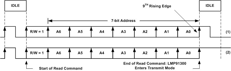 Figure 17. Read Timing Example: (1) Single Pulse, (2) Hold Signal High After Last Rising Edge
The LMP91300 goes into transmit mode 10μs plus a symbol length after the IDLE rising edge and no longer accepts any data until transmission is done. The master is not allowed to send anything until the slave has finished sending the data. Data is always written back on a read command with an IDLE bit, 8 bytes of data, and another IDLE bit. All transmitting is done in 8 byte blocks with the exception that only one byte is transmitted when the STATUS register (0x7E) is read. Since data transfer is always 8 bytes maximum (except for when register 0x7E, STATUS is read), there is a maximum wait time (8 bits*8 bytes + IDLE + IDLE + 10us) that the master must wait before taking ownership of the bus. The amount of time it takes for SWIF to switch from input to output is about one symbol.
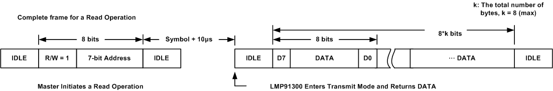 Figure 18. Complete Frame For A Read Command
The user has the option to set the LMP91300 into a read-only mode or SWIF disabled mode. When placed in read-only mode, the SWIF can only be used to read back the registers but all write capability is disabled. When placed in SWIF disabled mode, both read and write capabilities are disabled.
7.5.3 Usage Priority Of Registers
When a LMP91300 is powered on the register values that are used depends on if the LMP91300 has had values burned into the registers. See register 0x7F, BURN_REQ.
- No values have been burned into registers:
- When powered on the LMP91300 will use the default values in registers 0x00-0x5D and 0x66-0x72.
- If a value is written to any of these registers (0x00-0x5D and 0x66-0x72) the LMP91300 will use the value written instead of the power on default value.
- If a value is written into a FNL register (0x73-0x78) the LMP91300 will continue to use the value in the INIT register instead of the corresponding FNL register. For example, if register OSC_CONFIG_3_FNL (0x77) has a value written to it, the LMP91300 will continue using the OSC_CONFIG_3_INIT (0x71) register and not use the value in the OSC_CONFIG_3_FNL (0x77) register.
- If the LMP91300 is powered off and back on it will use the default values in registers 0x00-0x5D and 0x66-0x72.
- Values have been burned into the LMP91300 memory using burn request 0x08.
- When powered on the LMP91300 will use the burned values in registers 0x00-0x5D and 0x66-0x72.
- If a value is written to any of these registers (0x00-0x5D and 0x66-0x72) the LMP91300 will use the written value instead of the burned value.
- If a value is written into a FNL register (0x73-0x78) the LMP91300 will continue to use the value in the INIT register instead of the corresponding FNL register. For example, if register OSC_CONFIG_3_FNL (0x77) has a value written to it, the LMP91300 will continue using the OSC_CONFIG_3_INIT (0x71) register and not use the value in the OSC_CONFIG_3_FNL (0x77) register.
- If the LMP91300 is powered off and back on the LMP91300 will use the burned values in registers 0x00-0x5D and 0x66-0x72.
- Values have been burned into the LMP91300 memory using burn request 0x10 or 0x20.
- When powered on the LMP91300 will use the burned values in registers 0x00-0x5D, 0x6A-0x70 and 0x73-0x78.
- If a value is written to an INIT register (0x66-0x69, 0x71-0x72) it will be ignored and the corresponding FNL register (0x73-0x78) will be used.
- If a value is written to a FNL register (0x73-0x78) the LMP91300 will use the written value instead of the burned value.
- If the LMP91300 is powered off and then back on the LMP91300 will use the burned values in registers 0x00-0x5D, 0x6A-0x70 and 0x73-0x78.
It is important to remember that the LMP91300 will always use the values in the initial registers (either temporary written values or permanently burned values) if the final registers have not had values burned into them. If the final registers have had values burned into them, the LMP91300 will always use the final registers (either the permanently burned value or a value that has been temporally written in a final register).
The burn status of the LMP91300 can be determined by reading the STATUS register (0x7E) as long as a 0x80 burn request has not been issued.
Each register can only have a value burned into it one time. It is not possible to burn a value into a register multiple times.
7.6 Register Maps
| Name | Description | Address | Type | Default |
|---|---|---|---|---|
| LUT_x_GAIN_MSB, LSB | Temperature Look Up Table, -48°C to +136°C in 4°C steps, 2 bytes - gain | 0x00-0x5D | RW | 0x40 - even addresses, 0x00 - odd addresses |
| RESERVED | Reserved | 0x5E-0x65 | RO | 0x00 |
| DET_H_MSB_INIT | Detection High Threshold MSB (Initial) | 0x66 | RW | 0x00 |
| DET_H_LSB_INIT | Detection High Threshold LSB (Initial) | 0x67 | RW | 0x00 |
| DET_L_MSB_INIT | Detection Low Threshold MSB (Initial) | 0x68 | RW | 0x00 |
| DET_L_LSB_INIT | Detection Low Threshold LSB (Initial) | 0x69 | RW | 0x00 |
| INFO0 | Device Information 0 | 0x6A | RW | 0x00 |
| INFO1 | Device Information 1 | 0x6B | RW | 0x00 |
| INFO2 | Device Information 2 | 0x6C | RW | 0x00 |
| INFO3 | Device Information 3 | 0x6D | RW | 0x00 |
| OSC_CONFIG_0 | Oscillator Configuration 0 | 0x6E | RW | 0x0E |
| OSC_CONFIG_1 | Oscillator Configuration 1 | 0x6F | RW | 0x14 |
| OSC_CONFIG_2 | Oscillator Configuration 2 | 0x70 | RW | 0x45 |
| OSC_CONFIG_3_INIT | Oscillator Configuration 3 (Initial) | 0x71 | RW | 0x1B |
| OUT_CONFIG_INIT | Output Configuration (Initial) | 0x72 | RW | 0xA2 |
| DET_H_MSB_FNL | Detection High Threshold MSB (Final) | 0x73 | RW | 0x00 |
| DET_H_LSB_FNL | Detection High Threshold LSB (Final) | 0x74 | RW | 0x00 |
| DET_L_MSB_ FNL | Detection Low Threshold MSB (Final) | 0x75 | RW | 0x00 |
| DET_L_ LSB_ FNL | Detection Low Threshold LSB (Final) | 0x76 | RW | 0x00 |
| OSC_CONFIG_3_FNL | Oscillator Configuration 3 (Final) | 0x77 | RW | 0x1B |
| OUT_CONFIG_FNL | Output Configuration (Final) | 0x78 | RW | 0xA2 |
| TEMP64 | Temperature in °C + 64 | 0x79 | RO | NA |
| PROXIMITY_MSB | Proximity MSB | 0x7A | RO | NA |
| PROXIMITY_LSB | Proximity LSB | 0x7B | RO | NA |
| RESERVED | Reserved | 0x7C-0x7D | RO | 0x00 |
| STATUS | Device Status | 0x7E | RO | NA |
| BURN_REQ | Burn Request | 0x7F | WO | NA |
7.6.1 DET_H_MSB_INIT – Detection High Threshold MSB (Initial) (Address 0x66)
| Bit | Name | Function (Default values in bold) |
|---|---|---|
| [7:0] | DET_H_MSB_INIT | 0x00: Detection High Threshold MSB (Initial) |
See the Usage Priority Of Registers section.
A starting value to put in the DET_H_MSB_INIT and DET_H_LSB_INIT registers can be determined by first setting the correct values in the OSC_CONFIG_0, OSC_CONFIG_1, OSC_CONFIG_2, OSC_CONFIG_3_INIT, OUT_CONFIG_INIT registers, putting the target at the distance away from the target that it is supposed to switch on at, reading the values in the PROXIMITY_MSB and Proximity LSB registers, and writing these values into the DET_H_MSB_INIT and DET_H_LSB_INIT registers. This value can be then adjusted as needed.
7.6.2 DET_H_LSB_INIT – Detection High Threshold LSB (Initial) (Address 0x67)
| Bit | Name | Function (Default values in bold) |
|---|---|---|
| [7:0] | DET_H_LSB_INIT | 0x00: Detection High Threshold LSB (Initial) |
See the Usage Priority Of Registers section.
7.6.3 DET_L_MSB_INIT – Detection Low Threshold MSB (Initial) (Address 0x68)
| Bit | Name | Function (Default values in bold) |
|---|---|---|
| [7:0] | DET_L_MSB_INIT | 0x00: Detection Low Threshold MSB (Initial) |
See the Usage Priority Of Registers section.
A starting value to put in the DET_L_MSB_INIT and DET_L_LSB_INIT registers can be determined by first setting the correct values in the OSC_CONFIG_0, OSC_CONFIG_1, OSC_CONFIG_2, OSC_CONFIG_3_INIT, OUT_CONFIG_INIT registers, putting the target at the distance away from the target that it is supposed to switch off at, reading the values in the PROXIMITY_MSB and Proximity LSB registers, and writing these values into the DET_L_MSB_INIT and DET_L_LSB_INIT registers. This value can be then adjusted as needed.
7.6.4 DET_L_LSB_INIT – Detection Low Threshold LSB (Initial) (Address 0x69)
| Bit | Name | Function (Default values in bold) |
|---|---|---|
| [7:0] | DET_L_LSB_INIT | 0x00: Detection Low Threshold LSB (Initial) |
See the Usage Priority Of Registers section.
7.6.5 INFO0 – Device Information 0 (Address 0x6A)
| Bit | Name | Function (Default values in bold) |
|---|---|---|
| [7:0] | INFO0 | 0x00: Device Information 0 |
This register can be used to store information such as assembly date, model number, revision number or any other data.
7.6.6 INFO1 – Device Information 1 (Address 0x6B)
| Bit | Name | Function (Default values in bold) |
|---|---|---|
| [7:0] | INFO1 | 0x00: Device Information 1 |
This register can be used to store information such as assembly date, model number, revision number or any other data.
7.6.7 INFO2 – Device Information 2 (Address 0x6C)
| Bit | Name | Function (Default values in bold) |
|---|---|---|
| [7:0] | INFO2 | 0x00: Device Information 2 |
This register can be used to store information such as assembly date, model number, revision number or any other data.
7.6.8 INFO3 – Device Information 3 (Address 0x6D)
| Bit | Name | Function (Default values in bold) |
|---|---|---|
| [7:0] | INFO3 | 0x00: Device Information 3 |
This register can be used to store information such as assembly date, model number, revision number or any other data.
7.6.9 OSC_CONFIG_0 – Oscillator Configuration 0 Register (Address 0x6E)
| Bit | Name | Function (Default values in bold) |
|---|---|---|
| [7:5] | Reserved | 000 |
| [4:0] | RP_MAX | 01110: Maximum RP, logarithmic scale |
The optimal setting for RP_MAX is the highest value for which the correct amplitude is maintained, with the target set at the maximum switching distance.
- Determine RLCTANK as shown in the Determining The RP of an LC Tank section.
- Multiply RPLCTANK by 2 and use the next higher value from the chart below. For example, if RPLCTANK measured at 4mm is 11113, 11113x2 = 22226, so 12 (27704) would be used for RP_MAX.
- This value can be adjusted up or down as needed.
7.6.10
| Register Setting (Hex) | RP (Ω) | Register Setting (Hex) | RP (Ω) | Register Setting (Hex) | RP (Ω) | ||
|---|---|---|---|---|---|---|---|
| 0 | 3926991 | B | 193926 | 16 | 9235 | ||
| 1 | 3141593 | C | 145444 | 17 | 7182 | ||
| 2 | 2243995 | D | 109083 | 18 | 5387 | ||
| 3 | 1745329 | E | 83111 | 19 | 4309 | ||
| 4 | 1308997 | F | 64642 | 1A | 3078 | ||
| 5 | 981748 | 10 | 48481 | 1B | 2394 | ||
| 6 | 747998 | 11 | 38785 | 1C | 1796 | ||
| 7 | 581776 | 12 | 27704 | 1D | 1347 | ||
| 8 | 436332 | 13 | 21547 | 1E | 1026 | ||
| 9 | 349066 | 14 | 16160 | 1F | 798 | ||
| A | 249333 | 15 | 12120 |
7.6.11 OSC_CONFIG_1 – Oscillator Configuration 1 Register (Address 0x6F)
| Bit | Name | Function (Default values in bold) |
|---|---|---|
| [7:5] | PADC_TIMEC | 000: Sensor time constant range |
| [4:0] | RP_MIN | 10100: Minimum RP, logarithmic scale |
The PADC_TIMEC (time constant), sets the damping of the readout circuitry. The higher this Parameter is set, the more damping it has. If programmed to zero (0), it has no damping, and the system is almost unstable. The oscillation amplitude (envelope) will vary a lot. If this parameter is set to max (7), the damping is maximum, but that also means the response becomes slow. The optimal setting is what in control theory is called "critical damping", that is the least damping required to prevent overshoot in the step response. In most cases set PADC_TIMEC = 1.
The optimal setting for RP_MIN is the highest value for which the correct amplitude is maintained, with the target at the minimum switching distance. Some margin is given to the value.
- Determine RPLCTANK as shown in the Determining The RP of an LC Tank section.
- Divide the RPLCTANK value by 2 and then select the next lower RP value from the chart above. For example, if the finished Proximity Sensor is to detect at 4mm and the RPLCTANK measured at 4mm is 11113, 11113/2 = 5556.5, so 18 (5387) would be used for RP_MIN.
- This value can be adjusted up or down as needed.
7.6.12 OSC_CONFIG_2 – Oscillator Configuration 2 Register (Address 0x70)
| Bit | Name | Function (Default values in bold) |
|---|---|---|
| [7:0] | RESONATOR_MIN_FREQ | 01000101: Minimum frequency setting, logarithmic scale |
Determine the minimum oscillation frequency (fMIN) of the LC tank. This is when there is no target in front of the LC tank. Calculate a value 20% below the minimum oscillation frequency, f80% = fMIN x 0.8. Use the following formula to calculate the value for RESONATOR_MIN_FREQ:

Take this value, round up to the next integer and convert to hex.
7.6.13 OSC_CONFIG_3_INIT – Oscillator Configuration 3 Register (Initial) (Address 0x71)
| Bit | Name | Function (Default values in bold) |
|---|---|---|
| [7:6] | RESERVED | 00 |
| [5] | UNDER_RANGE_SWITCH_EN | 0: Off 1: On |
| [4:3] | OSC_AMP | 00: 1V 01: 2V 10: 4V 11: Reserved |
| [2:0] | RESPONSE_TIME | 000: Reserved 001: 96 010: 192 011: 384 100: 768 101: 1536 110: 3072 111: 6144 |
See the Usage Priority Of Registers section.
UNDER_RANGE_SWITCH_EN: The following applies if at least one temperature conversion has been completed:
- If RP < 798Ω (for example, the metal plate is against the sensor) before the fourth conversion of the RP to digital converter (after Power On Reset) the switch will be activated regardless of the UNDER_RANGE_SWITCH_EN setting.
- If RP < 798Ω after the fourth conversion the switch state depends on the setting of UNDER_RANGE_SWITCH_EN.
- If UNDER_RANGE_SWITCH_EN = 1: The switch will be enabled.
- If UNDER_RANGE_SWITCH_EN = 0: The previous switch state will be held until the oscillation restarts (RP > 798Ω) and enough time has passed for a conversion to update the switch status.
If a temperature conversion has not been completed the switch state will not be changed.
OSC_AMP: The oscillation amplitude at terminals INA and INB can be set to 1V, 2V, or 4V. If the LMP91300 has not been burned with user values, the power on value for OSC_AMP is 11: Reserved. This will need to be changed to either 1V, 2V or 4V before the LMP91300 is used.
RESPONSE_TIME: Using a lower response time will shorten the settling time of the digital filter and give faster readings from the RP to digital converter but will increase the noise in the reading. A higher setting gives the digital filter more time to settle and will decrease the noise in the reading.
7.6.14 OUT_CONFIG_INIT – Output Configuration Register (Initial) (Address 0x72)
| Bit | Name | Function (Default values in bold) |
|---|---|---|
| [7:6] | SWDRV_CURRENT | 00: 2.5mA 01: 3.75mA 10: 5mA 11: 10mA |
| 5 | OUTPUT_MODE | 0: 3-Wire NPN 1: 3-Wire PNP |
| 4 | DRIVE_MODE | 0: Normally open 1: Normally closed |
| 3 | LED_ENABLE | 0: On 1: Off |
| 2 | LED_MODE | 0: Normally off 1: Normally on |
| 1 | LED_CURRENT | 0: 2.5mA 1: 5mA |
| 0 | SHORTCKT_DUTY_CYCLE | 0: 0.1% 1: 0.8% |
See the Usage Priority Of Registers section.
SWDRV_CURRENT: Used to set the amplitude of current from the SWDRV terminal used to control the external transistor.
DRIVE_MODE: Normally open and normally closed refer to the external NPN or PNP switch when a target is far away from the inductive sensor. When the switch is normally open the transistor is not conducting when the target is far away from the target (the distance is greater than the value in DET_L_MSB and DET_L_ LSB). The switch is conducting when the target is close to the sensor (the distance is less than the value in DET_H_MSB and DET_H_ LSB). When the switch is normally closed the transistor is conducting when the target is far away from the target (the distance is greater than the value in DET_L_MSB and DET_L_ LSB). The switch is not conducting when the target is close to the sensor (the distance is less than the value in DET_H_MSB and DET_H_ LSB).
LED_ENABLE: When set to On the LED will function as set in Bit 2, LED_MODE. When set to Off the LED will always be off.
LED_MODE: Normally off means that the LED is off when the target is far away from the sensor (the distance is greater than the value in DET_L_MSB and DET_L_ LSB). The LED will turn on when the target is close (the distance is less than the value in DET_H_MSB and DET_H_ LSB). Normally on means that the LED is on when the target is far away from the sensor (the distance is greater than the value in DET_L_MSB and DET_L_ LSB). ). The LED will turn off when the target is close (the distance is less than the value in DET_H_MSB and DET_H_ LSB).
LED_CURRENT: Sets the current through the LED.
SHORTCKT_DUTY_CYCLE: When the LMP91300 is in overload protection mode it will test to determine if the overload condition is still present. The switch will be on for about 30µs, with an on to off duty cycle as set by SHORTCKT_DUTY_CYCLE to protect the external BJT. For example, if SHORTCKT_DUTY_CYCLE is set to 0.1% the switch drive will be on for 30µs and off for 29.97ms (tOFF = (30µs/0.1%) - 30µs).
7.6.15 DET_H_MSB_FNL – Detection High Threshold MSB (Final) (Address 0x73)
| Bit | Name | Function (Default values in bold) |
|---|---|---|
| [7:0] | DET_H_MSB_FNL | 0x00: Detection High Threshold MSB (Final) |
See the Usage Priority Of Registers section.
A starting value to put in the DET_H_MSB_FNL and DET_H_LSB_FNL registers can be determined by first setting the correct values in the OSC_CONFIG_0, OSC_CONFIG_1, OSC_CONFIG_2, OSC_CONFIG_3_INIT/FNL, OUT_CONFIG_INIT/FNL registers, putting the target at the distance away from the target that it is supposed to switch on at, reading the values in the PROXIMITY_MSB and Proximity LSB registers, and writing these values into the DET_H_MSB_INIT/FNL and DET_H_LSB_INIT/FNL registers. This value can be then adjusted as needed.
7.6.16 DET_H_LSB_FNL – Detection High Threshold LSB (Final) (Address 0x74)
| Bit | Name | Function (Default values in bold) |
|---|---|---|
| [7:0] | DET_H_LSB_FNL | 0x00: Detection High Threshold LSB (Final) |
See the Usage Priority Of Registers section.
7.6.17 DET_L_MSB_FNL – Detection Low Threshold MSB (Final) (Address 0x75)
| Bit | Name | Function (Default values in bold) |
|---|---|---|
| [7:0] | DET_L_MSB_FNL | 0x00: Detection Low Threshold MSB (Final) |
See the Usage Priority Of Registers section.
A starting value to put in the DET_L_MSB_FNL and DET_L_LSB_FNL registers can be determined by first setting the correct values in the OSC_CONFIG_0, OSC_CONFIG_1, OSC_CONFIG_2, OSC_CONFIG_3_INIT/FNL, OUT_CONFIG_INIT/FNL registers, putting the target at the distance away from the target that it is supposed to switch off at, reading the values in the PROXIMITY_MSB and Proximity LSB registers, and writing these values into the DET_L_MSB_INIT/FNL and DET_L_LSB_INIT/FNL registers. This value can be then adjusted as needed.
7.6.18 DET_L_LSB_FNL – Detection Low Threshold LSB (Final) (Address 0x76)
| Bit | Name | Function (Default values in bold) |
|---|---|---|
| [7:0] | DET_L_LSB_FNL | 0x00: Detection Low Threshold LSB (Final) |
See the Usage Priority Of Registers section.
7.6.19 OSC_CONFIG_3_FNL – Oscillator Configuration 3 Register (Final) (Address 0x77)
| Bit | Name | Function (Default values in bold) |
|---|---|---|
| [7:6] | RESERVED | 00 |
| [5] | UNDER_RANGE_SWITCH_EN | 0: Off 1: On |
| [4:3] | OSC_AMP | 00: 1V 01: 2V 10: 4V 11: Reserved |
| [2:0] | RESPONSE_TIME | 000: Reserved 001: 96 010: 192 011: 384 100: 768 101: 1536 110: 3072 111: 6144 |
See the Usage Priority Of Registers section.
UNDER_RANGE_SWITCH_EN: The following applies if at least one temperature conversion has been completed:
- If RP < 798Ω (for example, the metal plate is against the sensor) before the fourth conversion of the RP to digital converter (after Power On Reset) the switch will be activated regardless of the UNDER_RANGE_SWITCH_EN setting.
- If RP < 798Ω after the fourth conversion the switch state depends on the setting of UNDER_RANGE_SWITCH_EN.
- If UNDER_RANGE_SWITCH_EN = 1: The switch will be enabled.
- If UNDER_RANGE_SWITCH_EN = 0: The previous switch state will be held until the oscillation restarts (RP > 798Ω) and enough time has passed for a conversion to update the switch status.
If a temperature conversion has not been completed the switch state will not be changed.
OSC_AMP: The oscillation amplitude at terminals INA and INB can be set to 1V, 2V, or 4V. If the LMP91300 has not been burned with user values, the power on value for OSC_AMP is 11: Reserved. This will need to be changed to either 1V, 2V or 4V before the LMP91300 is used.
RESPONSE_TIME: Using a lower response time will shorten the settling time of the digital filter and give faster readings from the RP to digital converter but will increase the noise in the reading. A higher setting gives the digital filter more time to settle and will decrease the noise in the reading.
7.6.20 OUT_CONFIG_FNL – Output Configuration Register (Final) (Address 0x78)
| Bit | Name | Function (Default values in bold) |
|---|---|---|
| [7:6] | SWDRV_CURRENT | 00: 2.5mA 01: 3.75mA 10: 5mA 11: 10mA |
| 5 | OUTPUT_MODE | 0: 3-Wire NPN 1: 3-Wire PNP |
| 4 | DRIVE_MODE | 0: Normally open 1: Normally closed |
| 3 | LED_ENABLE | 0: On 1: Off |
| 2 | LED_MODE | 0: Normally off 1: Normally on |
| 1 | LED_CURRENT | 0: 2.5mA 1: 5mA |
| 0 | SHORTCKT_DUTY_CYCLE | 0: 0.1% 1: 0.8% |
See the Usage Priority Of Registers section.
SWDRV_CURRENT: Used to set the amplitude of current from the SWDRV terminal used to control the external transistor.
DRIVE_MODE: Normally open and normally closed refer to the external NPN or PNP switch when a target is far away from the inductive sensor. When the switch is normally open the transistor is not conducting when the target is far away from the target (the distance is greater than the value in DET_L_MSB and DET_L_ LSB). The switch is conducting when the target is close to the sensor (the distance is less than the value in DET_H_MSB and DET_H_ LSB). When the switch is normally closed the transistor is conducting when the target is far away from the target (the distance is greater than the value in DET_L_MSB and DET_L_ LSB). The switch is not conducting when the target is close to the sensor (the distance is less than the value in DET_H_MSB and DET_H_ LSB).
LED_ENABLE: When set to On the LED will function as set in Bit 2, LED_MODE. When set to Off the LED will always be off.
LED_MODE: Normally off means that the LED is off when the target is far away from the sensor (the distance is greater than the value in DET_L_MSB and DET_L_ LSB). The LED will turn on when the target is close (the distance is less than the value in DET_H_MSB and DET_H_ LSB). Normally on means that the LED is on when the target is far away from the sensor (the distance is greater than the value in DET_L_MSB and DET_L_ LSB). ). The LED will turn off when the target is close (the distance is less than the value in DET_H_MSB and DET_H_ LSB).
LED_CURRENT: Sets the current through the LED.
SHORTCKT_DUTY_CYCLE: When the LMP91300 is in overload protection mode it will test to determine if the overload condition is still present. The switch will be on for about 30µs, with an on to off duty cycle as set by SHORTCKT_DUTY_CYCLE to protect the external BJT. For example, if SHORTCKT_DUTY_CYCLE is set to 0.1% the switch drive will be on for 30µs and off for 29.97ms (tOFF = (30µs/0.1%) - 30µs).
7.6.21 TEMP64 – Temperature In °C + 64 (Address 0x79)
| Bit | Name | Function (Default values in bold) |
|---|---|---|
| [7:0] | TEMP64 | Temperature in °C + 64 |
Convert the value read from this register to decimal and subtract 64 to determine the temperature in °C.
7.6.22 PROXIMITY_MSB – Proximity MSB (Address 0x7A)
| Bit | Name | Function (Default values in bold) |
|---|---|---|
| [7:0] | PROXIMITY_MSB | Proximity MSB |
When a command is issued to read the PROXIMITY_MSB register, values from the RP to Digital converter are placed in the PROXIMITY_MSB and Proximity LSB registers. The value in the Proximity LSB register will not change until another read command of PROXIMITY_MSB is given. It is recommended that both the PROXIMITY_MSB and Proximity LSB registers be read together.
7.6.23 PROXIMITY_LSB – Proximity LSB (Address 0x7B)
| Bit | Name | Function (Default values in bold) |
|---|---|---|
| [7:0] | Proximity LSB | Proximity LSB |
7.6.24 STATUS – Device Status (Address 0x7E)
| Bit | Name | Function (Default values in bold) |
|---|---|---|
| 7 | PADC_TIMEOUT | 0: No timeout 1: Timeout |
| 6 | ECC_ERR | 0: No error 1: Error |
| 5 | BUSY | 0: Part is busy 1: Part is not busy |
| 4 | BURN_PROG | 0: No burn in progress 1: Burn in progress |
| [3:0] | SWIF_STATUS | 0x0: No burn has occurred, full SWIF access 0x1: Addresses 0x00 to 0x72 burned, full SWIF access 0x3: Addresses 0x00 to 0x78 burned, full SWIF access 0x7: Addresses 0x00 to 0x78 burned, SWIF is read only 0xF: Addresses 0x00 to 0x78 burned, SWIF is disabled |
When register 0x7E is read only one byte of data is transmitted from the LMP91300.
7.6.25 BURN_REQ – Burn Request (Address 0x7F)
| Bit | Name | Function (Default values in bold) |
|---|---|---|
| [7:0] | BURN_REQ | 0x08: Burn Temperature Look Up Table data (0x00 – 0x5D), initial registers, device information registers, and configuration registers (0x66 – 0x72). 0x10: Burn final registers (0x73 – 0x78). 0x20: Burn all registers (0x00 – 0x78). 0x40: Set SWIF to read back mode. 0x80: Disable SWIF. |