SLVSCN6A November 2014 – December 2014 MSP430FR5739-EP
PRODUCTION DATA.
- 1Device Overview
- 2Revision History
- 3Pin Configuration and Functions
-
4Specifications
- 4.1 Absolute Maximum Ratings
- 4.2 Recommended Operating Conditions
- 4.3 Thermal Information
- 4.4 Active Mode Supply Current Into VCC Excluding External Current
- 4.5 Low-Power Mode Supply Currents (Into VCC) Excluding External Current
- 4.6 Schmitt-Trigger Inputs - General Purpose I/O (P1.0 to P1.7, P2.0 to P2.7, P3.0 to P3.7, P4.0 to P4.1, PJ.0 to PJ.5, RST/NMI)
- 4.7 Inputs - Ports P1 and P2 (P1.0 to P1.7, P2.0 to P2.7)
- 4.8 Leakage Current - General Purpose I/O (P1.0 to P1.7, P2.0 to P2.7, P3.0 to P3.7, P4.0 to P4.1, PJ.0 to PJ.5, RST/NMI)
- 4.9 Outputs - General Purpose I/O (P1.0 to P1.7, P2.0 to P2.7, P3.0 to P3.7, P4.0 to P4.1, PJ.0 to PJ.5)
- 4.10 Output Frequency - General Purpose I/O (P1.0 to P1.7, P2.0 to P2.7, P3.0 to P3.7, P4.0 to P4.1, PJ.0 to PJ.5)
- 4.11 Typical Characteristics - Outputs
- 4.12 Crystal Oscillator, XT1, Low-Frequency (LF) Mode
- 4.13 Crystal Oscillator, XT1, High-Frequency (HF) Mode
- 4.14 Internal Very-Low-Power Low-Frequency Oscillator (VLO)
- 4.15 DCO Frequencies
- 4.16 MODOSC
- 4.17 PMM, Core Voltage
- 4.18 PMM, SVS, BOR
- 4.19 Wake-Up from Low Power Modes
- 4.20 Timer_A
- 4.21 Timer_B
- 4.22 eUSCI (UART Mode) Recommended Operating Conditions
- 4.23 eUSCI (UART Mode)
- 4.24 eUSCI (SPI Master Mode) Recommended Operating Conditions
- 4.25 eUSCI (SPI Master Mode)
- 4.26 eUSCI (SPI Slave Mode)
- 4.27 eUSCI (I2C Mode)
- 4.28 10-Bit ADC, Power Supply and Input Range Conditions
- 4.29 10-Bit ADC, Timing Parameters
- 4.30 10-Bit ADC, Linearity Parameters
- 4.31 REF, External Reference
- 4.32 REF, Built-In Reference
- 4.33 REF, Temperature Sensor and Built-In VMID
- 4.34 Comparator_D
- 4.35 FRAM
- 4.36 JTAG and Spy-Bi-Wire Interface
-
5Detailed Description
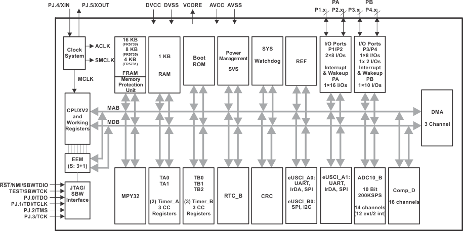
- 5.1 Functional Block Diagram
- 5.2 CPU
- 5.3 Operating Modes
- 5.4 Interrupt Vector Addresses
- 5.5 Memory Organization
- 5.6 Bootstrap Loader (BSL)
- 5.7 JTAG Operation
- 5.8 FRAM
- 5.9 Memory Protection Unit (MPU)
- 5.10
Peripherals
- 5.10.1 Digital I/O
- 5.10.2 Oscillator and Clock System (CS)
- 5.10.3 Power Management Module (PMM)
- 5.10.4 Hardware Multiplier (MPY)
- 5.10.5 Real-Time Clock (RTC_B)
- 5.10.6 Watchdog Timer (WDT_A)
- 5.10.7 System Module (SYS)
- 5.10.8 DMA Controller
- 5.10.9 Enhanced Universal Serial Communication Interface (eUSCI)
- 5.10.10 TA0, TA1
- 5.10.11 TB0, TB1, TB2
- 5.10.12 ADC10_B
- 5.10.13 Comparator_D
- 5.10.14 CRC16
- 5.10.15 Shared Reference (REF)
- 5.10.16 Embedded Emulation Module (EEM)
- 5.10.17 Peripheral File Map
-
6Input/Output Schematics
- 6.1 Port P1, P1.0 to P1.2, Input/Output With Schmitt Trigger
- 6.2 Port P1, P1.3 to P1.5, Input/Output With Schmitt Trigger
- 6.3 Port P1, P1.6 to P1.7, Input/Output With Schmitt Trigger
- 6.4 Port P2, P2.0 to P2.2, Input/Output With Schmitt Trigger
- 6.5 Port P2, P2.3 to P2.4, Input/Output With Schmitt Trigger
- 6.6 Port P2, P2.5 to P2.6, Input/Output With Schmitt Trigger
- 6.7 Port P2, P2.7, Input/Output With Schmitt Trigger
- 6.8 Port P3, P3.0 to P3.3, Input/Output With Schmitt Trigger
- 6.9 Port P3, P3.4 to P3.6, Input/Output With Schmitt Trigger
- 6.10 Port P3, P3.7, Input/Output With Schmitt Trigger
- 6.11 Port P4, P4.0, Input/Output With Schmitt Trigger
- 6.12 Port P4, P4.1, Input/Output With Schmitt Trigger
- 6.13 Port J, J.0 to J.3 JTAG pins TDO, TMS, TCK, TDI/TCLK, Input/Output With Schmitt Trigger or Output
- 6.14 Port PJ, PJ.4 and PJ.5 Input/Output With Schmitt Trigger
- 7Device Descriptors (TLV)
-
8Device and Documentation Support
- 8.1 Device Support
- 8.2 Documentation Support
- 8.3 Community Resources
- 8.4 Trademarks
- 8.5 Electrostatic Discharge Caution
- 8.6 Glossary
- 9Mechanical Packaging and Orderable Information
パッケージ・オプション
メカニカル・データ(パッケージ|ピン)
- RHA|40
サーマルパッド・メカニカル・データ
- RHA|40
発注情報
1 Device Overview
1.1 Features
- Embedded Microcontroller
- 16-Bit RISC Architecture up to 24-MHz Clock
- Wide Supply Voltage Range (2 to 3.6 V)
- –55°C to 85°C Operation
- Optimized Ultra-Low-Power Modes
- Active Mode: 81.4 µA/MHz (Typical)
- Standby (LPM3 With VLO): 6.3 µA (Typical)
- Real-Time Clock (LPM3.5 With Crystal): 1.5 µA (Typical)
- Shutdown (LPM4.5): 0.32 µA (Typical)
- Ultra-Low-Power Ferroelectric RAM (FRAM)
- Up to 16KB of Nonvolatile Memory
- Ultra-Low-Power Writes
- Fast Write at 125 ns per Word (16KB in 1 ms)
- Built-In Error Correction Coding (ECC) and Memory Protection Unit (MPU)
- Universal Memory = Program + Data + Storage
- 1015 Write Cycle Endurance
- Radiation Resistant and Nonmagnetic
- Intelligent Digital Peripherals
- 32-Bit Hardware Multiplier (MPY)
- Three-Channel Internal DMA
- Real-Time Clock (RTC) With Calendar and Alarm Functions
- Five 16-Bit Timers With up to Three Capture/Compare Registers
- 16-Bit Cyclic Redundancy Checker (CRC)
- High-Performance Analog
- 16-Channel Analog Comparator With Voltage Reference and Programmable Hysteresis
- 14-Channel 10-Bit Analog-to-Digital Converter With Internal Reference and Sample-and-Hold
- 200 ksps at 100-µA Consumption
- Enhanced Serial Communication
- eUSCI_A0 and eUSCI_A1 Support:
- UART With Automatic Baud-Rate Detection
- IrDA Encode and Decode
- SPI at Rates up to 10 Mbps
- eUSCI_B0 Supports:
- I2C With Multiple Slave Addressing
- SPI at Rates up to 10 Mbps
- Hardware UART Bootstrap Loader (BSL)
- eUSCI_A0 and eUSCI_A1 Support:
- Power Management System
- Fully Integrated LDO
- Supply Voltage Supervisor for Core and Supply Voltages With Reset Capability
- Always-On Zero-Power Brownout Detection
- Serial On-Board Programming With No External Voltage Needed
- Flexible Clock System
- Fixed-Frequency DCO With Six Selectable Factory-Trimmed Frequencies (Device Dependent)
- Low-Power Low-Frequency Internal Clock Source (VLO)
- 32-kHz Crystals (LFXT)
- High-Frequency Crystals (HFXT)
- Development Tools and Software
- Free Professional Development Environment
(Code Composer Studio™ IDE) - Low-Cost Full-Featured Kit
(MSP-EXP430FR5739) - Full Development Kit (MSP-FET430U40A)
- Target Board (MSP-TS430RHA40A)
- Free Professional Development Environment
- Family Members
- Variants and Available Packages Summarized in
- For Complete Module Descriptions, See the MSP430FR57xx Family User's Guide (SLAU272)
- Supports Defense, Aerospace, and Medical Applications
- Controlled Baseline
- One Assembly and Test Site
- One Fabrication Site
- Available in Extended (–55°C to 85°C) Temperature Range
- Extended Product Life Cycle
- Extended Product-Change Notification
- Product Traceability
(Some Noted Parameters Specified for –40°C to 85°C Only)
1.2 Applications
- Home Automation
- Security
- Sensor Management
- Data Acquisition
| CAUTION | These products use FRAM nonvolatile memory technology. FRAM retention is sensitive to extreme temperatures, such as those experienced during reflow or hand soldering. See Absolute Maximum Ratings for more information. |
| CAUTION | System-level ESD protection must be applied in compliance with the device-level ESD specification to prevent electrical overstress or disturb of data or code memory. See the application report MSP430™ System-Level ESD Considerations (SLAA530) for more information. |
1.3 Description
The Texas Instruments MSP430FR573x family of ultra-low-power microcontrollers consists of multiple devices that feature embedded FRAM nonvolatile memory, ultra-low-power 16-bit MSP430™ CPU, and different peripherals targeted for various applications. The architecture, FRAM, and peripherals, combined with seven low-power modes, are optimized to achieve extended battery life in portable and wireless sensing applications. FRAM is a new nonvolatile memory that combines the speed, flexibility, and endurance of SRAM with the stability and reliability of flash, all at lower total power consumption. Peripherals include a 10-bit analog-to-digital converter (ADC), a 16-channel comparator with voltage reference generation and hysteresis capabilities, three enhanced serial channels capable of I2C, SPI, or UART protocols, an internal DMA, a hardware multiplier, an RTC, five 16-bit timers, and digital I/Os.
Device Information(1)
| PART NUMBER | PACKAGE | BODY SIZE(2) |
|---|---|---|
| MSP430FR5739-EP | VQFN (40) | 6.00 mm × 6.00 mm |
1.4 Functional Block Diagram
This section shows the functional block diagram for the MSP430FR5739 device in the RHA package.