SBOS165A September 2000 – October 2015 OPA627 , OPA637
PRODUCTION DATA.
- 1 Features
- 2 Applications
- 3 Description
- 4 Revision History
- 5 Pin Configuration and Functions
- 6 Specifications
- 7 Detailed Description
- 8 Application and Implementation
- 9 Power Supply Recommendations
- 10Layout
- 11Device and Documentation Support
- 12Mechanical, Packaging, and Orderable Information
パッケージ・オプション
メカニカル・データ(パッケージ|ピン)
サーマルパッド・メカニカル・データ
発注情報
1 Features
2 Applications
- Precision Instrumentation
- Fast Data Acquisition
- DAC Output Amplifier
- Optoelectronics
- Sonar, Ultrasound
- High-Impedance Sensor Amps
- High-Performance Audio Circuitry
- Active Filters
3 Description
The OPA6x7 Difet® operational amplifiers provide a new level of performance in a precision FET operational amplifier. When compared to the popular OPA111 operational amplifier, the OPA6x7 has lower noise, lower offset voltage, and higher speed. The OPA6x7 is useful in a broad range of precision and high speed analog circuitry.
The OPA6x7 is fabricated on a high-speed, dielectrically-isolated complementary NPN/PNP process. It operates over a wide range of power supply voltage of ±4.5 V to ±18 V. Laser-trimmed Difet input circuitry provides high accuracy and low-noise performance comparable with the best bipolar-input operational amplifiers.
High frequency complementary transistors allow increased circuit bandwidth, attaining dynamic performance not possible with previous precision FET operational amplifiers. The OPA627 is unity-gain stable. The OPA637 is stable in gains equal to or greater than five.
Difet fabrication achieves extremely low input bias currents without compromising input voltage noise performance. Low input bias current is maintained over a wide input common-mode voltage range with unique cascode circuitry.
The OPA6x7 is available in plastic PDIP, SOIC, and metal TO-99 packages. Industrial and military temperature range models are available.
Device Information(1)
| PART NUMBER | PACKAGE | BODY SIZE (NOM) |
|---|---|---|
| OPA627 OPA637 |
SOIC (8) | 3.91 mm × 4.9 mm |
| PDIP (8) | 6.35 mm × 9.81 mm | |
| TO-99 (8) | 8.95 mm (metal can diameter) |
- For all available packages, see the orderable addendum at the end of the data sheet.
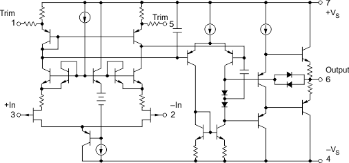
OPA627 Simplified Schematic
