SCPS068J July 2001 – March 2015 PCF8574
PRODUCTION DATA.
- 1 Features
- 2 Applications
- 3 Description
- 4 Revision History
- 5 Pin Configuration and Functions
- 6 Specifications
- 7 Parameter Measurement Information
- 8 Detailed Description
- 9 Application and Implementation
- 10Power Supply Recommendations
- 11Layout
- 12Device and Documentation Support
- 13Mechanical, Packaging, and Orderable Information
8 Detailed Description
8.1 Overview
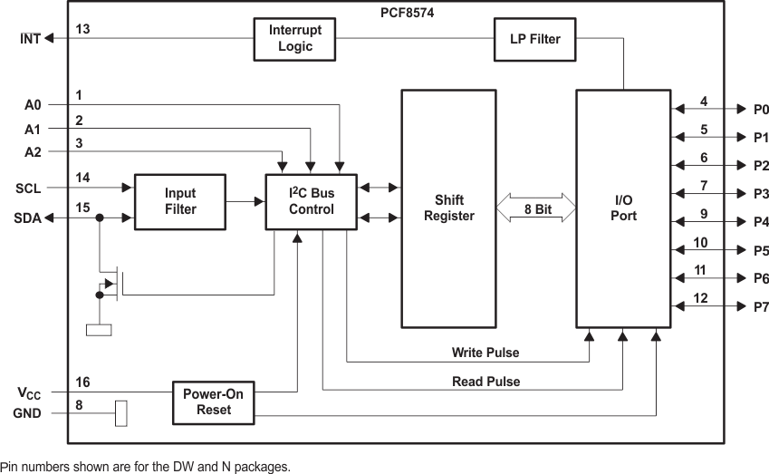
The PCF8574 device is an 8-bit I/O expander for the two-line bidirectional bus (I2C) is designed for 2.5-V to 5.5-V VCC operation. It provides general-purpose remote I/O expansion for most micro-controller families via the I2C interface (serial clock, SCL, and serial data, SDA, pins).
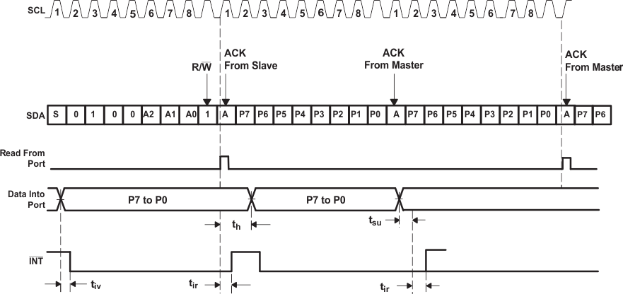
The PCF8574 device provides an open-drain output (INT) that can be connected to the interrupt input of a microcontroller. An interrupt is generated by any rising or falling edge of the port inputs in the input mode. After time, tiv, INT is valid. Resetting and reactivating the interrupt circuit is achieved when data on the port is changed to the original setting or data is read from, or written to, the port that generated the interrupt. Resetting occurs in the read mode at the acknowledge bit after the rising edge of the SCL signal, or in the write mode at the acknowledge bit after the high-to-low transition of the SCL signal. Interrupts that occur during the acknowledge clock pulse can be lost (or be very short) due to the resetting of the interrupt during this pulse. Each change of the I/Os after resetting is detected and, after the next rising clock edge, is transmitted as INT. Reading from, or writing to, another device does not affect the interrupt circuit. This device does not have internal configuration or status registers. Instead, read or write to the device I/Os directly after sending the device address (see Figure 16 and Figure 17).
By sending an interrupt signal on this line, the remote I/O can inform the microcontroller if there is incoming data on its ports without having to communicate by way of the I2C bus. Therefore, PCF8574 can remain a simple slave device.
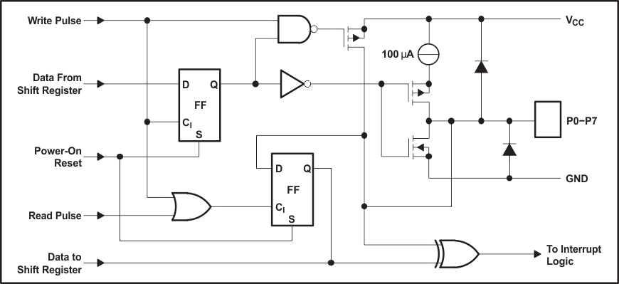
An additional strong pullup to VCC allows fast rising edges into heavily loaded outputs. This device turns on when an output is written high and is switched off by the negative edge of SCL. The I/Os should be high before being used as inputs.
8.2 Functional Block Diagram
8.2.1 Simplified Block Diagram of Device

8.2.2 Simplified Schematic Diagram of Each P-Port Input/Output

8.3 Feature Description
8.3.1 I2C Interface
I2C communication with this device is initiated by a master sending a start condition, a high-to-low transition on the SDA I/O while the SCL input is high. After the start condition, the device address byte is sent, most-significant bit (MSB) first, including the data direction bit (R/W). This device does not respond to the general call address. After receiving the valid address byte, this device responds with an acknowledge, a low on the SDA I/O during the high of the acknowledge-related clock pulse. The address inputs (A0–A2) of the slave device must not be changed between the start and the stop conditions.
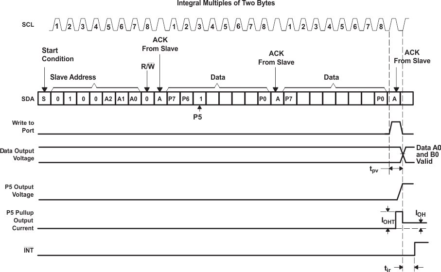
The data byte follows the address acknowledge. If the R/W bit is high, the data from this device are the values read from the P port. If the R/W bit is low, the data are from the master, to be output to the P port. The data byte is followed by an acknowledge sent from this device. If other data bytes are sent from the master, following the acknowledge, they are ignored by this device. Data are output only if complete bytes are received and acknowledged. The output data will be valid at time, tpv, after the low-to-high transition of SCL and during the clock cycle for the acknowledge.
A stop condition, which is a low-to-high transition on the SDA I/O while the SCL input is high, is sent by the master.
8.3.2 Interface Definition
| BYTE | BIT | |||||||
|---|---|---|---|---|---|---|---|---|
| 7 (MSB) | 6 | 5 | 4 | 3 | 2 | 1 | 0 (LSB) | |
| I2C slave address | L | H | L | L | A2 | A1 | A0 | R/W |
| I/O data bus | P7 | P6 | P5 | P4 | P3 | P2 | P1 | P0 |
8.3.3 Address Reference
| INPUTS | I2C BUS SLAVE 8-BIT READ ADDRESS | I2C BUS SLAVE 8-BIT WRITE ADDRESS | ||
|---|---|---|---|---|
| A2 | A1 | A0 | ||
| L | L | L | 65 (decimal), 41 (hexadecimal) | 64 (decimal), 40 (hexadecimal) |
| L | L | H | 67 (decimal), 43 (hexadecimal) | 66 (decimal), 42 (hexadecimal) |
| L | H | L | 69 (decimal), 45 (hexadecimal) | 68 (decimal), 44 (hexadecimal) |
| L | H | H | 71 (decimal), 47 (hexadecimal) | 70 (decimal), 46 (hexadecimal) |
| H | L | L | 73 (decimal), 49 (hexadecimal) | 72 (decimal), 48 (hexadecimal) |
| H | L | H | 75 (decimal), 4B (hexadecimal) | 74 (decimal), 4A (hexadecimal) |
| H | H | L | 77 (decimal), 4D (hexadecimal) | 76 (decimal), 4C (hexadecimal) |
| H | H | H | 79 (decimal), 4F (hexadecimal) | 78 (decimal), 4E (hexadecimal) |
8.4 Device Functional Modes
Figure 16 and Figure 17 show the address and timing diagrams for the write and read modes, respectively.
 Figure 16. Write Mode (Output)
