SLES248A May 2009 – March 2015 PCM1795
PRODUCTION DATA.
- 1 Features
- 2 Applications
- 3 Description
- 4 Revision History
- 5 Pin Configuration and Functions
- 6 Specifications
-
7 Detailed Description
- 7.1 Overview
- 7.2 Functional Block Diagram
- 7.3 Feature Description
- 7.4 Device Functional Modes
- 7.5 Programming
- 7.6
Register Maps
- 7.6.1
Mode Control Registers
- 7.6.1.1 User-Programmable Mode Controls
- 7.6.1.2 Register Map
- 7.6.1.3
Register Definitions
- 7.6.1.3.1 R/W: Read/Write Mode Select
- 7.6.1.3.2 ATx[7:0]: Digital Attenuation Level Setting
- 7.6.1.3.3 R/W: Read/Write Mode Select
- 7.6.1.3.4 ATLD: Attenuation Load Control
- 7.6.1.3.5 FMT[2:0]: Audio Interface Data Format
- 7.6.1.3.6 DMF[1:0]: Sampling Frequency Selection for the De-Emphasis Function
- 7.6.1.3.7 DME: Digital De-Emphasis Control
- 7.6.1.3.8 MUTE: Soft Mute Control
- 7.6.1.3.9 R/W: Read/Write Mode Select
- 7.6.1.3.10 REV: Output Phase Reversal
- 7.6.1.3.11 ATS[1:0]: Attenuation Rate Select
- 7.6.1.3.12 OPE: DAC Operation Control
- 7.6.1.3.13 DFMS: Stereo DF Bypass Mode Select
- 7.6.1.3.14 FLT: Digital Filter Roll-Off Control
- 7.6.1.3.15 INZD: Infinite Zero Detect Mute Control
- 7.6.1.3.16 R/W: Read/Write Mode Select
- 7.6.1.3.17 SRST: System Reset Control
- 7.6.1.3.18 DSD: DSD Interface Mode Control
- 7.6.1.3.19 DFTH: Digital Filter Bypass (or Through Mode) Control
- 7.6.1.3.20 MONO: Monaural Mode Selection
- 7.6.1.3.21 CHSL: Channel Selection for Monaural Mode
- 7.6.1.3.22 OS[1:0]: ΔΣ Oversampling Rate Selection
- 7.6.1.3.23 R/W: Read/Write Mode Select
- 7.6.1.3.24 DZ[1:0]: DSD Zero Output Enable
- 7.6.1.3.25 PCMZ: PCM Zero Output Enable
- 7.6.1.3.26 R: Read Mode Select
- 7.6.1.3.27 ZFGx: Zero-Detection Flag
- 7.6.1.3.28 Read Mode Select
- 7.6.1.3.29 ID[4:0]: Device ID
- 7.6.1
Mode Control Registers
-
8 Application and Implementation
- 8.1 Application Information
- 8.2
Typical Applications
- 8.2.1 Typical Connection Diagram in PCM Mode
- 8.2.2
Application for External Digital Filter Interface
- 8.2.2.1 Design Requirements
- 8.2.2.2 Detailed Design Procedure
- 8.2.2.3 Application Curves
- 8.2.3 Application for DSD Format (DSD Mode) Interface
- 8.2.4
TDMCA Interface Format
- 8.2.4.1 Design Requirements
- 8.2.4.2
Detailed Design Procedure
- 8.2.4.2.1 TDMCA Mode Determination
- 8.2.4.2.2 TDMCA Terminals
- 8.2.4.2.3 Device ID Determination
- 8.2.4.2.4 TDMCA Frame
- 8.2.4.2.5
Command Field
- 8.2.4.2.5.1 Bit 31: Device ID Enable Flag
- 8.2.4.2.5.2 Bit 30: Extended Command Enable Flag
- 8.2.4.2.5.3 Bit 29: Daisy-Chain Selection Flag
- 8.2.4.2.5.4 Bits[28:24]: Device ID
- 8.2.4.2.5.5 Bit 23: Command Read/Write flag
- 8.2.4.2.5.6 Bits[22:16]: Register ID
- 8.2.4.2.5.7 Bits[15:8]: Command data
- 8.2.4.2.5.8 Bits[7:0]: Not used
- 8.2.4.2.6 Extended Command Field
- 8.2.4.2.7 Audio Fields
- 8.2.4.2.8 TDMCA Register Requirements
- 8.2.4.2.9 Register Write/Read Operation
- 8.2.4.2.10 TDMCA Mode Operation
- 9 Power Supply Recommendations
- 10Layout
- 11Device and Documentation Support
- 12Mechanical, Packaging, and Orderable Information
7 Detailed Description
7.1 Overview
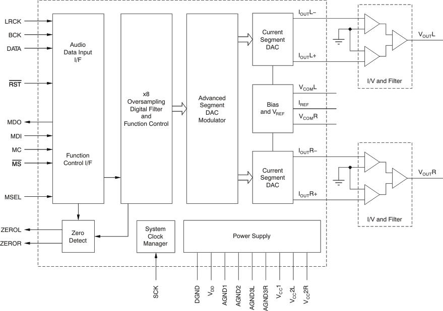
The PCM1795 is a 32-bit, 192 kHz, differential current output stereo DAC that comes in a 28-pin SSOP package. The PCM1795 device is software controlled through I2C or SPI, and utilizes the advanced segment DAC architecture from TI in order to perform with a Stereo Dynamic Range of 123 dB (126 dB Mono) and SNR of 123 dB (126 dB Mono) with a THD of 0.0005%. The balanced current outputs allow the user to customize the analog performance externally.
The PCM1795 device will use the SCK input as its system clock and automatically detect the sampling rate of the digital audio input and has a high tolerance for clock jitter. The PCM1795 device supports both PCM and DSD formats for audio input along with the TDMA or time-division-multiplexed command and audio-data format. The internal filter can be bypassed to allow for an external digital filter to be used.
7.2 Functional Block Diagram
7.3 Feature Description
7.3.1 Audio Data Interface
7.3.1.1 Audio Serial Interface
The audio interface port is a three-wire serial port. It includes LRCK (pin 4), BCK (pin 6), and DATA (pin 5). BCK is the serial audio bit clock, and it is used to clock the serial data present on DATA into the serial shift register of the audio interface. Serial data are clocked into the PCM1795 on the rising edge of BCK. LRCK is the serial audio left/right word clock.
The PCM1795 device requires the synchronization of LRCK and the system clock, but does not need a specific phase relation between LRCK and the system clock.
If the relationship between LRCK and the system clock changes more than ±6 BCK, internal operation is initialized within 1/fS and analog outputs are forced to the bipolar zero level until resynchronization between LRCK and the system clock is completed.
7.3.1.2 PCM Audio Data Formats and Timing
The PCM1795 device supports industry-standard audio data formats, including standard right-justified, I2S, and left-justified. The data formats are illustrated in Figure 35 to Figure 37. Data formats are selected using the format bits, FMT[2:0], in control register 18. The default data format is 32-bit I2S. All formats require binary twos complement, MSB-first audio data. Figure 34 and Table 1 show a detailed timing diagram for the serial audio interface.
 Figure 34. Audio Interface Timing
Table 1. Serial Audio Interface Timing Characteristics for Figure 34
| MIN | MAX | UNIT | ||
|---|---|---|---|---|
| t(BCY) | BCK pulse cycle time | 70 | ns | |
| t(BCL) | BCK pulse duration, low | 30 | ns | |
| t(BCH) | BCK pulse duration, high | 30 | ns | |
| t(BL) | BCK rising edge to LRCK edge | 10 | ns | |
| t(LB) | LRCK edge to BCK rising edge | 10 | ns | |
| t(DS) | DATA setup time | 10 | ns | |
| t(DH) | DATA hold time | 10 | ns | |
| LRCK clock data | 50% ± 2 bit clocks | |||
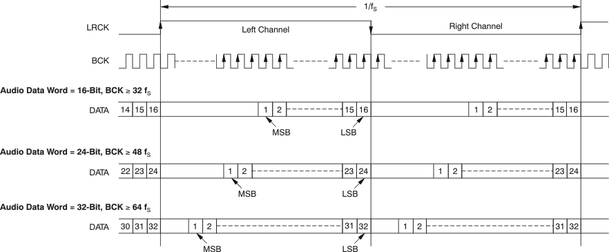 Figure 35. Audio Data Input Format: Standard Data Format (Right-Justified), Left Channel = High, Right Channel = Low
 Figure 36. Audio Data Input Format: Left-Justified Data Format, Left Channel = High, Right Channel = Low
 Figure 37. Audio Data Input Format: I2S Data Format, Left Channel = Low, Right Channel = High
7.3.1.3 External Digital Filter Interface and Timing
The PCM1795 device supports an external digital filter interface that consists of a three- or four-wire synchronous serial port that allows the use of an external digital filter. External filters include the Texas Instruments’ DF1704 and DF1706, the Pacific Microsonics PMD200, or a programmable digital signal processor.
In the external DF mode, LRCK (pin 4), BCK (pin 6) and DATA (pin 5) are defined as: WDCK, the word clock; BCK, the bit clock; and DATA, the monaural data. The external digital filter interface is selected by using the DFTH bit of control register 20, which functions to bypass the internal digital filter of the PCM1795 device .
When the DFMS bit of control register 19 is set, the PCM1795 device can process stereo data. In this case, ZEROL (pin 1) and ZEROR (pin 2) are defined as left-channel data and right-channel data input, respectively.
Detailed information for the external digital filter interface mode is provided in Application For External Digital Filter Interface.
7.3.1.4 Direct Stream Digital (DSD) Format Interface and Timing
The PCM1795 device supports the DSD format interface operation, which includes out-of-band noise filtering using an internal analog FIR filter. For DSD operation, SCK (pin 7) is redefined as BCK, DATA (pin 5) as DATAL (left channel audio data), and LRCK (pin 4) as DATAR (right channel audio data). BCK (pin 6) must be forced low in the DSD mode. The DSD format interface is activated by setting the DSD bit of control register 20.
Detailed information for the DSD mode is provided in Application For DSD Format (DSD Mode) Interface.
7.3.1.5 TDMCA Interface
The PCM1795 device supports the time-division-multiplexed command and audio (TDMCA) data format to enable control of and communication with a number of external devices over a single serial interface.
Detailed information for the TDMCA format is provided in TDMCA Interface Format.
7.3.1.6 Analog Output
Table 2 and Figure 38 show the relationship between the digital input code and analog output.
Table 2. Analog Output Current and Voltage(1)
| PARAMETER | 800000 (–FS) | 000000 (BPZ) | 7FFFFF (+FS) |
|---|---|---|---|
| IOUTN (mA) | –1.5 | –3.5 | –5.5 |
| IOUTP (mA) | –5.5 | 3.5 | –1.5 |
| VOUTN (V) | –1.23 | –2.87 | –4.51 |
| VOUTP (V) | –4.51 | –2.87 | –1.23 |
| VOUT (V) | –2.91 | 0 | 2.91 |
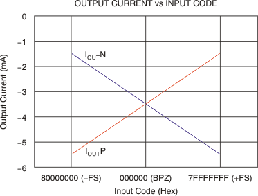 Figure 38. Relationship Between Digital Input and Analog Output
7.4 Device Functional Modes
- SPI Mode is selected by connecting MSEL to DGND. SPI mode uses four signal lines and allows higher speed full-duplex communication between the host and the PCM1795 device.
- I2C Mode is selected by connecting MSEL to VDD. I2C uses two signal lines for half-duplex communication, and used in a variety of devices.
- I2S input Mode is selected by default and is controlled by Register 20 bit 5.
- DSD input Mode is selected by setting Register 20 bit 5 high.
- TDMCA Mode is enabled when the PCM1795 device receives an LRCK signal with a pulse duration of two BCK clocks.
7.5 Programming
7.5.1 System Clock and Reset Functions
7.5.1.1 System Clock Input
The PCM1795 requires a system clock to operate the digital interpolation filters and advanced segment DAC modulators. The system clock is applied at the SCK input (pin 7). The PCM1795 has a system clock detection circuit that automatically senses the frequency at which the system clock is operating. Table 3 shows examples of system clock frequencies for common audio sampling rates. If the oversampling rate of the delta-sigma (ΔΣ) modulator is selected as 128 fS, the system clock frequency is required to be greater than 256 fS.
Figure 39 and Table 4 show the timing requirements for the system clock input. For optimal performance, it is important to use a clock source with low phase jitter and noise. The Texas Instruments PLL1700 family of multiclock generators is an excellent choice to provide the PCM1795 system clock.
Table 3. System Clock Rates for Common Audio Sampling Frequencies
| SAMPLING FREQUENCY (kHz) | SYSTEM CLOCK FREQUENCY (fSCK) (MHz) | |||||
|---|---|---|---|---|---|---|
| 128 fS | 192 fS | 256 fS | 384 fS | 512 fS | 768 fS | |
| 32 | 4.096(1) | 6.144(1) | 8.192 | 12.288 | 16.384 | 24.576 |
| 44.1 | 5.6488(1) | 8.4672 | 11.2896 | 16.9344 | 22.5792 | 33.8688 |
| 48 | 6.144(1) | 9.216 | 12.288 | 18.432 | 24.576 | 36.864 |
| 96 | 12.288 | 18.432 | 24.576 | 36.864 | 49.152(1) | 73.728(1) |
| 192 | 24.576 | 36.864 | 49.152(1) | 73.728(1) | X(2) | X(2) |
 Figure 39. System Clock Input Timing
Table 4. System Clock Input Timing Characteristics for Figure 39
| MIN | MAX | UNIT | ||
|---|---|---|---|---|
| t(SCY) | System clock pulse cycle time | 13 | ns | |
| t(SCKH) | System clock pulse duration, high | 0.4t(SCY) | ns | |
| t(SCKL) | System clock pulse duration, low | 0.4t(SCY) | ns | |
7.5.1.2 Power-On and External Reset Functions
The PCM1795 includes a power-on reset function, as shown in Figure 40. With VDD > 2 V, the power-on reset function is enabled. The initialization sequence requires 1024 system clocks from the time VDD > 2 V. After the initialization period, the PCM1795 is set to its default reset state, as described in Mode Control Registers.
The PCM1795 also includes an external reset capability using the RST input (pin 14). This feature allows an external controller or master reset circuit to force the PCM1795 to initialize to the default reset state.
Figure 41 and Table 5 show the external reset operation and timing. The RST pin is set to logic 0 for a minimum of 20 ns. The RST pin is then set to a logic 1 state, thus starting the initialization sequence that requires 1024 system clock periods. The external reset is especially useful in applications where there is a delay between the PCM1795 power-up and system clock activation.
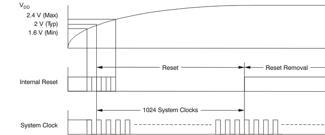 Figure 40. Power-On Reset Timing
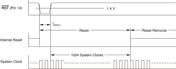 Figure 41. External Reset Timing
Table 5. External Reset Timing Characteristics for Figure 41
| MIN | MAX | UNIT | ||
|---|---|---|---|---|
| t(RST) | Reset pulse duration, low | 20 | ns | |
7.5.2 Function Descriptions
7.5.2.1 Zero Detect
The PCM1795 has a zero-detect function. When the PCM1795 detects the zero conditions as shown in Table 6, the PCM1795 sets ZEROL (pin 1) and ZEROR (pin 2) high.
Table 6. Zero Conditions
| MODE | DETECTING CONDITION AND TIME | |
|---|---|---|
| PCM | DATA is continuously low for 1024 LRCKs. | |
| External DF mode | DATA is continuously low for 1024 WDCKs. | |
| DSD | DZ0 | There are an equal number of 1s and 0s in every 8 bits of DSD input data for 23 ms. |
| DZ1 | The input data are continuously 1001 0110 for 23 ms. | |
7.5.3 Serial Control Interface
The PCM1795 supports both SPI and I2C interfaces that set the mode control registers; see Table 10. The serial control interface is selected by MSEL (pin 3); SPI is activated when MSEL is set low, and I2C is activated when MSEL is set high.
7.5.3.1 SPI Interface
The SPI interface is a four-wire synchronous serial port that operates asynchronously to the serial audio interface and the system clock (SCK). The serial control interface is used to program and read the on-chip mode registers. The control interface includes MDO (pin 13), MDI (pin 11), MC (pin 12), and MS (pin 10). MDO is the serial data output, used to read back the values of the mode registers; MDI is the serial data input, used to program the mode registers; MC is the serial bit clock, used to shift data in and out of the control port; and MS is the mode control enable, used to enable the internal mode register access.
7.5.3.2 Register Read/Write Operation
All read/write operations for the serial control port use 16-bit data words. Figure 42 shows the control data word format. The most significant bit (MSB) is the read/write (R/W) bit. For write operations, the R/W bit must be set to '0'. For read operations, the R/W bit must be set to '1'. There are 7 bits, labeled IDX[6:0], that hold the register index (or address) for the read and write operations. The least significant 8 bits, D[7:0], contain the data to be written to, or the data that was read from, and the register specified by IDX[6:0].
Figure 43 shows the functional timing diagram for writing or reading the serial control port. MS is held at a logic 1 state until a register must be written to or read from. To start the register write or read cycle, MS is set to logic 0. Sixteen clocks are then provided on MC, corresponding to the 16 bits of the control data word on MDI and readback data on MDO. After the eighth clock cycle has completed, the data from the indexed-mode control register appears on MDO during the read operation. After the 16th clock cycle has completed, the data are latched into the indexed-mode control register during the write operation. To write or read subsequent data, MS must be set to '1' once.
 Figure 42. Control Data Word Format for MDI

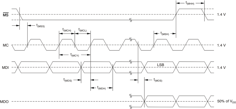 Figure 44. Control Interface Timing
Table 7. Control Interface Timing Characteristics for Figure 44
| MIN | MAX | UNIT | ||
|---|---|---|---|---|
| t(MCY) | MC pulse cycle time | 100 | ns | |
| t(MCL) | MC low-level time | 40 | ns | |
| t(MCH) | MC high-level time | 40 | ns | |
| t(MHH) | MS high-level time | 80 | ns | |
| t(MSS) | MS falling edge to MC rising edge | 15 | ns | |
| t(MSH) | MS hold time(1) | 15 | ns | |
| t(MDH) | MDI hold time | 15 | ns | |
| t(MDS) | MDI setup time | 15 | ns | |
| t(MOS) | MC falling edge to MDO stable | 30 | ns | |
7.5.4 I2C Interface
The PCM1795 supports the I2C serial bus and the data transmission protocol for standard and fast mode as a slave device. This protocol is explained in the I2C specification 2.0.
In I2C mode, the control terminals are changed as described in Table 8.
Table 8. Control Terminals
| TERMINAL NAME | TDMCA NAME | PROPERTY | DESCRIPTION |
|---|---|---|---|
| MS | ADR0 | Input | I2C address 0 |
| MDI | ADR1 | Input | I2C address 1 |
| MC | SCL | Input | I2C clock |
| MDO | SDA | Input/output | I2C data |
7.5.4.1 Slave Address
The PCM1795 has 7 bits for its own slave address, as shown in Figure 45. The first 5 bits (MSBs) of the slave address are factory preset to 10011. The next 2 bits of the address byte are the device select bits that can be user-defined by the ADR1 and ADR0 terminals. A maximum of four PCM1795 devicess can be connected on the same bus at one time. Each PCM1795 responds when it receives its own slave address.
 Figure 45. Slave Address
7.5.4.2 Packet Protocol
A master device must control packet protocol that consists of a start condition, slave address, read/write bit, data if write or acknowledge if read, and stop condition. The PCM1795 supports only slave receivers and slave transmitters.
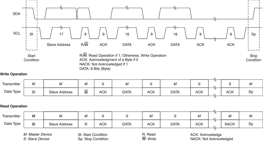 Figure 46. Basic I2C Framework
7.5.4.3 Write Register
A master can write to any PCM1795 registers using single or multiple accesses. The master sends a PCM1795 slave address with a write bit, a register address, and the data. If multiple access is required, the address is that of the starting register, followed by the data to be transferred. When the data are received properly, the index register is incremented by '1' automatically. When the index register reaches 0x7F, the next value is 0x00. When undefined registers are accessed, the PCM1795 does not send an acknowledgment. Figure 47 shows a diagram of the write operation.
 Figure 47. Write Operation
7.5.4.4 Read Register
A master can read the PCM1795 register. The value of the register address is stored in an indirect index register in advance. The master sends a PCM1795 slave address with a read bit after storing the register address. Then the PCM1795 transfers the data that the index register points to. When the data are transferred during a multiple access, the index register is incremented by '1' automatically. (When first going into read mode immediately following a write, the index register is not incremented. The master can read the register that was previously written.) When the index register reaches 0x7F, the next value is 0x00. The PCM1795 outputs some data when the index register is 0x10 to 0x1F, even if it is not defined in Table 10. Figure 48 shows a diagram of the read operation.
 Figure 48. Read Operation
7.5.4.5 Noise Suppression
The PCM1795 incorporates noise suppression using the system clock (SCK). However, there must be no more than two noise spikes in 600 ns. The noise suppression works for SCK frequencies between 8 MHz and 40 MHz in fast mode. However, it works incorrectly under the following conditions:
Case 1:
- t(SCK) > 120 ns (t(SCK): period of SCK)
- t(HI) + t(D–HD) < t(SCK) × 5
- Spike noise exists on the first half of the SCL high pulse.
- Spike noise exists on the SDA high pulse just before SDA goes low.
 Figure 49. Case 1
When these conditions occur at the same time, the data are recognized as low.
Case 2:
- t(SCK) > 120 ns
- t(S–HD) or t(RS–HD) < t(SCK) × 5
- Spike noise exists on both SCL and SDA during the hold time.
 Figure 50. Case 2
When these conditions occur at the same time, the PCM1795 fails to detect a start condition.
Case 3:
- t(SCK) < 50 ns
- t(SP) > t(SCK)
- Spike noise exists on SCL just after SCL goes low.
- Spike noise exists on SDA just before SCL goes low.
 Figure 51. Case 3
When these conditions occur at the same time, the PCM1795 erroneously detects a start or stop condition.
7.6 Register Maps
7.6.1 Mode Control Registers
7.6.1.1 User-Programmable Mode Controls
The PCM1795 device includes a number of user-programmable functions that are accessed via mode control registers. The registers are programmed using the serial control interface, as previously discussed in SPI Interface and I2C Interface. Table 9 lists the available mode-control functions, along with the default reset conditions and associated register index.
Table 9. User-Programmable Function Controls
| FUNCTION | DEFAULT | REGISTER | BIT | PCM | DSD | DF BYPASS | |
|---|---|---|---|---|---|---|---|
| Digital attenuation control | 0 dB | Register 16 | ATL[7:0] (for left channel) | Yes | No | No | |
| 0 dB to –120 dB and mute, 0.5-dB step | Register 17 | ATR[7:0] (for right channel) | |||||
| Attenuation load control | Attenuation disabled | Register 18 | ATLD | Yes | No | No | |
| Disabled, enabled | |||||||
| Input audio data format selection | 24-bit I2S format | Register 18 | FMT[2:0] | Yes | No | Yes | |
| 16-, 20-, 32-bit standard (right-justified) format 24-bit MSB-first left-justified format 16-/32-bit I2S format |
|||||||
| Sampling rate selection for de-emphasis | De-emphasis disabled | Register 18 | DMF[1:0] | Yes | Yes(1) | No | |
| Disabled, 44.1 kHz, 48 kHz, 32 kHz | |||||||
| De-emphasis control | De-emphasis disabled | Register 18 | DME | Yes | No | No | |
| Disabled, enabled | |||||||
| Soft mute control | Mute disabled | Register 18 | MUTE | Yes | No | No | |
| Soft mute disabled, enabled | |||||||
| Output phase reversal | Normal | Register 19 | REV | Yes | Yes | Yes | |
| Normal, reverse | |||||||
| Attenuation speed selection | ×1 fS | Register 19 | ATS[1:0] | Yes | No | No | |
| ×1fS, ×(1/2)fS, ×(1/4)fS, ×(1/8)fS | |||||||
| DAC operation control | DAC operation enabled | Register 19 | OPE | Yes | Yes | Yes | |
| Enabled, disabled | |||||||
| Stereo DF bypass mode select | Monaural | Register 19 | DFMS | Yes | No | Yes | |
| Monaural, stereo | |||||||
| Digital filter roll-off selection | Sharp roll-off | Register 19 | FLT | Yes | No | No | |
| Sharp roll-off, slow roll-off | |||||||
| Infinite zero mute control | Disabled | Register 19 | INZD | Yes | No | Yes | |
| Disabled, enabled | |||||||
| System reset control | Normal operation | Register 20 | SRST | Yes | Yes | Yes | |
| Reset operation, normal operation | |||||||
| DSD interface mode control | Disabled | Register 20 | DSD | Yes | Yes | No | |
| DSD enabled, disabled | |||||||
| Digital-filter bypass control | DF enabled | Register 20 | DFTH | Yes | No | Yes | |
| DF enabled, DF bypass | |||||||
| Monaural mode selection | Stereo | Register 20 | MONO | Yes | Yes | Yes | |
| Stereo, monaural | |||||||
| Channel selection for monaural mode data | Left channel | Register 20 | CHSL | Yes | Yes | Yes | |
| Left channel, Right channel | |||||||
| ΔΣ oversampling rate selection | ×64 fS | Register 20 | OS[1:0] | Yes | Yes(2) | Yes | |
| ×64 fS, ×128 fS, ×32 fS | |||||||
| PCM zero output enable | Enabled | Register 21 | PCMZ | Yes | No | Yes | |
| DSD zero output enable | Disabled | Register 21 | DZ[1:0] | Yes | Yes | No | |
| FUNCTION AVAILABLE ONLY FOR READ | |||||||
| Zero detection flag | Not zero = 0 | Register 22 | ZFGL (for left channel) | Yes | Yes | Yes | |
| Not zero, zero detected | Zero detected = 1 | ZFGR (for right channel) | |||||
| Device ID (at TDMCA) | — | Register 23 | ID[4:0] | Yes | No | No | |
7.6.1.2 Register Map
The mode control register map is shown in Table 10. Registers 16 to 21 include an R/W bit that determines whether a register read (R/W = 1) or write (R/W = 0) operation is performed. Registers 22 and 23 are read-only.
Table 10. Mode Control Register Map
| REGISTER | B15 | B14 | B13 | B12 | B11 | B10 | B9 | B8 | B7 | B6 | B5 | B4 | B3 | B2 | B1 | B0 |
|---|---|---|---|---|---|---|---|---|---|---|---|---|---|---|---|---|
| Register 16 | R/W | 0 | 0 | 1 | 0 | 0 | 0 | 0 | ATL7 | ATL6 | ATL5 | ATL4 | ATL3 | ATL2 | ATL1 | ATL0 |
| Register 17 | R/W | 0 | 0 | 1 | 0 | 0 | 0 | 1 | ATR7 | ATR6 | ATR5 | ATR4 | ATR3 | ATR2 | ATR1 | ATR0 |
| Register 18 | R/W | 0 | 0 | 1 | 0 | 0 | 1 | 0 | ATLD | FMT2 | FMT1 | FMT0 | DMF1 | DMF0 | DME | MUTE |
| Register 19 | R/W | 0 | 0 | 1 | 0 | 0 | 1 | 1 | REV | ATS1 | ATS0 | OPE | RSV | DFMS | FLT | INZD |
| Register 20 | R/W | 0 | 0 | 1 | 0 | 1 | 0 | 0 | RSV | SRST | DSD | DFTH | MONO | CHSL | OS1 | OS0 |
| Register 21 | R/W | 0 | 0 | 1 | 0 | 1 | 0 | 1 | RSV | RSV | RSV | RSV | RSV | DZ1 | DZ0 | PCMZ |
| Register 22 | R | 0 | 0 | 1 | 0 | 1 | 1 | 0 | RSV | RSV | RSV | RSV | RSV | RSV | ZFGR | ZFGL |
| Register 23 | R | 0 | 0 | 1 | 0 | 1 | 1 | 1 | RSV | RSV | RSV | ID4 | ID3 | ID2 | ID1 | ID0 |
7.6.1.3 Register Definitions

7.6.1.3.1 R/W: Read/Write Mode Select
When R/W = 0, a write operation is performed.
When R/W = 1, a read operation is performed.
Default value: 0
7.6.1.3.2 ATx[7:0]: Digital Attenuation Level Setting
These bits are available for read and write.
Default value: 1111 1111b
Each DAC output has a digital attenuator associated with it. The attenuator can be set from 0 dB to –120 dB, in 0.5-dB steps. Alternatively, the attenuator can be set to infinite attenuation (or mute). The attenuation data for each channel can be set individually. However, the data load control (the ATLD bit of control register 18) is common to both attenuators. ATLD must be set to '1' in order to change an attenuator setting. The attenuation level can be set using Equation 1.
where
For ATx[7:0]DEC = 0 through 14, the attenuator is set to infinite attenuation. Table 11 lists the attenuation levels for various settings.
Table 11. Attenuation Levels
| ATx[7:0] | DECIMAL VALUE | ATTENUATION LEVEL SETTING |
|---|---|---|
| 1111 1111b | 255 | 0 dB, no attenuation (default) |
| 1111 1110b | 254 | –0.5 dB |
| 1111 1101b | 253 | –1.0 dB |
| — | — | — |
| 0001 0000b | 16 | –119.5 dB |
| 0000 1111b | 15 | –120.0 dB |
| 0000 1110b | 14 | Mute |
| — | — | — |
| 0000 0000b | 0 | Mute |

7.6.1.3.3 R/W: Read/Write Mode Select
When R/W = 0, a write operation is performed.
When R/W = 1, a read operation is performed.
Default value: 0
7.6.1.3.4 ATLD: Attenuation Load Control
This bit is available for read and write.
Default value: 0
Table 12. ATLD
| ATLD | ATTENUATION CONTROL SETTING |
|---|---|
| ATLD = 0 | Attenuation control disabled (default) |
| ATLD = 1 | Attenuation control enabled |
The ATLD bit is used to enable loading of the attenuation data contained in registers 16 and 17. When ATLD = 0, the attenuation settings remain at the previously programmed levels, ignoring new data loaded from registers 16 and 17. When ATLD = 1, attenuation data written to registers 16 and 17 is loaded normally.
7.6.1.3.5 FMT[2:0]: Audio Interface Data Format
These bits are available for read and write.
Default value: 101
Table 13. FMT[2:0]
| FMT[2:0] | AUDIO DATA FORMAT SELECTION |
|---|---|
| 000 | 16-bit standard format, right-justified data, BCK ≥ x32 fS |
| 001 | 32-bit standard format, right-justified data, BCK ≥ x64 fS |
| 010 | 24-bit standard format, right-justified data, BCK ≥ x48 fS |
| 011 | 24-bit MSB-first, left-justified format data, BCK ≥ x48 fS |
| 100 | 32-bit I2S format data, BCK ≥ x64 fS |
| 101 | 24-bit I2S format data (default), BCK ≥ x48 fS |
| 110 | Reserved |
| 111 | Reserved |
The FMT[2:0] bits are used to select the data format for the serial audio interface.
For the external digital filter interface mode (DFTH mode), this register is operated as shown in Application for External Digital Filter Interface.
7.6.1.3.6 DMF[1:0]: Sampling Frequency Selection for the De-Emphasis Function
These bits are available for read and write.
Default value: 00
Table 14. DMF[1:0]
| DMF[1:0] | DE-EMPHASIS SAMPLING FREQUENCY SELECTION |
|---|---|
| 00 | Disabled (default) |
| 01 | 48 kHz |
| 10 | 44.1 kHz |
| 11 | 32 kHz |
The DMF[1:0] bits are used to select the sampling frequency used by the digital de-emphasis function when it is enabled by setting the DME bit. The de-emphasis curves are shown in Typical Characteristics.
For the DSD mode, analog FIR filter performance can be selected using this register. A register map and filter response plots are shown in Application For DSD Format (DSD Mode) Interface.
7.6.1.3.7 DME: Digital De-Emphasis Control
This bit is available for read and write.
Default value: 0
Table 15. DME
| DME | DE-EMPHASIS SETTING |
|---|---|
| DME = 0 | De-emphasis disabled (default) |
| DME = 1 | De-emphasis enabled |
The DME bit is used to enable or disable the de-emphasis function for both channels.
7.6.1.3.8 MUTE: Soft Mute Control
This bit is available for read and write.
Default value: 0
Table 16. MUTE
| MUTE | SOFT MUTE SETTING |
|---|---|
| MUTE = 0 | Soft mute disabled (default) |
| MUTE = 1 | Soft mute enabled |
The MUTE bit is used to enable or disable the soft mute function for both channels.
Soft mute is operated as a 256-step attenuator. The speed for each step to –∞ dB (mute) is determined by the attenuation rate selected in the ATS register.

7.6.1.3.9 R/W: Read/Write Mode Select
When R/W = 0, a write operation is performed.
When R/W = 1, a read operation is performed.
Default value: 0
7.6.1.3.10 REV: Output Phase Reversal
This bit is available for read and write.
Default value: 0
Table 17. REV
| REV | OUTPUT SETTING |
|---|---|
| REV = 0 | Normal output (default) |
| REV = 1 | Inverted output |
The REV bit is used to invert the output phase for both channels.
7.6.1.3.11 ATS[1:0]: Attenuation Rate Select
These bits are available for read and write.
Default value: 00
Table 18. ATS[1:0]
| ATS[1:0] | ATTENUATION RATE SELECTION |
|---|---|
| 00 | Every LRCK (default) |
| 01 | LRCK/2 |
| 10 | LRCK/4 |
| 11 | LRCK/8 |
The ATS[1:0] bits are used to select the rate at which the attenuator is decremented/incremented during level transitions.
7.6.1.3.12 OPE: DAC Operation Control
This bit is available for read and write.
Default value: 0
Table 19. OPE
| OPE | DAC OPERATION CONTROL |
|---|---|
| OPE = 0 | DAC operation enabled (default) |
| OPE = 1 | DAC operation disabled |
The OPE bit is used to enable or disable the analog output for both channels. Disabling the analog outputs forces them to the bipolar zero level (BPZ) even if audio data are present on the input.
7.6.1.3.13 DFMS: Stereo DF Bypass Mode Select
This bit is available for read and write.
Default value: 0
Table 20. DFMS
| DFMS | MODE SELECTION |
|---|---|
| DFMS = 0 | Monaural (default) |
| DFMS = 1 | Stereo input enabled |
The DFMS bit is used to enable stereo operation in DF bypass mode. In the DF bypass mode, when DFMS is set to '0', the pin for the input data are DATA (pin 5) only; therefore, the PCM1795 operates as a monaural DAC. When DFMS is set to '1', the PCM1795 can operate as a stereo DAC with inputs of the left channel and right channel data on ZEROL (pin 1) and ZEROR (pin 2), respectively.
7.6.1.3.14 FLT: Digital Filter Roll-Off Control
This bit is available for read and write.
Default value: 0
Table 21. FLT
| FLT | ROLL-OFF CONTROL |
|---|---|
| FLT = 0 | Sharp roll-off (default) |
| FLT = 1 | Slow roll-off |
The FLT bit is used to select the digital filter roll-off characteristic. The filter responses for these selections are shown in Typical Characteristics.
7.6.1.3.15 INZD: Infinite Zero Detect Mute Control
This bit is available for read and write.
Default value: 0
Table 22. INZD
| INZD | INFINITE ZERO DETECT MUTE SETTING |
|---|---|
| INZD = 0 | Infinite zero detect mute disabled (default) |
| INZD = 1 | Infinite zero detect mute enabled |
The INZD bit is used to enable or disable the zero detect mute function. Setting INZD to '1' forces muted analog outputs to hold a bipolar zero level when the PCM1795 detects a zero condition in both channels. The infinite zero detect mute function is not available in the DSD mode.

7.6.1.3.16 R/W: Read/Write Mode Select
When R/W = 0, a write operation is performed.
When R/W = 1, a read operation is performed.
Default value: 0
7.6.1.3.17 SRST: System Reset Control
This bit is available for write only.
Default value: 0
Table 23. SRST
| SRST | SYSTEM RESET CONTROL |
|---|---|
| SRST = 0 | Normal operation (default) |
| SRST = 1 | System reset operation (generate one reset pulse) |
The SRST bit is used to reset the PCM1795 to the initial system condition.
7.6.1.3.18 DSD: DSD Interface Mode Control
This bit is available for read and write.
Default value: 0
Table 24. DSD
| DSD | DSD INTERFACE MODE CONTROL |
|---|---|
| DSD = 0 | DSD interface mode disabled (default) |
| DSD = 1 | DSD interface mode enabled |
The DSD bit is used to enable or disable the DSD interface mode.
7.6.1.3.19 DFTH: Digital Filter Bypass (or Through Mode) Control
This bit is available for read and write.
Default value: 0
Table 25. DFTH
| DFTH | DIGITAL FILTER CONTROL |
|---|---|
| DFTH = 0 | Digital filter enabled (default) |
| DFTH = 1 | Digital filter bypassed for external digital filter |
The DFTH bit is used to enable or disable the external digital filter interface mode.
7.6.1.3.20 MONO: Monaural Mode Selection
This bit is available for read and write.
Default value: 0
Table 26. MONO
| MONO | MODE SELECTION |
|---|---|
| MONO = 0 | Stereo mode (default) |
| MONO = 1 | Monaural mode |
The MONO function is used to change operation mode from the normal stereo mode to the monaural mode. When the monaural mode is selected, both DACs operate in a balanced mode for one channel of audio input data. Channel selection is available for left-channel or right-channel data, determined by the CHSL bit.
7.6.1.3.21 CHSL: Channel Selection for Monaural Mode
This bit is available for read and write.
Default value: 0
Table 27. CHSL
| CHSL | CHANNEL SELECTION |
|---|---|
| CHSL = 0 | Left channel selected (default) |
| CHSL = 1 | Right channel selected |
This bit is available when MONO = 1.
The CHSL bit selects left-channel or right-channel data to be used in monaural mode.
7.6.1.3.22 OS[1:0]: ΔΣ Oversampling Rate Selection
These bits are available for read and write.
Default value: 00
Table 28. OS[1:0]
| OS[1:0] | OPERATING SPEED SELECTION |
|---|---|
| 00 | 64 times fS (default) |
| 01 | 32 times fS |
| 10 | 128 times fS |
| 11 | Reserved |
The OS bits are used to change the oversampling rate of ΔΣ modulation. Use of this function enables the designer to stabilize the conditions at the post low-pass filter for different sampling rates. As an application example, programming to set 128 times in 44.1-kHz operation, 64 times in 96-kHz operation, or 32 times in 192-kHz operation allows the use of only a single type (cut-off frequency) of post low-pass filter. The 128-fS oversampling rate is not available at sampling rates above 100 kHz. If the 128-fS oversampling rate is selected, a system clock of more than 256 fS is required.
In DSD mode, these bits are used to select the speed of the bit clock for DSD data coming into the analog FIR filter.

7.6.1.3.23 R/W: Read/Write Mode Select
When R/W = 0, a write operation is performed.
When R/W = 1, a read operation is performed.
Default value: 0
7.6.1.3.24 DZ[1:0]: DSD Zero Output Enable
These bits are available for read and write.
Default value: 00
Table 29. DZ[1:0]
| DZ[1:0] | ZERO OUTPUT ENABLE |
|---|---|
| 00 | Disabled (default) |
| 01 | Even pattern detect 1 × 96h pattern detect |
The DZ bits are used to enable or disable the output zero flags and to select the zero pattern in DSD mode.
7.6.1.3.25 PCMZ: PCM Zero Output Enable
These bits are available for read and write.
Default value: 1
Table 30. PCMZ
| PCMZ | PCM ZERO OUTPUT SETTING |
|---|---|
| PCMZ = 0 | PCM zero output disabled |
| PCMZ = 1 | PCM zero output enabled (default) |
The PCMZ bit is used to enable or disable the output zero flags in PCM mode and the external DF mode.

7.6.1.3.26 R: Read Mode Select
Value is always '1', specifying the readback mode.
7.6.1.3.27 ZFGx: Zero-Detection Flag
Where x = L or R, corresponding to the DAC output channel. These bits are available only for readback.
Default value: 00
Table 31. ZFGx
| ZFGx | ZERO DETECTION |
|---|---|
| ZFGx = 0 | Not zero |
| ZFGx = 1 | Zero detected |
These bits show zero conditions. The status is the same as that of the zero flags at ZEROL (pin 1) and ZEROR (pin 2). See Zero Detect.

7.6.1.3.28 Read Mode Select
Value is always '1', specifying the readback mode.
7.6.1.3.29 ID[4:0]: Device ID
The ID[4:0] bits hold a device ID in the TDMCA mode.