SLES248A May 2009 – March 2015 PCM1795
PRODUCTION DATA.
- 1 Features
- 2 Applications
- 3 Description
- 4 Revision History
- 5 Pin Configuration and Functions
- 6 Specifications
-
7 Detailed Description
- 7.1 Overview
- 7.2 Functional Block Diagram
- 7.3 Feature Description
- 7.4 Device Functional Modes
- 7.5 Programming
- 7.6
Register Maps
- 7.6.1
Mode Control Registers
- 7.6.1.1 User-Programmable Mode Controls
- 7.6.1.2 Register Map
- 7.6.1.3
Register Definitions
- 7.6.1.3.1 R/W: Read/Write Mode Select
- 7.6.1.3.2 ATx[7:0]: Digital Attenuation Level Setting
- 7.6.1.3.3 R/W: Read/Write Mode Select
- 7.6.1.3.4 ATLD: Attenuation Load Control
- 7.6.1.3.5 FMT[2:0]: Audio Interface Data Format
- 7.6.1.3.6 DMF[1:0]: Sampling Frequency Selection for the De-Emphasis Function
- 7.6.1.3.7 DME: Digital De-Emphasis Control
- 7.6.1.3.8 MUTE: Soft Mute Control
- 7.6.1.3.9 R/W: Read/Write Mode Select
- 7.6.1.3.10 REV: Output Phase Reversal
- 7.6.1.3.11 ATS[1:0]: Attenuation Rate Select
- 7.6.1.3.12 OPE: DAC Operation Control
- 7.6.1.3.13 DFMS: Stereo DF Bypass Mode Select
- 7.6.1.3.14 FLT: Digital Filter Roll-Off Control
- 7.6.1.3.15 INZD: Infinite Zero Detect Mute Control
- 7.6.1.3.16 R/W: Read/Write Mode Select
- 7.6.1.3.17 SRST: System Reset Control
- 7.6.1.3.18 DSD: DSD Interface Mode Control
- 7.6.1.3.19 DFTH: Digital Filter Bypass (or Through Mode) Control
- 7.6.1.3.20 MONO: Monaural Mode Selection
- 7.6.1.3.21 CHSL: Channel Selection for Monaural Mode
- 7.6.1.3.22 OS[1:0]: ΔΣ Oversampling Rate Selection
- 7.6.1.3.23 R/W: Read/Write Mode Select
- 7.6.1.3.24 DZ[1:0]: DSD Zero Output Enable
- 7.6.1.3.25 PCMZ: PCM Zero Output Enable
- 7.6.1.3.26 R: Read Mode Select
- 7.6.1.3.27 ZFGx: Zero-Detection Flag
- 7.6.1.3.28 Read Mode Select
- 7.6.1.3.29 ID[4:0]: Device ID
- 7.6.1
Mode Control Registers
-
8 Application and Implementation
- 8.1 Application Information
- 8.2
Typical Applications
- 8.2.1 Typical Connection Diagram in PCM Mode
- 8.2.2
Application for External Digital Filter Interface
- 8.2.2.1 Design Requirements
- 8.2.2.2 Detailed Design Procedure
- 8.2.2.3 Application Curves
- 8.2.3 Application for DSD Format (DSD Mode) Interface
- 8.2.4
TDMCA Interface Format
- 8.2.4.1 Design Requirements
- 8.2.4.2
Detailed Design Procedure
- 8.2.4.2.1 TDMCA Mode Determination
- 8.2.4.2.2 TDMCA Terminals
- 8.2.4.2.3 Device ID Determination
- 8.2.4.2.4 TDMCA Frame
- 8.2.4.2.5
Command Field
- 8.2.4.2.5.1 Bit 31: Device ID Enable Flag
- 8.2.4.2.5.2 Bit 30: Extended Command Enable Flag
- 8.2.4.2.5.3 Bit 29: Daisy-Chain Selection Flag
- 8.2.4.2.5.4 Bits[28:24]: Device ID
- 8.2.4.2.5.5 Bit 23: Command Read/Write flag
- 8.2.4.2.5.6 Bits[22:16]: Register ID
- 8.2.4.2.5.7 Bits[15:8]: Command data
- 8.2.4.2.5.8 Bits[7:0]: Not used
- 8.2.4.2.6 Extended Command Field
- 8.2.4.2.7 Audio Fields
- 8.2.4.2.8 TDMCA Register Requirements
- 8.2.4.2.9 Register Write/Read Operation
- 8.2.4.2.10 TDMCA Mode Operation
- 9 Power Supply Recommendations
- 10Layout
- 11Device and Documentation Support
- 12Mechanical, Packaging, and Orderable Information
10 Layout
10.1 Layout Guidelines
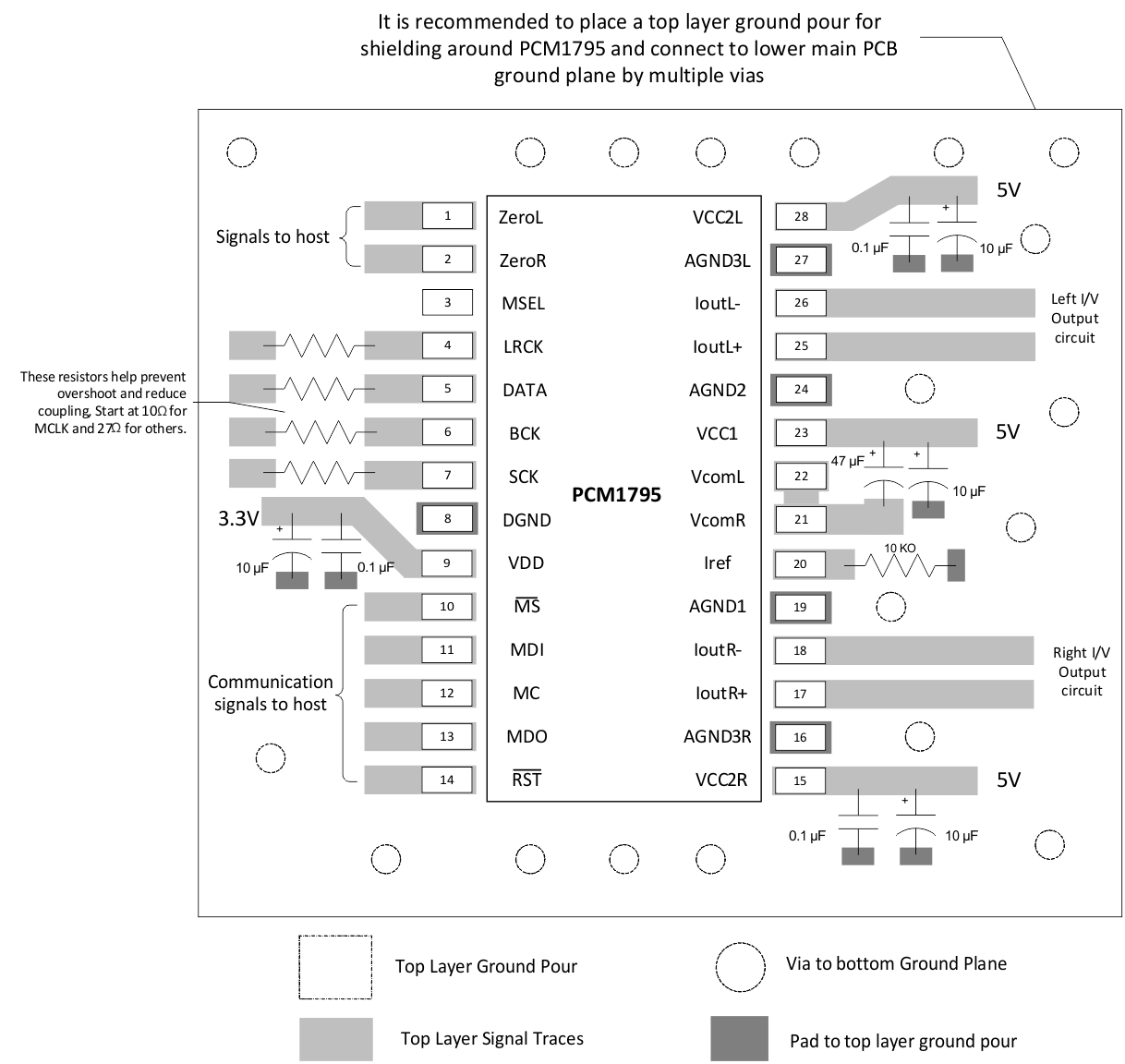
Designers should try to use the same ground between AGND and DGND to avoid any potential voltage difference between them. Ensure that the return currents for digital signals will avoid the AGND pin or the input signals to the I/V stage. Avoid running high-frequency clock and control signals near AGND, or any of the VOUT pins where possible. The pin layout of the PCM1795 device partitions into two sides, the analog side and the digital side. Providing the system is partitioned in such a way that digital signals are routed away from the analog sections, then no digital return currents (for example, clocks) should be generated in the analog circuitry.
- Decoupling capacitors should be placed as close to the VCC1, VCC2L, VCCR2, VCOML, VCOMR, and VDD pins as possible.
- Further guidelines can be found in Figure 83.
10.2 Layout Example
 Figure 83. Layout Recommendation