SLLS977F April 2009 – July 2017 SN75DP139
PRODUCTION DATA.
- 1 Features
- 2 Applications
- 3 Description
- 4 Revision History
- 5 Pin Configuration and Functions
-
6 Specifications
- 6.1 Absolute Maximum Ratings
- 6.2 ESD Ratings
- 6.3 Recommended Operating Conditions
- 6.4 Thermal Information
- 6.5 Electrical Characteristics (Device Power)
- 6.6 Electrical Characteristics (Hot Plug Detect)
- 6.7 Electrical Characteristics (Aux / I2C Pins)
- 6.8 Electrical Characteristics (TMDS and Main Link Pins)
- 6.9 Switching Characteristics (Hot Plug Detect)
- 6.10 Switching Characteristics (Aux / I2C Pins)
- 6.11 Switching Characteristics (TMDS and Main Link Pins)
- 6.12 Typical Characteristics
- 7 Detailed Description
- 8 Application and Implementation
- 9 Power Supply Recommendations
- 10Layout
- 11Device and Documentation Support
- 12Mechanical, Packaging, and Orderable Information
パッケージ・オプション
メカニカル・データ(パッケージ|ピン)
サーマルパッド・メカニカル・データ
発注情報
6 Specifications
6.1 Absolute Maximum Ratings
over operating free-air temperature range (unless otherwise noted)(1)| MIN | MAX | UNIT | ||
|---|---|---|---|---|
| Supply voltage range(2) | VCC | –0.3 | 3.6 | V |
| Voltage range | Main Link Input (IN_Dx) differential voltage | –0.3 | VCC + 0.3 | V |
| TMDS Outputs (OUT_Dx) | –0.3 | VCC + 0.3 | ||
| HPD_SOURCE, SDA_SOURCE, SCL_SOURCE, OVS, DDC_EN, VSadj, SRC, I2C_EN | –0.3 | VCC + 0.3 | ||
| HPD_SINK, SDA_SINK, SCL_SINK, OE_EN, HPDINV | –0.3 | 5.5 | ||
| Storage temperature range, Tstg | –55 | 150 | °C | |
(1) Stresses beyond those listed under Absolute Maximum Ratings may cause permanent damage to the device. These are stress ratings only and functional operation of the device at these or any conditions beyond those indicated under Recommended Operating Conditions is not implied. Exposure to absolute-maximum-rated conditions for extended periods may affect device reliability.
(2) All voltage values, except differential voltages, are with respect to network ground terminal.
6.2 ESD Ratings
| VALUE | UNIT | |||
|---|---|---|---|---|
| V(ESD) | Electrostatic discharge | Human body model(1) | ±10000 | V |
| Charged-device model(2) | ±1500 | |||
| Machine model(3) | ±200 | V | ||
(1) Tested in accordance with JEDEC Standard 22, Test Method A114-B
(2) Tested in accordance with JEDEC Standard 22, Test Method C101-A
(3) Tested in accordance with JEDEC Standard 22, Test Method A115-A
6.3 Recommended Operating Conditions
over operating free-air temperature range (unless otherwise noted)| MIN | NOM | MAX | UNIT | |||
|---|---|---|---|---|---|---|
| VCC | Supply Voltage | 3 | 3.3 | 3.6 | V | |
| TA | Operating free-air temperature | 0 | 85 | °C | ||
| MAIN LINK DIFFERENTIAL INPUT PINS | ||||||
| VID_PP | Peak-to-peak AC input differential voltage | 0.15 | 1.2 | V | ||
| dR | Data rate | RGZ package | 0.25 | 3.4 | Gbps | |
| RSB package | 0.25 | 3.4 | ||||
| trise fall time | Input Signal Rise and Fall time (20%-80%) | 75 | ps | |||
| VPRE | Pre-emphasis on the Input Signal at IN_Dx pins | 0 | 0 | 0 | db | |
| TMDS DIFFERENTIAL OUTPUT PINS | ||||||
| AVCC | TMDS output termination voltage | 3 | 3.3 | 3.6 | V | |
| dR | Data rate | RGZ package | 0.25 | 3.4 | Gbps | |
| RSB package | 0.25 | 3.4 | ||||
| RT | Termination resistance | 45 | 50 | 55 | Ω | |
| RVsadj | TMDS output swing voltage bias resistor(1) | 3.65 | 4.02 | kΩ | ||
| AUXILIARY AND I2C PINS | ||||||
| VI | Input voltage | SDA_SINK, SCL_SINK | 0 | 5.5 | V | |
| SDA_SOURCE, SCL_SOURCE | 3.6 | |||||
| dR(I2C) | I2C data rate | 100 | kHz | |||
| HPD_SINK, HPDINV, OE_N | ||||||
| VIH | High-level input voltage | 2 | 5.5 | V | ||
| VIL | Low-level input voltage | 0 | 0.8 | V | ||
| DDC_EN, I2C_EN | ||||||
| VIH | High-level input voltage | 2 | 3.6 | V | ||
| VIL | Low-level input voltage | 0 | 0.8 | V | ||
| SRC, OVS | ||||||
| VIH_SRC_OVS | High-level input voltage | 3 | 3.6 | V | ||
| VIL_SRC_OVS | Low-level input voltage | 0 | 0.5 | V | ||
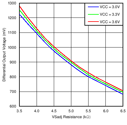
(1) RVsadj resistor controls the SN75DP139 Driver output voltage swing and thus helps in meeting system compliance. It is recommended that RVsadj resistor should be above the MIN value as indicated in the RECOMMENDED OPERATING CONDITIONS table, however for NOM and MAX value, Figure 19 could be used as reference. It is important to note that system level losses, AVCC and RT variation affect RVsadj resistor selection. Worse case variation on system level losses, AVCC, RT could make RVsadj resistor value of 4.02 kΩ ±5% result in non-compliant TMDS output voltage swing. In such cases Figure 19 could be used as reference.
6.4 Thermal Information
over operating free-air temperature range (unless otherwise noted)| PARAMETER | TEST CONDITIONS | MIN | TYP | MAX(1) | UNIT | ||
|---|---|---|---|---|---|---|---|
| θJB | Junction-to-board thermal resistance | RGZ package | 10.9 | °C/W | |||
| RSB package | 10.8 | ||||||
| θJCT | Junction-to-case-top thermal resistance | RGZ package | 22.5 | °C/W | |||
| RSB package | 24.4 | ||||||
| ψJB | Junction-to-board thermal resistance metric | High-K board(3) | RGZ package | 10.9 | °C/W | ||
| RSB package | 10.8 | ||||||
| ψJT | Junction-to-top thermal resistance metric | High-K board(3) | RGZ package | 0.5 | °C/W | ||
| RSB package | 0.4 | ||||||
| PD1 | Device power dissipation(2) | HDMI Mode: OE_N = 0V, DDC_EN = 3.6V, VCC = 3.6V, ML: VID_PP = 1200mV, 3Gbps TMDS pattern AUX: VI = 3.3V, 100 kHz PRBS HPD: HPD_SINK = 5V, I2C_EN = 3.6V, SRC = Hi-Z |
270+146 | 396+146 | mW | ||
| PD2 | Device power dissipation(2) | DVI Mode: OE_N = 0V, DDC_EN = 3.6V, VCC = 3.6V, ML: VID_PP = 1200mV, 3Gbps TMDS pattern AUX: VI = 3.3V, 100 kHz PRBS HPD: HPD_SINK= 5V, I2C_EN = 0V, SRC = Hi-Z |
214+146 | 306+146 | mW | ||
| PSD1 | Device power dissipation under low power with HPDINV = LOW |
OE_N = 5V, DDC_EN = 0V, HPDINV = 0V, HPD_SINK = 0V |
18 | 54 | μW | ||
| PSD2 | Device power dissipation under low power with HPDINV =HIGH |
OE_N = 5V, DDC_EN = 0V, HPDINV = 5V | 1.7 | 3 | mW | ||
| PSD3 | Device power dissipation under low power with DDC enabled with HPDINV = HIGH |
OE_N = 5V, DDC_EN = 3.6V, HPDINV = 5V | 16.5 | 29 | mW | ||
| PSD4 | Device power dissipation under low power with DDC enabled with HPDINV = LOW |
OE_N = 5V, DDC_EN = 3.6V, HPDINV = 0V | 15 | 26 | mW | ||
(1) The maximum rating is simulated under 3.6V VCC unless otherwise noted.
(2) Power dissipation is the sum of the power consumption from the VCC pins, plus the 146 mW of power from the AVCC (HDMI/DVI Receiver Termination Supply).
(3) Test conditions for ψJB and ψJT are clarified in TI document Semiconductpr and IC Package Thermal Metrics, .
6.5 Electrical Characteristics (Device Power)
over operating free-air temperature range (unless otherwise noted)| PARAMETER | TEST CONDITIONS | MIN | TYP | MAX | UNIT | |
|---|---|---|---|---|---|---|
| ICC1 | Supply current (HDMI Mode) | HDMI Mode: OE_N = 0V, DDC_EN = 3.6 V, VCC = 3.6 V, ML: VID_PP = 1200 mV, 3 Gbps TMDS pattern AUX: VI = 3.3 V, 100 kHz PRBS HPD: HPD_SINK = 5 V, I2C_EN = 3.6 V, SRC = Hi-Z |
82 | 110 | mA | |
| ICC2 | Supply Current (DVI Mode) | DVI Mode: OE_N = 0V, DDC_EN = 3.6 V, VCC = 3.6 V, ML: VID_PP = 1200 mV, 3 Gbps TMDS pattern AUX: VI = 3.3 V, 100 kHz PRBS HPD: HPD_SINK= 5 V, I2C_EN = 0 V, SRC = Hi-Z |
65 | 85 | mA | |
| ISD1 | Shutdown current with HPDINV = LOW |
OE_N = 5 V, DDC_EN = 0 V, HPDINV = 0 V, HPD_SINK = 0 V |
5.5 | 15 | μA | |
| ISD2 | Shutdown current with HPDINV = HIGH |
OE_N = 5 V, DDC_EN = 0 V, HPDINV = 5 V | 0.5 | 0.8 | mA | |
| ISD3 | Shutdown current with DDC enabled with HPDINV = HIGH |
OE_N = 5 V, DDC_EN = 3.6 V, HPDINV = 5 V | 5 | 8 | mA | |
| ISD4 | Shutdown current with DDC enabled with HPDINV = LOW |
OE_N = 5 V, DDC_EN = 3.6 V, HPDINV = 0 V | 4.5 | 7.2 | mA | |
6.6 Electrical Characteristics (Hot Plug Detect)
over recommended operating conditions (unless otherwise noted)| PARAMETER | TEST CONDITIONS | MIN | TYP | MAX | UNIT | |
|---|---|---|---|---|---|---|
| VOH3.3 | High-level output voltage | IOH = –100 μA, VCC = 3.3 V ±10%, HPDINV = LOW | 2.8 | 3.6 | V | |
| VOH1.1 | High-level output voltage | IOH = –100 μA, VCC = 3.3 V ±10%, HPDINV = HIGH | 0.8 | 1.1 | V | |
| VOL | Low-level output voltage | IOH = 100 μA | 0 | 0.1 | V | |
| IIH | High-level input current | VIH = 2.0 V, VCC = 3.6 V | –30 | 30 | μA | |
| IIL | Low-level input current | VIL = 0.8 V, VCC = 3.6 V | –30 | 30 | μA | |
| RINTHPD | Input pull down on HPD_SINK (HPD Input) | 110 | 130 | 160 | kΩ | |
6.7 Electrical Characteristics (Aux / I2C Pins)
over recommended operating conditions (unless otherwise noted)| PARAMETER | TEST CONDITIONS | MIN | TYP | MAX | UNIT | ||
|---|---|---|---|---|---|---|---|
| IL | Low input current | VCC = 3.6 V, VI = 0 V | –10 | 10 | μA | ||
| Ilkg(AUX) | Input leakage current | AUX_I2C pins (SCL_SOURCE, SDA_SOURCE) |
VCC = 3.6V, VI = 3.6 V | –10 | 10 | μA | |
| CIO(AUX) | Input/Output capacitance | AUX_I2C pins (SCL_SOURCE, SDA_SOURCE) |
DC bias = 1.65 V, AC = 2.1Vp-p, f = 100 kHz |
15 | pF | ||
| VIH(AUX) | High-level input voltage | AUX_I2C pins (SCL_SOURCE, SDA_SOURCE) |
1.6 | 3.6 | V | ||
| VIL1(AUX) | Low-level input voltage | AUX_I2C pins (SCL_SOURCE, SDA_SOURCE) |
OVS = HIGH | –0.2 | 0.36 | V | |
| VOL1(AUX) | Low-level output voltage | AUX_I2C pins (SCL_SOURCE, SDA_SOURCE) |
IO = 3 mA, OVS = HIGH | 0.6 | 0.7 | V | |
| VIL2(AUX) | Low-level input voltage | AUX_I2C pins (SCL_SOURCE, SDA_SOURCE) |
OVS = Hi-Z | –0.2 | 0.36 | V | |
| VOL2(AUX) | Low-level output voltage | AUX_I2C pins (SCL_SOURCE, SDA_SOURCE) |
IO = 3 mA, OVS = Hi-Z | 0.5 | 0.6 | V | |
| VIL3(AUX) | Low-level input voltage | AUX_I2C pins (SCL_SOURCE, SDA_SOURCE) |
OVS = Low | –0.2 | 0.27 | V | |
| VOL3(AUX) | Low-level output voltage | AUX_I2C pins (SCL_SOURCE, SDA_SOURCE) |
IO = 3 mA, OVS = Low | 0.4 | 0.5 | V | |
| Ilkg(I2C) | Input leakage current | I2C SDA/SCL pins (SCL_SINK, SDA_SINK) |
VCC = 3.6 V, VI = 4.95 V | –10 | 10 | μA | |
| CIO(I2C) | Input/Output capacitance | I2C SDA/SCL pins (SCL_SINK, SDA_SINK) |
DC bias = 2.5 V, AC = 3.5Vp-p, f = 100 kHz | 15 | pF | ||
| VIH(I2C) | High-level input voltage | I2C SDA/SCL pins (SCL_SINK, SDA_SINK) |
2.1 | 5.5 | V | ||
| VIL(I2C) | Low-level input voltage | I2C SDA/SCL pins (SCL_SINK, SDA_SINK) |
–0.2 | 1.5 | V | ||
| VOL(I2C) | Low-level output voltage | I2C SDA/SCL pins (SCL_SINK, SDA_SINK) |
IO = 3mA | 0.2 | V | ||
6.8 Electrical Characteristics (TMDS and Main Link Pins)
over recommended operating conditions (unless otherwise noted)| PARAMETER | TEST CONDITIONS | MIN | TYP | MAX | UNIT | |
|---|---|---|---|---|---|---|
| VOH | Single-ended HIGH level output voltage | AVCC = 3.3 V, RT = 50 Ω, | AVCC–10 | AVCC+10 | mV | |
| VOL | Single-ended LOW level output voltage | AVCC–600 | AVCC-400 | mV | ||
| VSWING | Single-ended output voltage swing | 400 | 600 | mV | ||
| VOC(SS) | Change in steady-state common-mode output voltage between logic states | –5 | 5 | mV | ||
| VOD(PP) | Peak-to-Peak output differential voltage | 800 | 1200 | mV | ||
| V(O)SBY | Single-ended standby output voltage | AVCC = 3.3 V, RT = 50 Ω, OE_N = High | AVCC–10 | AVCC+10 | mV | |
| I(O)OFF | Single-ended power down output current | 0V ≤ VCC ≤ 1.5 V, AVCC = 3.3 V, RT = 50Ω |
–10 | 10 | μA | |
| IOS | Short circuit output current | See Figure 14 | –15 | 15 | mA | |
| RINT | Input termination impedance | 40 | 50 | 60 | Ω | |
| Vterm | Input termination voltage | 1 | 2 | V | ||
6.9 Switching Characteristics (Hot Plug Detect)
over recommended operating conditions (unless otherwise noted)| PARAMETER | TEST CONDITIONS | MIN | TYP | MAX | UNIT | |
|---|---|---|---|---|---|---|
| tPD(HPD) | Propagation delay | VCC = 3.6 V | 2 | 30 | ns | |
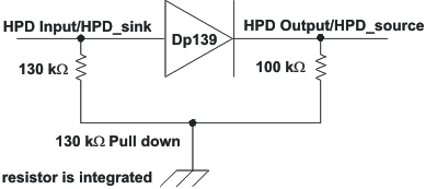 Figure 1. HPD Test Circuit (HPDINV = LOW)
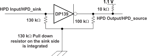 Figure 2. HPD Test Circuit (VOH = 1.1),
 HPDINV = HIGH
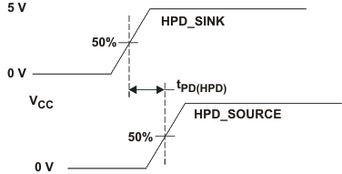 Figure 3. HPD Timing Diagram (HPDINV = LOW)
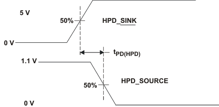 Figure 4. HPD Timing Diagram (HPDINV = HIGH)
6.10 Switching Characteristics (Aux / I2C Pins)
over recommended operating conditions (unless otherwise noted)| PARAMETER | TEST CONDITIONS | MIN | TYP | MAX | UNIT | |
|---|---|---|---|---|---|---|
| tPLH1 | Propagation delay time, low to high | Source to Sink | 204 | 600 | ns | |
| tPHL1 | Propagation delay time, high to low | Source to Sink | 35 | 200 | ns | |
| tPLH2 | Propagation delay time, low to high | Sink to Source | 80 | 251 | ns | |
| tPHL2 | Propagation delay time, high to low | Sink to Source | 35 | 200 | ns | |
| tf1 | Output signal fall time | Sink Side | 20 | 72 | ns | |
| tf2 | Output signal fall time | Source Side | 20 | 72 | ns | |
| fSCL | SCL clock frequency for internal register | Source Side | 100 | kHz | ||
| tW(L) | Clock LOW period for I2C register | Source Side | 4.7 | μs | ||
| tW(H) | Clock HIGH period for internal register | Source Side | 4.0 | μs | ||
| tSU1 | Internal register setup time, SDA to SCL | Source Side | 250 | ns | ||
| th(1) | Internal register hold time, SCL to SDA | Source Side | 0 | μs | ||
| T(buf) | Internal register bus free time between STOP and START | Source Side | 4.7 | μs | ||
| tsu(2) | Internal register setup time, SCL to START | Source Side | 4.7 | μs | ||
| th(2) | Internal register hold time, START to SCL | Source Side | 4.0 | μs | ||
| tsu(3) | Internal register hold time, SCL to STOP | Source Side | 4.0 | μs | ||
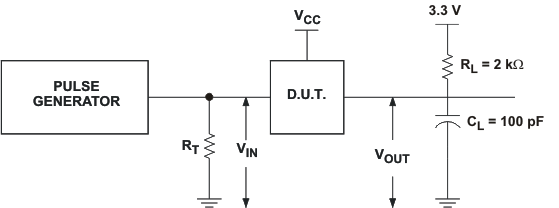 Figure 5. Source Side Test Circuit (SCL_SOURCE, SDA_SOURCE)
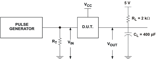 Figure 6. Sink Side Test Circuit (SCL_SINK,SDA_SINK)
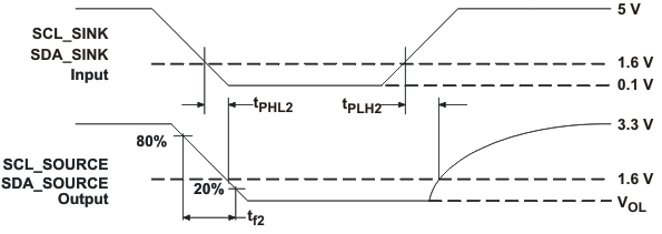 Figure 7. Source Side Output AC Measurements
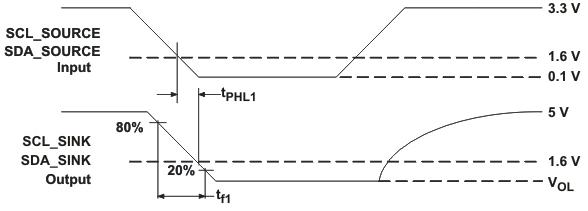 Figure 8. Sink Side Output AC Measurements
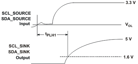 Figure 9. Sink Side Output AC Measurements Continued
6.11 Switching Characteristics (TMDS and Main Link Pins)
over recommended operating conditions (unless otherwise noted)| PARAMETER | TEST CONDITIONS | MIN | TYP | MAX | UNIT | |
|---|---|---|---|---|---|---|
| tPLH | Propagation delay time | AVCC=3.3 V, RT = 50 Ω, f = 1MHz, RVsadj = 4.02 kΩ |
250 | 350 | 600 | ps |
| tPHL | Propagation delay time | 250 | 350 | 600 | ps | |
| tR1 | Rise Time (I2C_EN = HI, SRC = Hi-Z) | 60 | 85 | 120 | ps | |
| tF1 | Fall Time (I2C_EN = HI, SRC = Hi-Z) | 60 | 85 | 120 | ps | |
| tR2 | Rise Time (I2C_EN = Low, SRC = Hi-Z) | 115 | 150 | ps | ||
| tF2 | Fall Time (I2C_EN = Low, SRC = Hi-Z) | 115 | 150 | ps | ||
| tR3 | Rise Time (I2C_EN = HI, SRC = HI) | 150 | 180 | ps | ||
| tF3 | Fall Time (I2C_EN = HI, SRC = HI) | 150 | 180 | ps | ||
| tR4 | Rise Time (I2C_EN = HI, SRC = Low) | 115 | 150 | ps | ||
| tF4 | Fall Time (I2C_EN = HI, SRC = Low) | 115 | 150 | ps | ||
| tR5 | Rise Time (I2C_EN = Low, SRC = HI) | 175 | 220 | ps | ||
| tF5 | Fall Time (I2C_EN = Low, SRC = HI) | 175 | 220 | ps | ||
| tR6 | Rise Time (I2C_EN = Low, SRC = Low) | 150 | 180 | ps | ||
| tF6 | Fall Time (I2C_EN = Low, SRC = Low) | 150 | 180 | ps | ||
| tSK(P) | Pulse skew | 8 | 15 | ps | ||
| tSK(D) | Intra-pair skew | 20 | 65 | ps | ||
| tSK(O) | Inter-pair skew | 20 | 100 | ps | ||
| tJITD(PP) | Peak-to-peak output residual data jitter | AVCC = 3.3 V, RT = 50Ω, dR = 3Gbps, TMDS output slew rate (default). RVsadj = 4.02 kΩ (refer to Figure 13) |
14 | 50 | ps | |
| tJITC(PP) | Peak-to-peak output residual clock jitter | AVCC = 3.3 V, RT = 50Ω, f = 300 MHz
TMDS output slew rate (default). RVsadj= 4.02 kΩ (refer to Figure 13) |
8 | 30 | ps | |
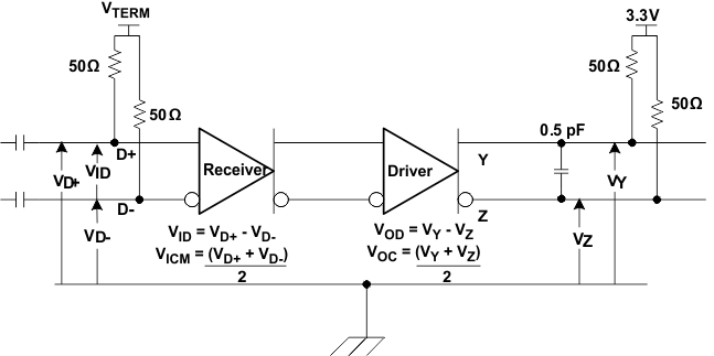 Figure 10. TMDS Main Link Test Circuit
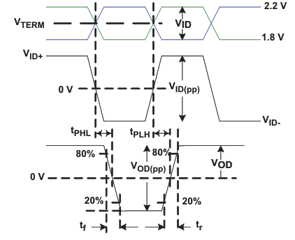 Figure 11. TMDS Main Link Timing Measurements
 Figure 12. TMDS Main Link Common Mode Measurements
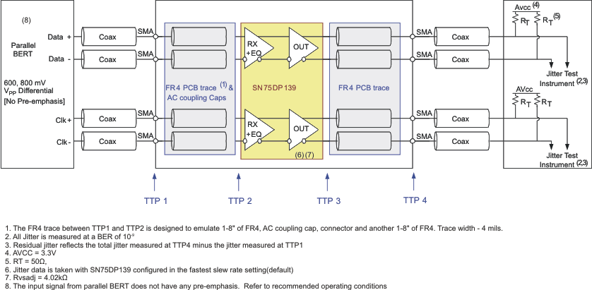 Figure 13. TMDS Jitter Measurements
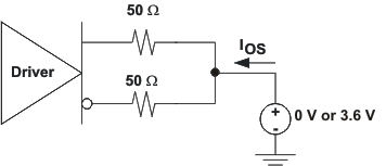 Figure 14. TMDS Main Link Short Circuit Output Circuit
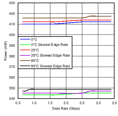
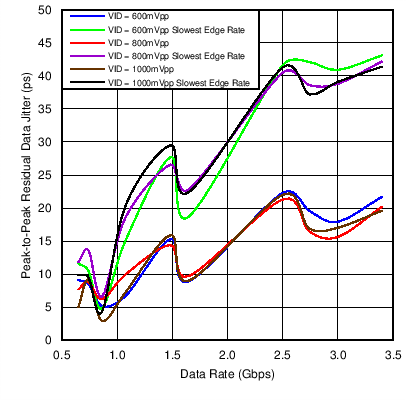
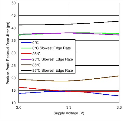
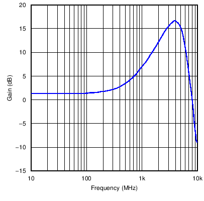
6.12 Typical Characteristics
AVCC = 3.3 V, RT = 50 Ω