SLAS513C February 2007 – December 2014 TLV320AIC3105
PRODUCTION DATA.
- 1 Features
- 2 Applications
- 3 Description
- 4 Revision History
- 5 Description (Continued)
- 6 Related Devices
- 7 Pin Configuration and Functions
- 8 Specifications
- 9 Parameter Measurement Information
-
10Detailed Description
- 10.1 Overview
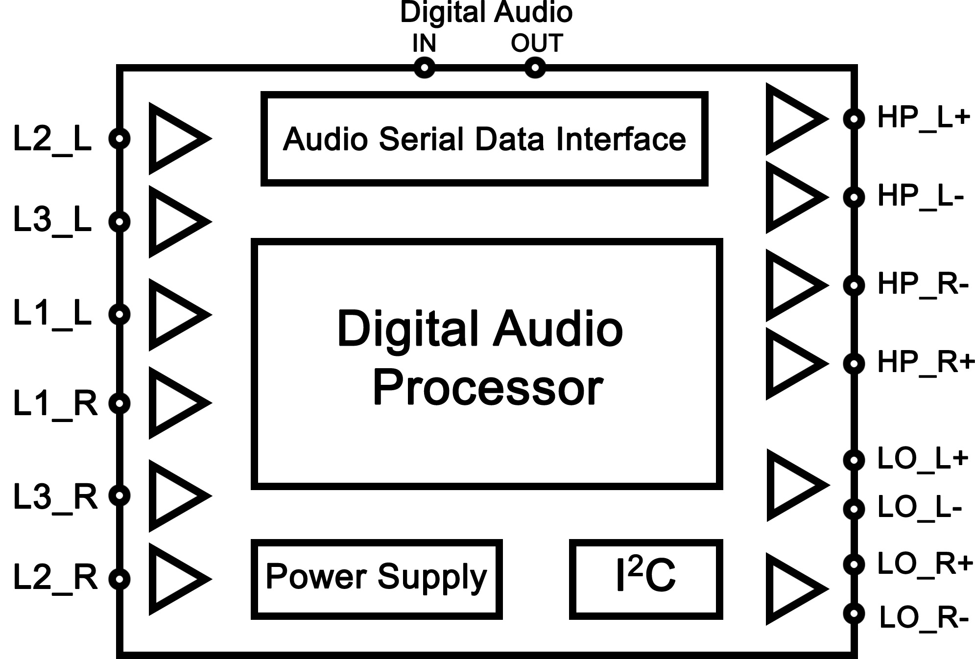
- 10.2 Functional Block Diagram
- 10.3
Feature Description
- 10.3.1 Hardware Reset
- 10.3.2 Digital Control Serial Interface
- 10.3.3 Audio Data Converters
- 10.3.4 Audio Analog Inputs
- 10.3.5 Analog Fully Differential Line Output Drivers
- 10.3.6 Analog High-Power Output Drivers
- 10.3.7 Input Impedance and VCM Control
- 10.3.8 MICBIAS Generation
- 10.3.9 Short-Circuit Output Protection
- 10.3.10 Jack and Headset Detection
- 10.4 Device Functional Modes
- 10.5 Programming
- 10.6 Register Maps
- 11Application and Implementation
- 12Power Supply Recommendations
- 13Layout
- 14Device and Documentation Support
- 15Mechanical, Packaging, and Orderable Information
パッケージ・オプション
メカニカル・データ(パッケージ|ピン)
- RHB|32
サーマルパッド・メカニカル・データ
- RHB|32
発注情報
1 Features
-
Stereo Audio DAC
- 102-dBA Signal-to-Noise Ratio
- 16/20/24/32-Bit Data
- Supports Rates From 8 kHz to 96 kHz
- 3D/Bass/Treble/EQ/De-Emphasis Effects
- Flexible Power Saving Modes and Performance are Available
- Stereo Audio ADC
- 92-dBA Signal-to-Noise Ratio
- Supports Rates From 8 kHz to 96 kHz
- Digital Signal Processing and Noise Filtering Available During Record
- Six Audio Input Pins
- Six Stereo Single-Ended Inputs
- Six Audio Output Drivers
- Stereo Fully Differential or Single-Ended Headphone Drivers
- Fully Differential Stereo Line Outputs
- Low Power: 14-mW Stereo 48-kHz Playback With 3.3-V Analog Supply
- Ultralow-Power Mode with Passive Analog Bypass
- Programmable Input/Output Analog Gains
- Automatic Gain Control (AGC) for Record
- Programmable Microphone Bias Level
- Programmable PLL for Flexible Clock Generation
- I2C Control Bus
- Audio Serial Data Bus Supports I2S, Left/Right-Justified, DSP, and TDM Modes
- Extensive Modular Power Control
- Power Supplies:
- Analog: 2.7 V–3.6 V.
- Digital Core: 1.525 V–1.95 V
- Digital I/O: 1.1 V–3.6 V
- Package: 5-mm × 5-mm 32-Pin VQFN
2 Applications
- Digital Cameras
- Smart Cellular Phones
3 Description
The TLV320AIC3105 is a low-power stereo audio codec with multiple single-ended inputs and a stereo headphone amplifier. The output stages are programmable in single-ended or fully differential configurations. Extensive register-based power control is included, enabling stereo 48-kHz DAC playback as low as 14 mW from a 3.3-V analog supply, making it ideal for portable battery-powered audio and telephony applications.
The record path of the TLV320AIC3105 contains integrated microphone bias, digitally controlled stereo microphone preamplifier, and automatic gain control (AGC), with mix/mux capability among the multiple analog inputs. Programmable filters are available during record which can remove audible noise that can occur during optical zooming in digital cameras. The playback path includes mix/mux capability from the stereo DAC and selected inputs, through programmable volume controls, to the various outputs.
Device Information(1)
| PART NUMBER | PACKAGE | BODY SIZE (NOM) |
|---|---|---|
| TLV320AIC3105 | VQFN (32) | 5.00 mm × 5.00 mm |
- For all available packages, see the orderable addendum at the end of the datasheet.
Simplified Diagram