SPRS614F March 2011 – March 2015 TMS320DM8165 , TMS320DM8167 , TMS320DM8168
PRODUCTION DATA.
- 1 Device Overview
- 2 Revision History
- 3 Device Comparison
-
4 Terminal Configuration and Functions
- 4.1 Pin Assignments
- 4.2
Terminal Functions
- 4.2.1 Boot Configuration
- 4.2.2 DDR2 and DDR3 Memory Controller Signals
- 4.2.3 Ethernet Media Access Controller (EMAC) Signals
- 4.2.4 General-Purpose Input/Output (GPIO) Signals
- 4.2.5 General-Purpose Memory Controller (GPMC) Signals
- 4.2.6 High-Definition Multimedia Interface (HDMI) Signals
- 4.2.7 Inter-Integrated Circuit (I2C) Signals
- 4.2.8 Multichannel Audio Serial Port Signals
- 4.2.9 Multichannel Buffered Serial Port Signals
- 4.2.10 Oscillator/Phase-Locked Loop (PLL) Signals
- 4.2.11 Peripheral Component Interconnect Express (PCIe) Signals
- 4.2.12 Reset, Interrupts, and JTAG Interface Signals
- 4.2.13 Secure Digital/Secure Digital Input Output (SD/SDIO) Signals
- 4.2.14 Serial ATA Signals
- 4.2.15 Serial Peripheral Digital Interconnect Format (SPI) Signals
- 4.2.16 Timer Signals
- 4.2.17 Universal Asynchronous Receiver/Transmitter (UART) Signals
- 4.2.18 Universal Serial Bus (USB) Signals
- 4.2.19 Video Input Signals
- 4.2.20 Digital Video Output Signals
- 4.2.21 Analog Video Output Signals
- 4.2.22 Reserved Pins
- 4.2.23 Supply Voltages
- 4.2.24 Ground Pins (VSS)
- 5 Specifications
- 6 Device Configurations
- 7 System Interconnect
-
8 Power, Reset, Clocking, and Interrupts
- 8.1 Power Supplies
- 8.2
Reset
- 8.2.1 System-Level Reset Sources
- 8.2.2 Power-On Reset (POR pin)
- 8.2.3 External Warm Reset (RESET pin)
- 8.2.4 Emulation Warm Reset
- 8.2.5 Watchdog Reset
- 8.2.6 Software Global Cold Reset
- 8.2.7 Software Global Warm Reset
- 8.2.8 Test Reset (TRST pin)
- 8.2.9 Local Reset
- 8.2.10 Reset Priority
- 8.2.11 Reset Status Register
- 8.2.12 PCIe Reset Isolation
- 8.2.13 RSTOUT
- 8.2.14 Effect of Reset on Emulation and Trace
- 8.2.15 Reset During Power Domain Switching
- 8.2.16 Pin Behaviors at Reset
- 8.2.17 Reset Electrical Data and Timing
- 8.3 Clocking
- 8.4 Interrupts
-
9 Peripheral Information and Timings
- 9.1 Parameter Information
- 9.2 Recommended Clock and Control Signal Transition Behavior
- 9.3
DDR2 and DDR3 Memory Controller
- 9.3.1
DDR2 Routing Specifications
- 9.3.1.1 Board Designs
- 9.3.1.2
DDR2 Interface
- 9.3.1.2.1 DDR2 Interface Schematic
- 9.3.1.2.2 Compatible JEDEC DDR2 Devices
- 9.3.1.2.3 PCB Stackup
- 9.3.1.2.4 Placement
- 9.3.1.2.5 DDR2 Keepout Region
- 9.3.1.2.6 Bulk Bypass Capacitors
- 9.3.1.2.7 High-Speed Bypass Capacitors
- 9.3.1.2.8 Net Classes
- 9.3.1.2.9 DDR2 Signal Termination
- 9.3.1.2.10 VREFSSTL_DDR Routing
- 9.3.1.3 DDR2 CK and ADDR_CTRL Routing
- 9.3.2
DDR3 Routing Specifications
- 9.3.2.1 Board Designs
- 9.3.2.2 DDR3 Device Combinations
- 9.3.2.3 DDR3 Interface Schematic
- 9.3.2.4 Compatible JEDEC DDR3 Devices
- 9.3.2.5 PCB Stackup
- 9.3.2.6 Placement
- 9.3.2.7 DDR3 Keepout Region
- 9.3.2.8 Bulk Bypass Capacitors
- 9.3.2.9 High-Speed Bypass Capacitors
- 9.3.2.10 Net Classes
- 9.3.2.11 DDR3 Signal Termination
- 9.3.2.12 VREFSSTL_DDR Routing
- 9.3.2.13 VTT
- 9.3.2.14 CK and ADDR_CTRL Topologies and Routing Definition
- 9.3.2.15 Data Topologies and Routing Definition
- 9.3.2.16 Routing Specification
- 9.3.3 DDR2 and DDR3 Memory Controller Register Descriptions
- 9.3.4 DDR2 and DDR3 PHY Register Descriptions
- 9.3.5 DDR2 and DDR3 Memory Controller Electrical Data and Timing
- 9.3.1
DDR2 Routing Specifications
- 9.4 Emulation Features and Capability
- 9.5 Enhanced Direct Memory Access (EDMA) Controller
- 9.6 Ethernet Media Access Controller (EMAC)
- 9.7 General-Purpose Input and Output (GPIO)
- 9.8 General-Purpose Memory Controller (GPMC) and Error Locator Module (ELM)
- 9.9 High-Definition Multimedia Interface (HDMI)
- 9.10 High-Definition Video Processing Subsystem (HDVPSS)
- 9.11 Inter-Integrated Circuit (I2C)
- 9.12 Multichannel Audio Serial Port (McASP)
- 9.13 Multichannel Buffered Serial Port (McBSP)
- 9.14 Peripheral Component Interconnect Express (PCIe)
- 9.15 Real-Time Clock (RTC)
- 9.16 Secure Digital and Secure Digital Input Output (SD and SDIO)
- 9.17 Serial ATA Controller (SATA)
- 9.18 Serial Peripheral Interface (SPI)
- 9.19 Timers
- 9.20 Universal Asynchronous Receiver and Transmitter (UART)
- 9.21 Universal Serial Bus (USB2.0)
- 10Device and Documentation Support
- 11Mechanical Packaging and Orderable Information
パッケージ・オプション
デバイスごとのパッケージ図は、PDF版データシートをご参照ください。
メカニカル・データ(パッケージ|ピン)
- CYG|1031
サーマルパッド・メカニカル・データ
発注情報
9 Peripheral Information and Timings
9.1 Parameter Information
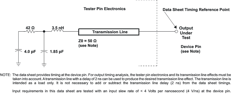 Figure 9-1 Test Load Circuit for AC Timing Measurements
The load capacitance value stated is only for characterization and measurement of AC timing signals. This load capacitance value does not indicate the maximum load the device is capable of driving.
9.1.1 1.8-V and 3.3-V Signal Transition Levels
All input and output timing parameters are referenced to Vref for both "0" and "1" logic levels. For 3.3-V IO, Vref = 1.5 V. For 1.8-V IO, Vref = 0.9 V.
 Figure 9-2 Input and Output Voltage Reference Levels for AC Timing Measurements
All rise and fall transition timing parameters are referenced to VIL MAX and VIH MIN for input clocks, VOL MAX and VOH MIN for output clocks.
 Figure 9-3 Rise and Fall Transition Time Voltage Reference Levels
9.1.2 3.3-V Signal Transition Rates
All timings are tested with an input edge rate of 4 volts per nanosecond (4 V per ns).
9.1.3 Timing Parameters and Board Routing Analysis
The timing parameter values specified in this data manual do not include delays by board routings. As a good board design practice, such delays must always be taken into account. Timing values may be adjusted by increasing or decreasing such delays. TI recommends utilizing the available IO buffer information specification (IBIS) models to analyze the timing characteristics correctly. To properly use IBIS models to attain accurate timing analysis for a given system, see the Using IBIS Models for Timing Analysis application report (literature number SPRA839). If needed, external logic hardware such as buffers may be used to compensate any timing differences.
For the DDR2 and DDR3, PCIe, SATA, USB, and HDMI interfaces, IBIS models are not used for timing specification. TI provides, in this document, a PCB routing rule solution for each interface that describes the routing rules used to ensure the interface timings are met. Video DAC guidelines (Section 9.10.2) are also included to discuss important layout considerations.
9.2 Recommended Clock and Control Signal Transition Behavior
All clocks and control signals must transition between VIH and VIL (or between VIL and VIH) in a monotonic manner.
9.3 DDR2 and DDR3 Memory Controller
The device has a dedicated interface to DDR3 and DDR2 SDRAM. It supports JEDEC standard-compliant DDR2 and DDR3 SDRAM devices with the following features:
- 16-bit or 32-bit data path to external SDRAM memory
- Memory device capacity: 64Mb, 128Mb, 256Mb, 512Mb, 1Gb, 2Gb and 4Gb (x16-bit only) devices
- Support for two independent chip selects, with their corresponding register sets, and independent page tracking
- Two interfaces with associated DDR2 and DDR3 PHYs
- Dynamic memory manager allows for interleaving of data between the two DDR interfaces.
For details on the DDR2 and DDR3 Memory Controller, see the DDR2 and DDR3 Memory Controller chapter in the TMS320DM816x DaVinci Digital Media Processors Technical Reference Manual (literature number SPRUGX8).
9.3.1 DDR2 Routing Specifications
9.3.1.1 Board Designs
TI only supports board designs that follow the specifications outlined in this document. The switching characteristics and the timing diagram for the DDR2 memory controller are shown in Table 9-1 and Figure 9-4.
Table 9-1 Switching Characteristics Over Recommended Operating Conditions for DDR2 Memory Controller
| NO. | PARAMETER | -1G | UNIT | ||
|---|---|---|---|---|---|
| MIN | MAX | ||||
| 1 | tc(DDR_CLK) | Cycle time, DDR_CLK | 2.5 | 8 | ns |
 Figure 9-4 DDR2 Memory Controller Clock Timing
9.3.1.2 DDR2 Interface
This section provides the timing specification for the DDR2 interface as a PCB design and manufacturing specification. The design rules constrain PCB trace length, PCB trace skew, signal integrity, cross-talk, and signal timing. These rules, when followed, result in a reliable DDR2 memory system without the need for a complex timing closure process. For more information regarding the guidelines for using this DDR2 specification, see Understanding TI’s PCB Routing Rule-Based DDR2 Timing Specification Application Report (SPRAAV0).
9.3.1.2.1 DDR2 Interface Schematic
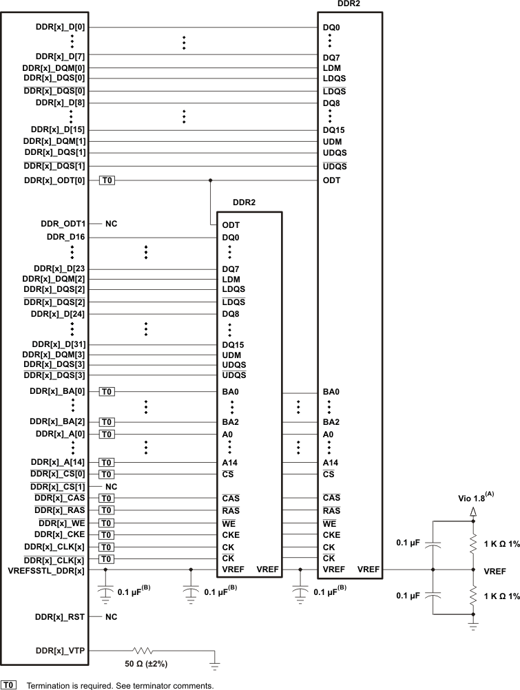
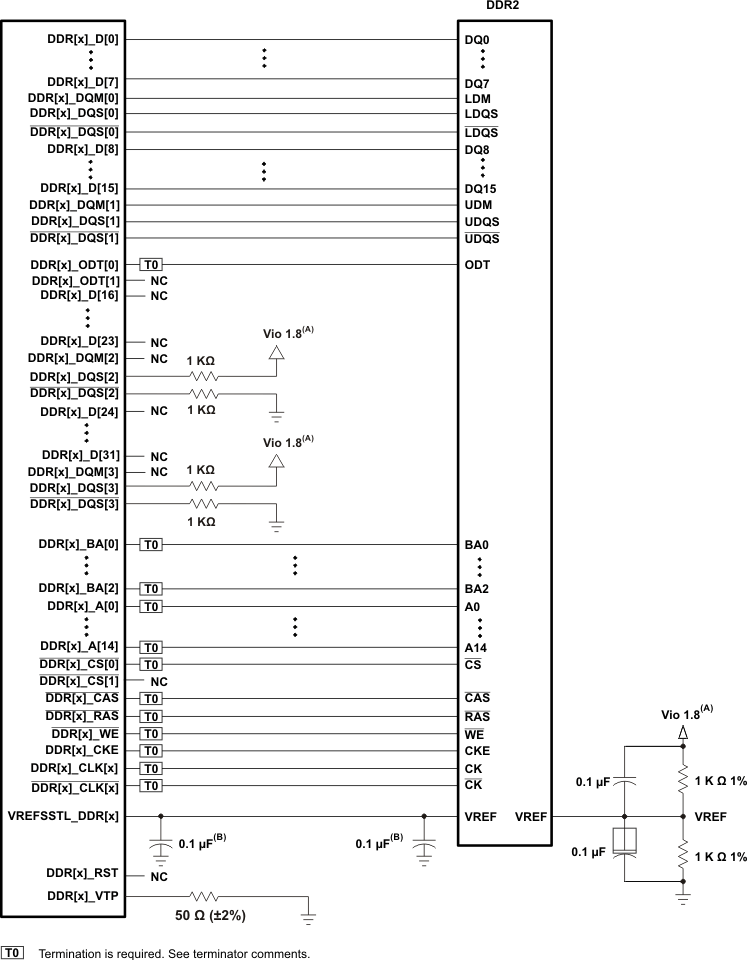
Figure 9-5 shows the DDR2 interface schematic for a x32 DDR2 memory system. In Figure 9-6 the x16 DDR2 system schematic is identical except that the high-word DDR2 device is deleted.
When not using a DDR2 interface, the proper method of handling the unused pins is to tie off the DQS pins by pulling the non-inverting DQS pin to the DDR_1V8 supply via a 1k-Ω resistor and pulling the inverting DQS pin to ground via a 1k-Ω resistor. This needs to be done for each byte not used. Also, include the 50-Ω pulldown for DDR[x]_VTP. All other DDR interface pins can be left unconnected. Note that the supported modes for use of the DDR EMIF are 32 bits wide, 16 bits wide, or not used.
9.3.1.2.2 Compatible JEDEC DDR2 Devices
Table 9-2 shows the parameters of the JEDEC DDR2 devices that are compatible with this interface. Generally, the DDR2 interface is compatible with x16 DDR2-800 speed grade DDR2 devices.
Table 9-2 Compatible JEDEC DDR2 Devices
| NO. | PARAMETER | MIN | MAX | UNIT |
|---|---|---|---|---|
| 1 | JEDEC DDR2 device speed grade(1) | DDR2-800 | ||
| 2 | JEDEC DDR2 device bit width | x16 | x16 | Bits |
| 3 | JEDEC DDR2 device count(2) | 1 | 2 | Devices |
| 4 | JEDEC DDR2 device ball count(3) | 84 | 92 | Balls |
9.3.1.2.3 PCB Stackup
The minimum stackup required for routing the DM816x device is a six-layer stackup as shown in Table 9-3. Additional layers may be added to the PCB stackup to accommodate other circuitry or to reduce the size of the PCB footprint.
Table 9-3 Minimum PCB Stackup
| LAYER | TYPE | DESCRIPTION |
|---|---|---|
| 1 | Signal | Top routing mostly horizontal |
| 2 | Plane | Ground |
| 3 | Plane | Power |
| 4 | Signal | Internal routing |
| 5 | Plane | Ground |
| 6 | Signal | Bottom routing mostly vertical |
Complete stackup specifications are provided in Table 9-4.
Table 9-4 PCB Stackup Specifications
| NO. | PARAMETER | MIN | TYP | MAX | UNIT |
|---|---|---|---|---|---|
| 1 | PCB routing and plane layers | 6 | |||
| 2 | Signal routing layers | 3 | |||
| 3 | Full ground layers under DDR2 routing region | 2 | |||
| 4 | Number of ground plane cuts allowed within DDR routing region | 0 | |||
| 5 | Number of ground reference planes required for each DDR2 routing layer | 1 | |||
| 6 | Number of layers between DDR2 routing layer and reference ground plane | 0 | |||
| 7 | PCB routing feature size | 4 | Mils | ||
| 8 | PCB trace width, w | 4 | Mils | ||
| 9 | PCB BGA escape via pad size(1) | 18 | 20 | Mils | |
| 10 | PCB BGA escape via hole size(1) | 10 | Mils | ||
| 11 | Processor BGA pad size | 0.3 | mm | ||
| 12 | DDR2 device BGA pad size(2) | ||||
| 13 | Single-ended impedance, Zo | 50 | 75 | Ω | |
| 14 | Impedance control(3) | Z-5 | Z | Z+5 | Ω |
9.3.1.2.4 Placement
Figure 9-7 shows the required placement for the processor as well as the DDR2 devices. The dimensions for this figure are defined in Table 9-5. The placement does not restrict the side of the PCB on which the devices are mounted. The ultimate purpose of the placement is to limit the maximum trace lengths and allow for proper routing space. For a 16-bit DDR memory system, the high-word DDR2 device is omitted from the placement.
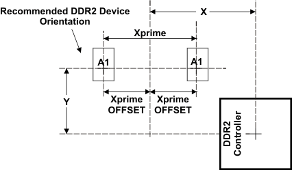 Figure 9-7 DM816x Device and DDR2 Device Placement
Table 9-5 Placement Specifications
| NO. | PARAMETER | MIN | MAX | UNIT |
|---|---|---|---|---|
| 1 | X + Y(1)(2) | 1660 | Mils | |
| 2 | X'(1)(2) | 1280 | Mils | |
| 3 | X' Offset(1)(2)(3) | 650 | Mils | |
| 4 | DDR2 keepout region(4) | |||
| 5 | Clearance from non-DDR2 signal to DDR2 keepout region(5) | 4 | w |
9.3.1.2.5 DDR2 Keepout Region
The region of the PCB used for the DDR2 circuitry must be isolated from other signals. The DDR2 keepout region is defined for this purpose and is shown in Figure 9-8. The size of this region varies with the placement and DDR routing. Additional clearances required for the keepout region are shown in Table 9-5.
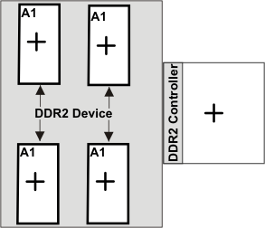 Figure 9-8 DDR2 Keepout Region
NOTE
The region shown in should encompass all the DDR2 circuitry and varies depending on placement. Non-DDR2 signals should not be routed on the DDR signal layers within the DDR2 keepout region. Non-DDR2 signals may be routed in the region, provided t hey are routed on layers separated from DDR2 signal layers by a ground layer. No breaks should be allowed in the reference ground layers in this region. In addition, the 1.8V power plane should cover the entire keepout region. Routes for the two DDR interfaces must be separated by at least 4x; the more separation, the better.
9.3.1.2.6 Bulk Bypass Capacitors
Bulk bypass capacitors are required for moderate speed bypassing of the DDR2 and other circuitry. Table 9-6 contains the minimum numbers and capacitance required for the bulk bypass capacitors. Note that this table only covers the bypass needs of the DDR2 interfaces and DDR2 device. Additional bulk bypass capacitance may be needed for other circuitry.
Table 9-6 Bulk Bypass Capacitors
| No. | Parameter | Min | Max | Unit |
|---|---|---|---|---|
| 1 | DVDD18 bulk bypass capacitor count(1) | 6 | Devices | |
| 2 | DVDD18 bulk bypass total capacitance | 60 | μF | |
| 3 | DDR#1 bulk bypass capacitor count(1) | 1 | Devices | |
| 4 | DDR#1 bulk bypass total capacitance(1) | 10 | μF | |
| 5 | DDR#2 bulk bypass capacitor count(2) | 1 | Devices | |
| 6 | DDR#2 bulk bypass total capacitance(1)(2) | 10 | μF |
9.3.1.2.7 High-Speed Bypass Capacitors
High-speed (HS) bypass capacitors are critical for proper DDR2 interface operation. It is particularly important to minimize the parasitic series inductance of the HS bypass capacitors, processor DDR power, and processor DDR ground connections. Table 9-7 contains the specification for the HS bypass capacitors as well as for the power connections on the PCB.
Table 9-7 High-Speed Bypass Capacitors
| NO. | PARAMETER | MIN | MAX | UNIT |
|---|---|---|---|---|
| 1 | HS bypass capacitor package size(1) | 0402 | 10 Mils | |
| 2 | Distance from HS bypass capacitor to device being bypassed | 250 | Mils | |
| 3 | Number of connection vias for each HS bypass capacitor(2) | 2 | Vias | |
| 4 | Trace length from bypass capacitor contact to connection via | 1 | 30 | Mils |
| 5 | Number of connection vias for each processor power and ground ball | 1 | Vias | |
| 6 | Trace length from processor power and ground ball to connection via | 35 | Mils | |
| 7 | Number of connection vias for each DDR2 device power and ground ball | 1 | Vias | |
| 8 | Trace length from DDR2 device power and ground ball to connection via | 35 | Mils | |
| 9 | DVDD18 HS bypass capacitor count(3)(4) | 40 | Devices | |
| 10 | DVDD18 HS bypass capacitor total capacitance(4) | 2.4 | μF | |
| 11 | DDR device HS bypass capacitor count(3)(5) | 8 | Devices | |
| 12 | DDR device HS bypass capacitor total capacitance(5) | 0.4 | μF |
9.3.1.2.8 Net Classes
Table 9-8 lists the clock net classes for the DDR2 interface. Table 9-9 lists the signal net classes, and associated clock net classes, for the signals in the DDR2 interface. These net classes are used for the termination and routing rules that follow.
Table 9-8 Clock Net Class Definitions
| CLOCK NET CLASS | PROCESSOR PIN NAMES |
|---|---|
| CK | DDR[x]_CLK[x] and DDR[x]_CLK[x] |
| DQS0 | DDR[x]_DQS[0] and DDR[x]_DQS[0] |
| DQS1 | DDR[x]_DQS[1] and DDR[x]_DQS[1] |
| DQS2(1) | DDR[x]_DQS[2] and DDR[x]_DQS[2] |
| DQS3(1) | DDR[x]_DQS[3] and DDR[x]_DQS[3] |
Table 9-9 Signal Net Class Definitions
| SIGNAL NET CLASS | ASSOCIATED CLOCK NET CLASS |
PROCESSOR PIN NAMES |
|---|---|---|
| ADDR_CTRL | CK | DDR[x]_BA[2:0], DDR[x]_A[14:0], DDR[x]_CS[x], DDR[x]_CAS, DDR[x]_RAS, DDR[x]_WE, DDR[x]_CKE, DDR[x]_ODT[x] |
| DQ0 | DQS0 | DDR[x]_D[7:0], DDR[x]_DQM[0] |
| DQ1 | DQS1 | DDR[x]_D[15:8], DDR[x]_DQM[1] |
| DQ2(1) | DQS2 | DDR[x]_D[23:16], DDR[x]_DQM[2] |
| DQ3(1) | DQS3 | DDR[x]_D[31:24], DDR[x]_DQM[3] |
9.3.1.2.9 DDR2 Signal Termination
Signal terminators are required in CK and ADDR_CTRL net classes. Serial terminators may be used on data lines to reduce EMI risk; however, serial terminations are the only type permitted. ODT's are integrated on the data byte net classes. They should be enabled to ensure signal integrity.Table 9-10 shows the specifications for the series terminators.
Table 9-10 DDR2 Signal Terminations
| NO. | PARAMETER | MIN | TYP | MAX | UNIT |
|---|---|---|---|---|---|
| 1 | CK net class(1)(4) | 0 | 10 | Ω | |
| 2 | ADDR_CTRL net class(1)(2)(3)(4) | 0 | 22 | Zo | Ω |
| 3 | Data byte net classes (DQS0-DQS3, DQ0-DQ3)(5) | 0 | 0 | Ω |
9.3.1.2.10 VREFSSTL_DDR Routing
VREFSSTL_DDR is used as a reference by the input buffers of the DDR2 memories as well as the processor. VREF is intended to be half the DDR2 power supply voltage and should be created using a resistive divider as shown in Figure 9-6. Other methods of creating VREF are not recommended. Figure 9-9 shows the layout guidelines for VREF.
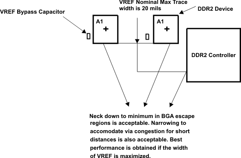 Figure 9-9 VREF Routing and Topology
9.3.1.3 DDR2 CK and ADDR_CTRL Routing
Figure 9-10 shows the topology of the routing for the CK and ADDR_CTRL net classes. The route is a balanced T as it is intended that the length of segments B and C be equal. In addition, the length of A (A'+A'') should be maximized.
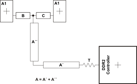 Figure 9-10 CK and ADDR_CTRL Routing and Topology
Table 9-11 CK and ADDR_CTRL Routing Specification (1)
| NO. | PARAMETER | MIN | TYP | MAX | UNIT |
|---|---|---|---|---|---|
| 1 | Center-to-center CK-CK spacing | 2w | |||
| 2 | CK and CK skew(1) | 25 | Mils | ||
| 3 | CK B-to-C skew length mismatch | 25 | Mils | ||
| 4 | Center-to-center CK to other DDR2 trace spacing(2) | 4w | |||
| 5 | CK and ADDR_CTRL nominal trace length(3) | CACLM-50 | CACLM | CACLM+50 | Mils |
| 6 | ADDR_CTRL-to-CK skew length mismatch | 100 | Mils | ||
| 7 | ADDR_CTRL-to-ADDR_CTRL skew length mismatch | 100 | Mils | ||
| 8 | Center-to-center ADDR_CTRL to other DDR2 trace spacing(2) | 4w | |||
| 9 | Center-to-center ADDR_CTRL to other ADDR_CTRL trace spacing(2) | 3w | |||
| 10 | ADDR_CTRL B-to-C skew length mismatch | 100 | Mils |
Figure 9-11 shows the topology and routing for the DQS and DQ net classes; the routes are point to point. Skew matching across bytes is not needed nor recommended.
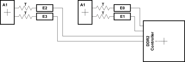 Figure 9-11 DQS and DQ Routing and Toplogy
Table 9-12 DQS and DQ Routing Specification
| NO. | PARAMETER | MIN | TYP | MAX | UNIT |
|---|---|---|---|---|---|
| 1 | Center-to-center DQS-DQSn spacing in E0|E1|E2|E3 | 2w | |||
| 2 | DQS-DQSn skew in E0|E1|E2|E3 | 25 | Mils | ||
| 3 | Center-to-center DQS to other DDR2 trace spacing(1) | 4w | |||
| 4 | DQS and DQ nominal trace length (2)(3)(4) | DQLM-50 | DQLM | DQLM+50 | Mils |
| 5 | DQ-to-DQS skew length mismatch(2)(3)(4) | 100 | Mils | ||
| 6 | DQ-to-DQ skew length mismatch(2)(3)(4) | 100 | Mils | ||
| 7 | DQ-to-DQ and DQS via count mismatch(2)(3)(4) | 1 | Vias | ||
| 8 | Center-to-center DQ to other DDR2 trace spacing(1)(5) | 4w | |||
| 9 | Center-to-center DQ to other DQ trace spacing(1)(6)(7) | 3w | |||
| 10 | DQ and DQS E skew length mismatch(2)(3)(4) | 100 | Mils |
9.3.2 DDR3 Routing Specifications
9.3.2.1 Board Designs
TI only supports board designs utilizing DDR3 memory that follow the specifications in this document. The switching characteristics and timing diagram for the DDR3 memory controller are shown in Table 9-13 and Figure 9-12.
Table 9-13 Switching Characteristics Over Recommended Operating Conditions for DDR3 Memory Controller
| NO. | PARAMETER | -1G | UNIT | ||
|---|---|---|---|---|---|
| MIN | MAX | ||||
| 1 | tc(DDR_CLK) | Cycle time, DDR_CLK | 1.25 | 3.3(1) | ns |
 Figure 9-12 DDR3 Memory Controller Clock Timing
9.3.2.1.1 DDR3 versus DDR2
This specification only covers TMS320DM816x processor PCB designs that utilize DDR3 memory. Designs using DDR2 memory should use the PCB design specifications for DDR2 memory in Section 9.3.1. While similar, the two memory systems have different requirements. It is currently not possible to design one PCB that covers both DDR2 and DDR3.
9.3.2.2 DDR3 Device Combinations
Since there are several possible combinations of device counts and single- or dual-side mounting, Table 9-14 summarizes the supported device configurations.
Table 9-14 Supported DDR3 Device Combinations(1)
| NUMBER OF DDR3 DEVICES | DDR3 DEVICE WIDTH (BITS) | MIRRORED? | DDR3 EMIF WIDTH (BITS) |
|---|---|---|---|
| 1 | 16 | N | 16 |
| 2 | 8 | Y(2) | 16 |
| 2 | 16 | N | 32 |
| 2 | 16 | Y(2) | 32 |
| 4 | 8 | N | 32 |
| 4 | 8 | Y(3) | 32 |
9.3.2.2.1 DDR3 EMIFs
The processor contains two separate DDR3 EMIFs. This specification covers one of these EMIFs (DDR[0]) and, thus, needs to be implemented twice, once for each EMIF. The PCB layout generally turns out to be a semi-mirror with DDR[1] being a flipped version of DDR[0]; the only exception being the DDR3 devices themselves are not flipped unless mounted on opposite sides of the PCB. Requirements are identical between the two EMIFs.
9.3.2.3 DDR3 Interface Schematic
9.3.2.3.1 32-Bit DDR3 Interface
The DDR3 interface schematic varies, depending upon the width of the DDR3 devices used and the width of the bus used (16 or 32 bits). General connectivity is straightforward and very similar. 16-bit DDR devices look like two 8-bit devices. Figure 9-13 and Figure 9-14 show the schematic connections for 32-bit interfaces using x16 devices.
9.3.2.3.2 16-Bit DDR3 Interface
Note that the 16-bit wide interface schematic is practically identical to the 32-bit interface (see Figure 9-13 and Figure 9-14); only the high-word DDR memories are removed and the unused DQS inputs are tied off. The processor DDR[x]_DQS[2] and DDR[x]_DQS[3] pins should be pulled to the DDR supply via 1-kΩ resistors. Similarly, the DDR[x]_DQS[2] and DDR[x]_DQS[3] pins should be pulled to ground via 1-kΩ resistors.
When not using a DDR interface, the proper method of handling the unused pins is to tie off the DQS pins by pulling the non-inverting DQS pin to the DDR_1V5 supply via a 1k-Ω resistor and pulling the inverting DQSn pin to ground via a 1k-Ω resistor. This needs to be done for each byte not used. Also, include the 50-Ω pulldown for DDR[x]_VTP. All other DDR interface pins can be left unconnected. Note that the supported modes for use of the DDR EMIF are 32 bits wide, 16 bits wide, or not used.
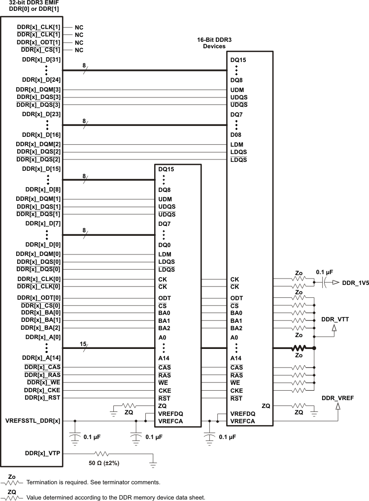 Figure 9-13 32-Bit, One-Bank DDR3 Interface Schematic Using Two 16-Bit DDR3 Devices
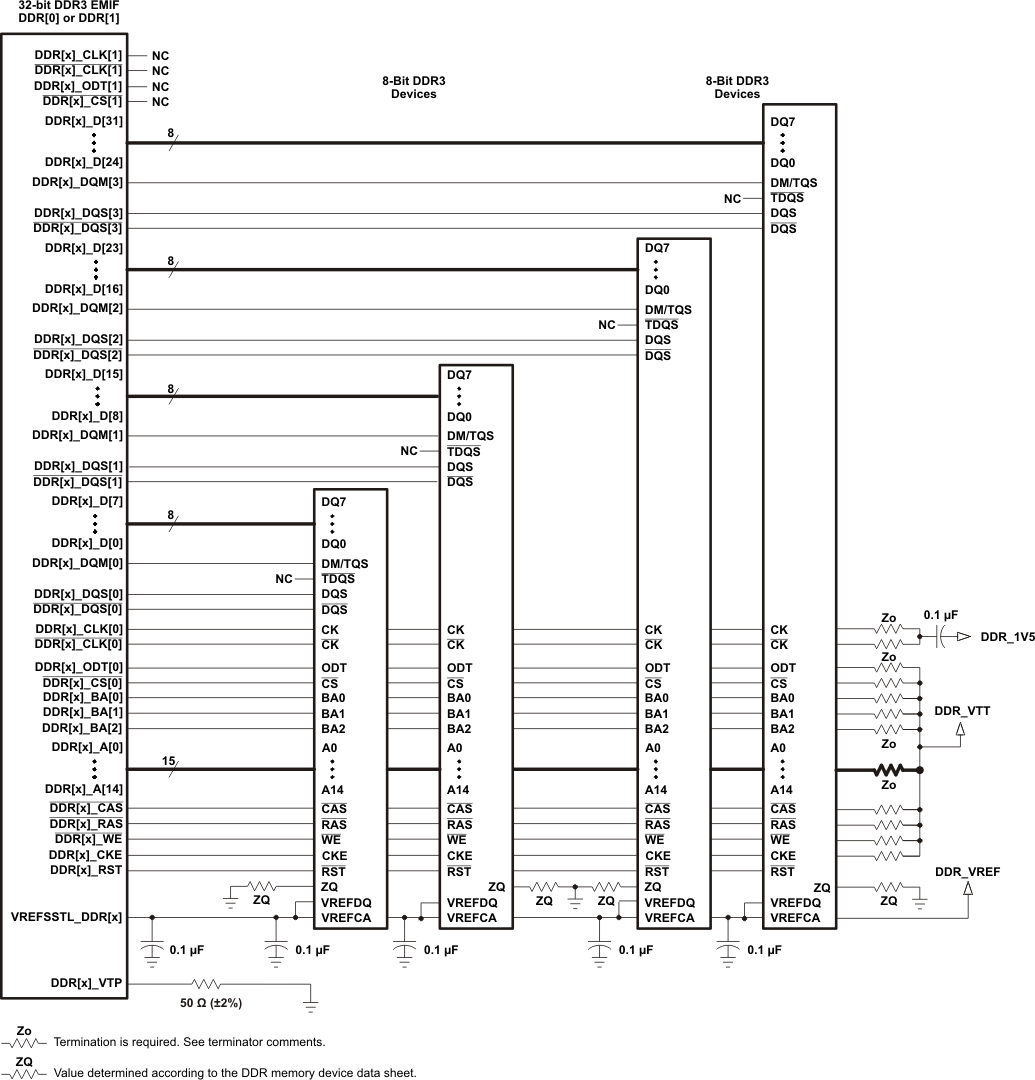 Figure 9-14 32-Bit, One-Bank DDR3 Interface Schematic Using Four 8-Bit DDR3 Devices
9.3.2.4 Compatible JEDEC DDR3 Devices
Table 9-15 shows the parameters of the JEDEC DDR3 devices that are compatible with this interface. Generally, the DDR3 interface is compatible with DDR3-1600 devices in the x8 or x16 widths.
Table 9-15 Compatible JEDEC DDR3 Devices
| NO. | PARAMETER | MIN | MAX | UNIT |
|---|---|---|---|---|
| 1 | JEDEC DDR3 device speed grade(1) | DDR3-800 | DDR3-1600 | |
| 2 | JEDEC DDR3 device bit width | x8 | x16 | Bits |
| 3 | JEDEC DDR3 device count(2) | 2 | 8 | Devices |
9.3.2.5 PCB Stackup
The minimum stackup for routing the DDR3 interface is a four-layer stack up as shown in Table 9-16. Additional layers may be added to the PCB stackup to accommodate other circuitry, enhance SI and EMI performance, or to reduce the size of the PCB footprint. A six-layer stackup is shown in Table 9-17. Complete stackup specifications are provided in Table 9-18.
Table 9-16 Minimum PCB Stackup
| LAYER | TYPE | DESCRIPTION |
|---|---|---|
| 1 | Signal | Top routing mostly vertical |
| 2 | Plane | Split power plane |
| 3 | Plane | Full ground plane |
| 4 | Signal | Bottom routing mostly horizontal |
Table 9-17 Six-Layer PCB Stackup Suggestion
| LAYER | TYPE | DESCRIPTION |
|---|---|---|
| 1 | Signal | Top routing mostly vertical |
| 2 | Plane | Ground |
| 3 | Plane | Split power plane |
| 4 | Plane | Split power plane or Internal routing |
| 5 | Plane | Ground |
| 6 | Signal | Bottom routing mostly horizontal |
Table 9-18 PCB Stackup Specifications
| NO. | PARAMETER | MIN | TYP | MAX | UNIT |
|---|---|---|---|---|---|
| 1 | PCB routing and plane layers | 4 | 6 | ||
| 2 | Signal routing layers | 2 | |||
| 3 | Full ground reference layers under DDR3 routing region(1) | 1 | |||
| 4 | Full 1.5-V power reference layers under the DDR3 routing region(1) | 1 | |||
| 5 | Number of reference plane cuts allowed within DDR routing region(2) | 0 | |||
| 6 | Number of layers between DDR3 routing layer and reference plane(3) | 0 | |||
| 7 | PCB routing feature size | 4 | Mils | ||
| 8 | PCB trace width, w | 4 | Mils | ||
| 9 | PCB BGA escape via pad size(4) | 18 | 20 | Mils | |
| 10 | PCB BGA escape via hole size | 10 | Mils | ||
| 11 | Processor BGA pad size | 0.3 | mm | ||
| 12 | DDR3 device BGA pad size(5) | ||||
| 13 | Single-ended impedance, Zo | 50 | 75 | Ω | |
| 14 | Impedance control(6) | Z-5 | Z | Z+5 | Ω |
9.3.2.6 Placement
Figure 9-15 shows the required placement for the processor as well as the DDR3 devices. The dimensions for this figure are defined in Table 9-19. The placement does not restrict the side of the PCB on which the devices are mounted. The ultimate purpose of the placement is to limit the maximum trace lengths and allow for proper routing space. For a 16-bit DDR memory system, the high-word DDR3 devices are omitted from the placement.
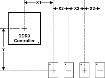 Figure 9-15 Placement Specifications
Table 9-19 Placement Specifications
| NO. | PARAMETER | MIN | MAX | UNIT |
|---|---|---|---|---|
| 1 | X1(1)(2)(3) | 1000 | Mils | |
| 2 | X2(1)(2) | 600 | Mils | |
| 3 | Y Offset(1)(2)(3) | 1500 | Mils | |
| 4 | DDR3 keepout region | |||
| 5 | Clearance from non-DDR3 signal to DDR3 keepout region(4)(5)(6) | 4 | w |
9.3.2.7 DDR3 Keepout Region
The region of the PCB used for DDR3 circuitry must be isolated from other signals. The DDR3 keepout region is defined for this purpose and is shown in Figure 9-16. The size of this region varies with the placement and DDR routing. Additional clearances required for the keepout region are shown in Table 9-19. Non-DDR3 signals should not be routed on the DDR signal layers within the DDR3 keepout region. Non-DDR3 signals may be routed in the region, provided they are routed on layers separated from the DDR signal layers by a ground layer. No breaks should be allowed in the reference ground layers in this region. In addition, the 1.5-V DDR3 power plane should cover the entire keepout region. Also note that the two DDR3 controller's signals should be separated from each other by the specification in Table 9-19, item 5.
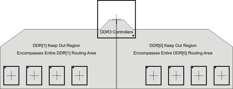 Figure 9-16 DDR3 Keepout Region
9.3.2.8 Bulk Bypass Capacitors
Bulk bypass capacitors are required for moderate speed bypassing of the DDR3 and other circuitry. Table 9-20 contains the minimum numbers and capacitance required for the bulk bypass capacitors. Note that this table only covers the bypass needs of the DDR3 controllers and DDR3 devices. Additional bulk bypass capacitance may be needed for other circuitry. Also note that Table 9-20 is per DDR3 controller; thus, systems using both controllers have to meet the needs of Table 9-20 twice, once for each controller.
Table 9-20 Bulk Bypass Capacitors
| NO. | PARAMETER | MIN | MAX | UNIT |
|---|---|---|---|---|
| 1 | DDR_1V5 bulk bypass capacitor count(1) | 6 | Devices | |
| 2 | DDR_1V5 bulk bypass total capacitance | 140 | μF |
9.3.2.9 High-Speed Bypass Capacitors
High-speed (HS) bypass capacitors are critical for proper DDR3 interface operation. It is particularly important to minimize the parasitic series inductance of the HS bypass capacitors, processor DDR power, and processor DDR ground connections. Table 9-21 contains the specification for the HS bypass capacitors as well as for the power connections on the PCB. Generally speaking, it is good to:
- Fit as many HS bypass capacitors as possible.
- Minimize the distance from the bypass cap to the pins (balls) being bypassed.
- Use the smallest physical sized capacitors possible with the highest capacitance readily available.
- Connect the bypass capacitor pads to their vias using the widest traces possible and using the largest hole size via possible.
- Minimize via sharing. Note the limits on via sharing shown in Table 9-21.
Table 9-21 High-Speed Bypass Capacitors
| NO. | PARAMETER | MIN | TYP | MAX | UNIT |
|---|---|---|---|---|---|
| 1 | HS bypass capacitor package size(1) | 201 | 402 | 10 Mils | |
| 2 | Distance, HS bypass capacitor to processor being bypassed(2)(3)(4) | 400 | Mils | ||
| 3 | Processor DDR_1V5 HS bypass capacitor count | 70 | Devices | ||
| 4 | Processor DDR_1V5 HS bypass capacitor total capacitance | 5 | μF | ||
| 5 | Number of connection vias for each device power and ground ball(5) | Vias | |||
| 6 | Trace length from device power and ground ball to connection via(2) | 35 | 70 | Mils | |
| 7 | Distance, HS bypass capacitor to DDR device being bypassed(6) | 150 | Mils | ||
| 8 | DDR3 device HS bypass capacitor count(7) | 12 | Devices | ||
| 9 | DDR3 device HS bypass capacitor total capacitance(7) | 0.85 | μF | ||
| 10 | Number of connection vias for each HS capacitor(8)(9) | 2 | Vias | ||
| 11 | Trace length from bypass capacitor connect to connection via(2)(9) | 35 | 100 | Mils | |
| 12 | Number of connection vias for each DDR3 device power and ground ball(10) | 1 | Vias | ||
| 13 | Trace length from DDR3 device power and ground ball to connection via(2)(8) | 35 | 60 | Mils |
9.3.2.9.1 Return Current Bypass Capacitors
Use additional bypass capacitors if the return current reference plane changes due to DDR3 signals hopping from one signal layer to another. The bypass capacitor here provides a path for the return current to hop planes along with the signal. As many of these return current bypass capacitors should be used as possible. Since these are returns for signal current, the signal via size may be used for these capacitors.
9.3.2.10 Net Classes
Table 9-22 lists the clock net classes for the DDR3 interface. Table 9-23 lists the signal net classes, and associated clock net classes, for signals in the DDR3 interface. These net classes are used for the termination and routing rules that follow.
Table 9-22 Clock Net Class Definitions
| CLOCK NET CLASS | PROCESSOR PIN NAMES |
|---|---|
| CK | DDR[x]_CLK[x] and DDR[x]_CLK[x] |
| DQS0 | DDR[x]_DQS[0] and DDR[x]_DQS[0] |
| DQS1 | DDR[x]_DQS[1] and DDR[x]_DQS[1] |
| DQS2(1) | DDR[x]_DQS[2] and DDR[x]_DQS[2] |
| DQS3(1) | DDR[x]_DQS[3] and DDR[x]_DQS[3] |
Table 9-23 Signal Net Class Definitions
| SIGNAL NET CLASS | ASSOCIATED CLOCK NET CLASS |
PROCESSOR PIN NAMES |
|---|---|---|
| ADDR_CTRL | CK | DDR[x]_BA[2:0], DDR[x]_A[14:0], DDR[x]_CS[x], DDR[x]_CAS, DDR[x]_RAS, DDR[x]_WE, DDR[x]_CKE, DDR[x]_ODT[x] |
| DQ0 | DQS0 | DDR[x]_D[7:0], DDR[x]_DQM[0] |
| DQ1 | DQS1 | DDR[x]_D[15:8], DDR[x]_DQM[1] |
| DQ2(1) | DQS2 | DDR[x]_D[23:16], DDR[x]_DQM[2] |
| DQ3(1) | DQS3 | DDR[x]_D[31:24], DDR[x]_DQM[3] |
9.3.2.11 DDR3 Signal Termination
Signal terminators are required for the CK and ADDR_CTRL net classes. The data lines are terminated by ODT and, thus, the PCB traces should be unterminated. Detailed termination specifications are covered in the routing rules in the following sections.
9.3.2.12 VREFSSTL_DDR Routing
VREFSSTL_DDR (VREF) is used as a reference by the input buffers of the DDR3 memories as well as the processor. VREF is intended to be half the DDR3 power supply voltage and is typically generated with the DDR3 1.5-V and VTT power supply. It should be routed as a nominal 20-mil wide trace with 0.1 µF bypass capacitors near each device connection. Narrowing of VREF is allowed to accommodate routing congestion.
9.3.2.13 VTT
Like VREF, the nominal value of the VTT supply is half the DDR3 supply voltage. Unlike VREF, VTT is expected to source and sink current, specifically the termination current for the ADDR_CTRL net class Thevinen terminators. VTT is needed at the end of the address bus and it should be routed as a power sub-plane. VTT should be bypassed near the terminator resistors.
9.3.2.14 CK and ADDR_CTRL Topologies and Routing Definition
The CK and ADDR_CTRL net classes are routed similarly and are length matched to minimize skew between them. CK is a bit more complicated because it runs at a higher transition rate and is differential. The following subsections show the topology and routing for various DDR3 configurations for CK and ADDR_CTRL. The figures in the following subsections define the terms for the routing specification detailed in Table 9-24.
9.3.2.14.1 Four DDR3 Devices
Four DDR3 devices are supported on the DDR EMIF consisting of four x8 DDR3 devices arranged as one bank (CS). These four devices may be mounted on a single side of the PCB, or may be mirrored in two pairs to save board space at a cost of increased routing complexity and parts on the backside of the PCB.
9.3.2.14.1.1 CK and ADDR_CTRL Topologies, Four DDR3 Devices
Figure 9-17 shows the topology of the CK net classes and Figure 9-18 shows the topology for the corresponding ADDR_CTRL net classes.
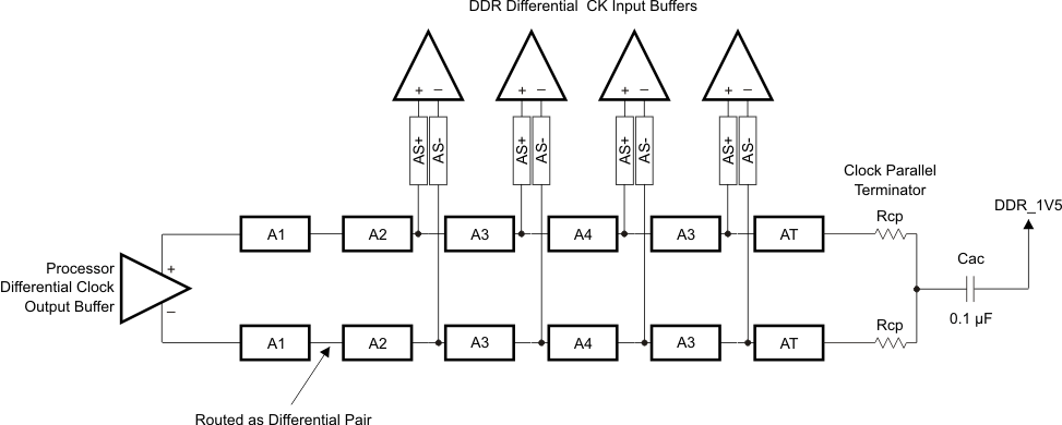 Figure 9-17 CK Topology for Four x8 DDR3 Devices
 Figure 9-18 ADDR_CTRL Topology for Four x8 DDR3 Devices
9.3.2.14.1.2 CK and ADDR_CTRL Routing, Four DDR3 Devices
Figure 9-19 shows the CK routing for four DDR3 devices placed on the same side of the PCB. Figure 9-20 shows the corresponding ADDR_CTRL routing.
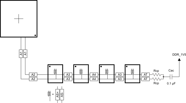 Figure 9-19 CK Routing for Four Single-Side DDR3 Devices
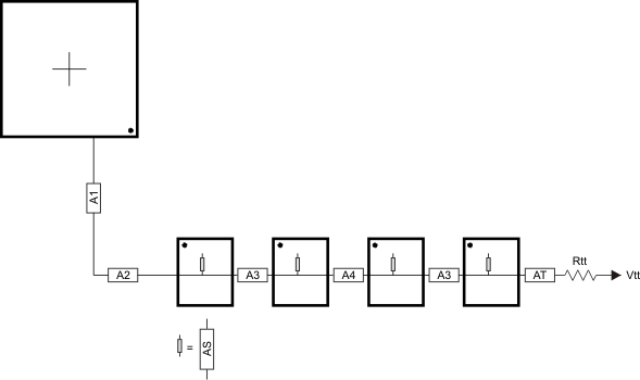 Figure 9-20 ADDR_CTRL Routing for Four Single-Side DDR3 Devices
To save PCB space, the four DDR3 memories may be mounted as two mirrored pairs at a cost of increased routing and assembly complexity. Figure 9-21 and Figure 9-22 show the routing for CK and ADDR_CTRL, respectively, for four DDR3 devices mirrored in a two-pair configuration.
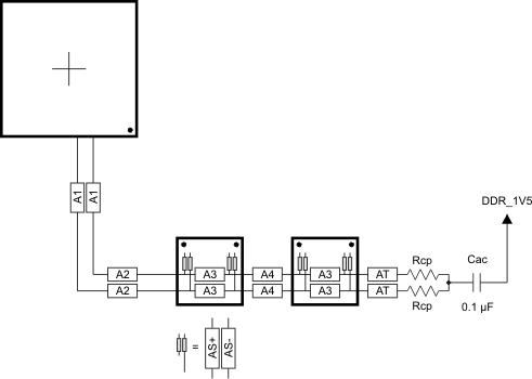 Figure 9-21 CK Routing for Four Mirrored DDR3 Devices
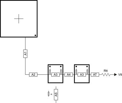 Figure 9-22 ADDR_CTRL Routing for Four Mirrored DDR3 Devices
9.3.2.14.2 Two DDR3 Devices
Two DDR3 devices are supported on the DDR EMIF consisting of two x8 DDR3 devices arranged as one bank (CS), 16 bits wide, or two x16 DDR3 devices arranged as one bank (CS), 32 bits wide. These two devices may be mounted on a single side of the PCB, or may be mirrored in a pair to save board space at a cost of increased routing complexity and parts on the backside of the PCB.
9.3.2.14.2.1 CK and ADDR_CTRL Topologies, Two DDR3 Devices
Figure 9-23 shows the topology of the CK net classes and Figure 9-24 shows the topology for the corresponding ADDR_CTRL net classes.
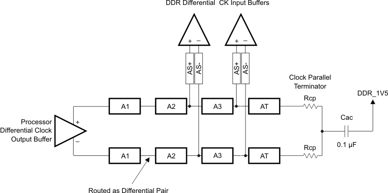 Figure 9-23 CK Topology for Two DDR3 Devices
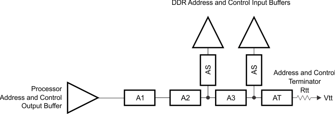 Figure 9-24 ADDR_CTRL Topology for Two DDR3 Devices
9.3.2.14.2.2 CK and ADDR_CTRL Routing, Two DDR3 Devices
Figure 9-25 shows the CK routing for two DDR3 devices placed on the same side of the PCB. Figure 9-26 shows the corresponding ADDR_CTRL routing.
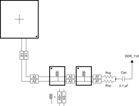 Figure 9-25 CK Routing for Two Single-Side DDR3 Devices
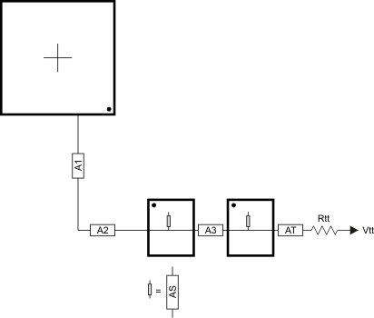 Figure 9-26 ADDR_CTRL Routing for Two Single-Side DDR3 Devices
To save PCB space, the two DDR3 memories may be mounted as a mirrored pair at a cost of increased routing and assembly complexity. Figure 9-27 and Figure 9-28 show the routing for CK and ADDR_CTRL, respectively, for two DDR3 devices mirrored in a single-pair configuration.
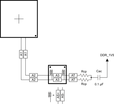 Figure 9-27 CK Routing for Two Mirrored DDR3 Devices
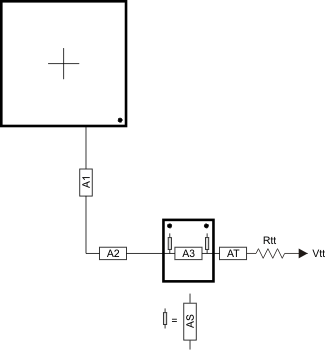 Figure 9-28 ADDR_CTRL Routing for Two Mirrored DDR3 Devices
9.3.2.14.3 One DDR3 Device
A single DDR3 device is supported on the DDR EMIF consisting of one x16 DDR3 device arranged as one bank (CS), 16 bits wide.
9.3.2.14.3.1 CK and ADDR_CTRL Topologies, One DDR3 Device
Figure 9-29 shows the topology of the CK net classes and Figure 9-30 shows the topology for the corresponding ADDR_CTRL net classes.
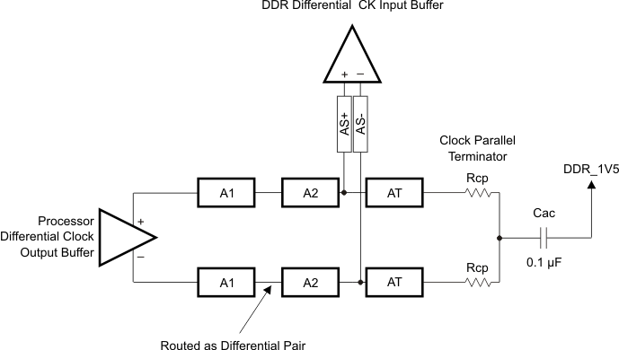 Figure 9-29 CK Topology for One DDR3 Device
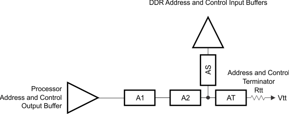 Figure 9-30 ADDR_CTRL Topology for One DDR3 Device
9.3.2.14.3.2 CK and ADDR_CTRL Routing, One DDR3 Device
Figure 9-31 shows the CK routing for one DDR3 device placed on the same side of the PCB. Figure 9-32 shows the corresponding ADDR_CTRL routing.
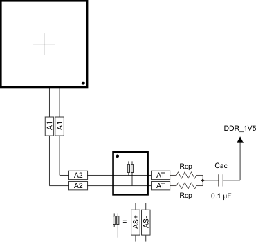 Figure 9-31 CK Routing for One DDR3 Device
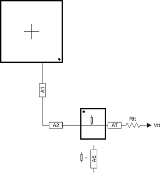 Figure 9-32 ADDR_CTRL Routing for One DDR3 Device
9.3.2.15 Data Topologies and Routing Definition
No matter the number of DDR3 devices used, the data line topology is always point to point, so its definition is simple.
9.3.2.15.1 DQS, DQ and DM Topologies, Any Number of Allowed DDR3 Devices
DQS lines are point-to-point differential, and DQ and DM lines are point-to-point singled ended. Figure 9-33 and Figure 9-34 show these topologies.
 Figure 9-33 DQS Topology
 Figure 9-34 DQ/DM Topology
9.3.2.15.2 DQS, DQ and DM Routing, Any Number of Allowed DDR3 Devices
Figure 9-35 and Figure 9-36 show the DQS, DQ and DM routing.
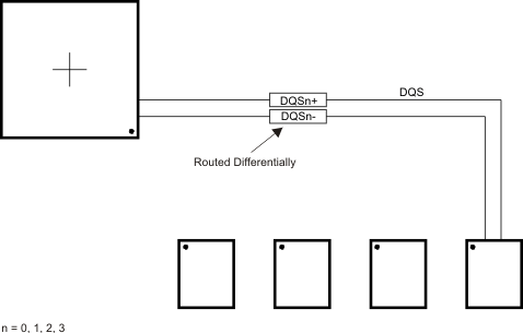 Figure 9-35 DQS Routing With Any Number of Allowed DDR3 Devices
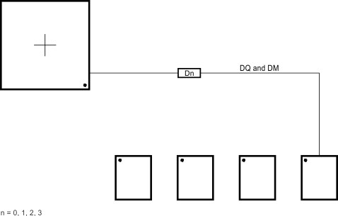 Figure 9-36 DQ and DM Routing With Any Number of Allowed DDR3 Devices
9.3.2.16 Routing Specification
9.3.2.16.1 CK and ADDR_CTRL Routing Specification
Skew within the CK and ADDR_CTRL net classes directly reduces setup and hold margin and, thus, this skew must be controlled. The only way to practically match lengths on a PCB is to lengthen the shorter traces up to the length of the longest net in the net class and its associated clock. A metric to establish this maximum length is Manhattan distance. The Manhattan distance between two points on a PCB is the length between the points when connecting them only with horizontal or vertical segments. A reasonable trace route length is to within a percentage of its Manhattan distance. CACLM is defined as Clock Address Control Longest Manhattan distance.
Given the clock and address pin locations on the processor and the DDR3 memories, the maximum possible Manhattan distance can be determined given the placement. Figure 9-37 and Figure 9-38 show this distance for four loads and two loads, respectively. It is from this distance that the specifications on the lengths of the transmission lines for the address bus are determined. CACLM is determined similarly for other address bus configurations; that is, it is based on the longest net of the CK and ADDR_CTRL net class. For CK and ADDR_CTRL routing, these specifications are contained in Table 9-24.
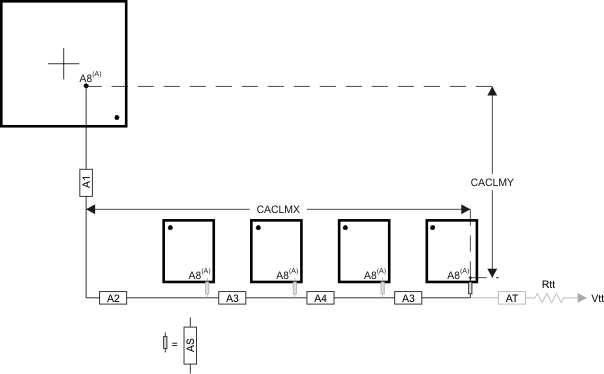
The length of shorter CK and ADDR_CTRL stubs as well as the length of the terminator stub are not included in this length caculation. Non-included lengths are grayed out in the figure.
Assuming A8 is the longest, CALM = CACLMY + CACLMX + 300 mils.
The extra 300 mils allows for routing down lower than the DDR3 memories and returning up to reach A8.
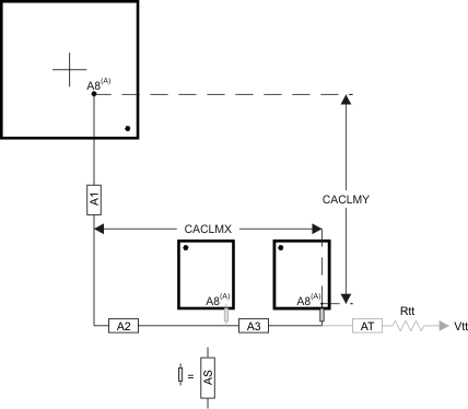
Table 9-24 CK and ADDR_CTRL Routing Specification(1)(2)
| NO. | PARAMETER | MIN | TYP | MAX | UNIT |
|---|---|---|---|---|---|
| 1 | A1+A2 length | 2500 | mils | ||
| 2 | A1+A2 skew | 25 | mils | ||
| 3 | A3 length | 660 | mils | ||
| 4 | A3 skew(3) | 25 | mils | ||
| 5 | A3 skew(4) | 125 | mils | ||
| 6 | A4 length | 660 | mils | ||
| 7 | A4 skew | 25 | mils | ||
| 8 | AS length | 100 | mils | ||
| 9 | AS skew | 100 | mils | ||
| 10 | AS+ and AS- length | 70 | mils | ||
| 11 | AS+ and AS- skew | 5 | mils | ||
| 12 | AT length(5) | 500 | mils | ||
| 13 | AT skew(6) | 100 | mils | ||
| 14 | AT skew(7) | 5 | mils | ||
| 15 | CK and ADDR_CTRL nominal trace length(8) | CACLM-50 | CACLM | CACLM+50 | mils |
| 16 | Center-to-center CK to other DDR3 trace spacing(9) | 4w | |||
| 17 | Center-to-center ADDR_CTRL to other DDR3 trace spacing(9)(10) | 4w | |||
| 18 | Center-to-center ADDR_CTRL to other ADDR_CTRL trace spacing(9) | 3w | |||
| 19 | CK center-to-center spacing(11) | ||||
| 20 | CK spacing to other net(9) | 4w | |||
| 21 | Rcp(12) | Zo-1 | Zo | Zo+ | Ω |
| 22 | Rtt(12)(13) | Zo-5 | Zo | Zo+5 | Ω |
9.3.2.16.2 DQS and DQ Routing Specification
Skew within the DQS, DQ and DM net classes directly reduces setup and hold margin and thus this skew must be controlled. The only way to practically match lengths on a PCB is to lengthen the shorter traces up to the length of the longest net in the net class and its associated clock. As with CK and ADDR_CTRL, a reasonable trace route length is to within a percentage of its Manhattan distance. DQLMn is defined as DQ Longest Manhattan distance n, where n is the byte number. For a 32-bit interface, there are four DQLMs, DQLM0-DQLM3. Likewise, for a 16-bit interface, there are two DQLMs, DQLM0-DQLM1.
NOTE
It is not required, nor is it recommended, to match the lengths across all bytes. Length matching is only required within each byte.
Given the DQS, DQ and DM pin locations on the processor and the DDR3 memories, the maximum possible Manhattan distance can be determined given the placement. Figure 9-39 shows this distance for four loads. It is from this distance that the specifications on the lengths of the transmission lines for the data bus are determined. For DQS, DQ and DM routing, these specifications are contained in Table 9-25.
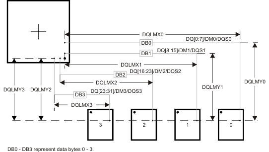
DQLM0 = DQLMX0 + DQLMY0
DQLM1 = DQLMX1 + DQLMY1
DQLM2 = DQLMX2 + DQLMY2
DQLM3 = DQLMX3 + DQLMY3
Table 9-25 Data Routing Specification(1)
| NO. | PARAMETER | MIN | TYP | MAX | UNIT |
|---|---|---|---|---|---|
| 1 | DB0 nominal length(2)(3) | DQLM0 | mils | ||
| 2 | DB1 nominal length(2)(4) | DQLM1 | mils | ||
| 3 | DB2 nominal length(2)(5) | DQLM2 | mils | ||
| 4 | DB3 nominal length(2)(6) | DQLM3 | mils | ||
| 5 | DBn skew(7) | 25 | mils | ||
| 6 | DQSn+ to DQSn- skew | 5 | mils | ||
| 7 | DQSn to DBn skew(7)(8) | 25 | mils | ||
| 8 | Center-to-center DBn to other DDR3 trace spacing(9)(10) | 4w | |||
| 9 | Center-to-center DBn to other DBn trace spacing(9)(11) | 3w | |||
| 10 | DQSn center-to-center spacing(12) | ||||
| 11 | DQSn center-to-center spacing to other net(9) | 4w |
9.3.3 DDR2 and DDR3 Memory Controller Register Descriptions
Table 9-26 DDR2 and DDR3 Memory Controller Registers
| DDR0 HEX ADDRESS | DDR1 HEX ADDRESS | ACRONYM | REGISTER NAME |
|---|---|---|---|
| 0x4C00 0004 | 0x4D00 0004 | SDRSTAT | SDRAM Status |
| 0x4C00 0008 | 0x4D00 0008 | SDRCR | SDRAM Config |
| 0x4C00 000C | 0x4D00 000C | SDRCR2 | SDRAM Config 2 |
| 0x4C00 0010 | 0x4D00 0010 | SDRRCR | SDRAM Refresh Control |
| 0x4C00 0014 | 0x4D00 0014 | SDRRCSR | SDRAM Refresh Control Shadow |
| 0x4C00 0018 | 0x4D00 0018 | SDRTIM1 | SDRAM Timing 1 |
| 0x4C00 001C | 0x4D00 001C | SDRTIM1SR | SDRAM Timing 1 Shadow |
| 0x4C00 0020 | 0x4D00 0020 | SDRTIM2 | SDRAM Timing 2 |
| 0x4C00 0024 | 0x4D00 0024 | SDRTIM2SR | SDRAM Timing 2 Shadow |
| 0x4C00 0028 | 0x4D00 0028 | SDRTIM3 | SDRAM Timing 3 |
| 0x4C00 002C | 0x4D00 002C | SDRTIM3SR | SDRAM Timing 3 Shadow |
| 0x4C00 0038 | 0x4D00 0038 | PMCR | Power Management Control |
| 0x4C00 003C | 0x4D00 003C | PMCSR | Power Management Control Shadow |
| 0x4C00 0054 | 0x4D00 0054 | PBBPR | Peripheral Bus Burst Priority |
| 0x4C00 00A0 | 0x4D00 00A0 | EOI | End of Interrupt |
| 0x4C00 00A4 | 0x4D00 00A4 | SOIRSR | System OCP Interrupt Raw Status |
| 0x4C00 00AC | 0x4D00 00AC | SOISR | System OCP Interrupt Status |
| 0x4C00 00B4 | 0x4D00 00B4 | SOIESR | System OCP Interrupt Enable Set |
| 0x4C00 00BC | 0x4D00 00BC | SOIECR | System OCP Interrupt Enable Clear |
| 0x4C00 00C8 | 0x4D00 00C8 | ZQCR | SDRAM output Impedance Calibration Config |
| 0x4C00 00DC | 0x4D00 00DC | RWLCR | Read-Write Leveling Control |
| 0x4C00 00E4 | 0x4D00 00E4 | DDRPHYCR | DDR PHY Control |
| 0x4C00 00E8 | 0x4D00 00E8 | DDRPHYCSR | DDR PHY Control Shadow |
9.3.4 DDR2 and DDR3 PHY Register Descriptions
Table 9-27 DDR2 and DDR3 PHY Registers
| DDR0 HEX ADDRESS | DDR1 HEX ADDRESS | ACRONYM | REGISTER NAME |
|---|---|---|---|
| 0x4819 800C | 0x4819 A00C | CMD0_IO_CONFIG_I_0 | Command 0 Address and Command Pad Configuration |
| 0x4819 8010 | 0x4819 A010 | CMD0_IO_CONFIG_I_CLK_0 | Command 0 Clock Pad Configuration |
| 0x4819 8014 | 0x4819 A014 | CMD0_IO_CONFIG_SR_0 | Command 0 Address and Command Slew Rate Configuration |
| 0x4819 8018 | 0x4819 A018 | CMD0_IO_CONFIG_SR_CLK_0 | Command 0 Clock Pad Slew Rate Configuration |
| 0x4819 801C | 0x4819 A01C | CMD0_REG_PHY_CTRL_SLAVE_RATIO_0 | Command 0 Address and Command Slave Ratio |
| 0x4819 802C | 0x4819 A02C | CMD0_REG_PHY_INVERT_CLKOUT_0 | Command 0 Invert Clockout Selection |
| 0x4819 8040 | 0x4819 A040 | CMD1_IO_CONFIG_I_0 | Command 1 Address and Command Pad Configuration |
| 0x4819 8044 | 0x4819 A044 | CMD1_IO_CONFIG_I_CLK_0 | Command 1 Clock Pad Configuration |
| 0x4819 8048 | 0x4819 A048 | CMD1_IO_CONFIG_SR_0 | Command 1 Address and Command Slew Rate Configuration |
| 0x4819 804C | 0x4819 A04C | CMD1_IO_CONFIG_SR_CLK_0 | Command 1 Clock Pad Slew Rate Configuration |
| 0x4819 8050 | 0x4819 A050 | CMD1_REG_PHY_CTRL_SLAVE_RATIO_0 | Command 1 Address and Command Slave Ratio |
| 0x4819 8060 | 0x4819 A060 | CMD1_REG_PHY_INVERT_CLKOUT_0 | Command 1 Invert Clockout Selection |
| 0x4819 8074 | 0x4819 A074 | CMD2_IO_CONFIG_I_0 | Command 2 Address and Command Pad Configuration |
| 0x4819 8078 | 0x4819 A078 | CMD2_IO_CONFIG_I_CLK_0 | Command 2 Clock Pad Configuration |
| 0x4819 807C | 0x4819 A07C | CMD2_IO_CONFIG_SR_0 | Command 2 Address and Command Slew Rate Configuration |
| 0x4819 8080 | 0x4819 A080 | CMD2_IO_CONFIG_SR_CLK_0 | Command 2 Clock Pad Slew Rate Configuration |
| 0x4819 8084 | 0x4819 A084 | CMD2_REG_PHY_CTRL_SLAVE_RATIO_0 | Command 2 Address and Command Slave Ratio |
| 0x4819 8094 | 0x4819 A094 | CMD2_REG_PHY_INVERT_CLKOUT_0 | Command 2 Invert Clockout Selection |
| 0x4819 80A8 | 0x4819 A0A8 | DATA0_IO_CONFIG_I_0 | Data Macro 0 Data Pad Configuration |
| 0x4819 80AC | 0x4819 A0AC | DATA0_IO_CONFIG_I_CLK_0 | Data Macro 0 Data Strobe Pad Configuration |
| 0x4819 80B0 | 0x4819 A0B0 | DATA0_IO_CONFIG_SR_0 | Data Macro 0 Data Slew Rate Configuration |
| 0x4819 80B4 | 0x4819 A0B4 | DATA0_IO_CONFIG_SR_CLK_0 | Data Macro 0 Data Strobe Slew Rate Configuration |
| 0x4819 80C8 | 0x4819 A0C8 | DATA0_REG_PHY_RD_DQS_SLAVE_RATIO_0 | Data Macro 0 Read DQS Slave Ratio |
| 0x4819 80DC | 0x4819 A0DC | DATA0_REG_PHY_WR_DQS_SLAVE_RATIO_0 | Data Macro 0 Write DQS Slave Ratio |
| 0x4819 80F0 | 0x4819 A0F0 | DATA0_REG_PHY_WRLVL_INIT_RATIO_0 | Data Macro 0 Write Leveling Init Ratio |
| 0x4819 80F8 | 0x4819 A0F8 | DATA0_REG_PHY_WRLVL_INIT_MODE_0 | Data Macro 0 Write Leveling Init Mode Ratio Selection |
| 0x4819 80FC | 0x4819 A0FC | DATA0_REG_PHY_GATELVL_INIT_RATIO_0 | Data Macro 0 DQS Gate Training Init Ratio |
| 0x4819 8104 | 0x4819 A104 | DATA0_REG_PHY_GATELVL_INIT_MODE_0 | Data Macro 0 DQS Gate Training Init Mode Ratio Selection |
| 0x4819 8108 | 0x4819 A108 | DATA0_REG_PHY_FIFO_WE_SLAVE_RATIO_0 | Data Macro 0 DQS Gate Slave Ratio |
| 0x4819 8120 | 0x4819 A120 | DATA0_REG_PHY_WR_DATA_SLAVE_RATIO_0 | Data Macro 0 Write Data Slave Ratio |
| 0x4819 8134 | 0x4819 A134 | DATA0_REG_PHY_USE_RANK0_DELAYS | Data Macro 0 Delay Selection |
| 0x4819 814C | 0x4819 A14C | DATA1_IO_CONFIG_I_0 | Data Macro 1 Data Pad Configuration |
| 0x4819 8150 | 0x4819 A150 | DATA1_IO_CONFIG_I_CLK_0 | Data Macro 1 Data Strobe Pad Configuration |
| 0x4819 8154 | 0x4819 A154 | DATA1_IO_CONFIG_SR_0 | Data Macro 1 Data Slew Rate Configuration |
| 0x4819 8158 | 0x4819 A158 | DATA1_IO_CONFIG_SR_CLK_0 | Data Macro 1 Data Strobe Slew Rate Configuration |
| 0x4819 816C | 0x4819 A16C | DATA1_REG_PHY_RD_DQS_SLAVE_RATIO_0 | Data Macro 1 Read DQS Slave Ratio |
| 0x4819 8180 | 0x4819 A180 | DATA1_REG_PHY_WR_DQS_SLAVE_RATIO_0 | Data Macro 1 Write DQS Slave Ratio |
| 0x4819 8194 | 0x4819 A194 | DATA1_REG_PHY_WRLVL_INIT_RATIO_0 | Data Macro 1 Write Leveling Init Ratio |
| 0x4819 819C | 0x4819 A19C | DATA1_REG_PHY_WRLVL_INIT_MODE_0 | Data Macro 1 Write Leveling Init Mode Ratio Selection |
| 0x4819 81A0 | 0x4819 A1A0 | DATA1_REG_PHY_GATELVL_INIT_RATIO_0 | Data Macro 1 DQS Gate Training Init Ratio |
| 0x4819 81A8 | 0x4819 A1A8 | DATA1_REG_PHY_GATELVL_INIT_MODE_0 | Data Macro 1 DQS Gate Training Init Mode Ratio Selection |
| 0x4819 81AC | 0x4819 A1AC | DATA1_REG_PHY_FIFO_WE_SLAVE_RATIO_0 | Data Macro 1 DQS Gate Slave Ratio |
| 0x4819 81C4 | 0x4819 A1C4 | DATA1_REG_PHY_WR_DATA_SLAVE_RATIO_0 | Data Macro 1 Write Data Slave Ratio |
| 0x4819 81D8 | 0x4819 A1D8 | DATA1_REG_PHY_USE_RANK0_DELAYS | Data Macro 1 Delay Selection |
| 0x4819 81F0 | 0x4819 A1F0 | DATA2_IO_CONFIG_I_0 | Data Macro 2 Data Pad Configuration |
| 0x4819 81F4 | 0x4819 A1F4 | DATA2_IO_CONFIG_I_CLK_0 | Data Macro 2 Data Strobe Pad Configuration |
| 0x4819 81F8 | 0x4819 A1F8 | DATA2_IO_CONFIG_SR_0 | Data Macro 2 Data Slew Rate Configuration |
| 0x4819 81FC | 0x4819 A1FC | DATA2_IO_CONFIG_SR_CLK_0 | Data Macro 2 Data Strobe Slew Rate Configuration |
| 0x4819 8210 | 0x4819 A210 | DATA2_REG_PHY_RD_DQS_SLAVE_RATIO_0 | Data Macro 2 Read DQS Slave Ratio |
| 0x4819 8224 | 0x4819 A224 | DATA2_REG_PHY_WR_DQS_SLAVE_RATIO_0 | Data Macro 2 Write DQS Slave Ratio |
| 0x4819 8238 | 0x4819 A238 | DATA2_REG_PHY_WRLVL_INIT_RATIO_0 | Data Macro 2 Write Leveling Init Ratio |
| 0x4819 8240 | 0x4819 A240 | DATA2_REG_PHY_WRLVL_INIT_MODE_0 | Data Macro 2 Write Leveling Init Mode Ratio Selection |
| 0x4819 8244 | 0x4819 A244 | DATA2_REG_PHY_GATELVL_INIT_RATIO_0 | Data Macro 2 DQS Gate Training Init Ratio |
| 0x4819 824C | 0x4819 A24C | DATA2_REG_PHY_GATELVL_INIT_MODE_0 | Data Macro 2 DQS Gate Training Init Mode Ratio Selection |
| 0x4819 8250 | 0x4819 A250 | DATA2_REG_PHY_FIFO_WE_SLAVE_RATIO_0 | Data Macro 2 DQS Gate Slave Ratio |
| 0x4819 8268 | 0x4819 A268 | DATA2_REG_PHY_WR_DATA_SLAVE_RATIO_0 | Data Macro 2 Write Data Slave Ratio |
| 0x4819 827C | 0x4819 A27C | DATA2_REG_PHY_USE_RANK0_DELAYS | Data Macro 2 Delay Selection |
| 0x4819 8294 | 0x4819 A294 | DATA3_IO_CONFIG_I_0 | Data Macro 3 Data Pad Configuration |
| 0x4819 8298 | 0x4819 A298 | DATA3_IO_CONFIG_I_CLK_0 | Data Macro 3 Data Strobe Pad Configuration |
| 0x4819 829C | 0x4819 A29C | DATA3_IO_CONFIG_SR_0 | Data Macro 3 Data Slew Rate Configuration |
| 0x4819 82A0 | 0x4819 A2A0 | DATA3_IO_CONFIG_SR_CLK_0 | Data Macro 3 Data Strobe Slew Rate Configuration |
| 0x4819 82B4 | 0x4819 A2B4 | DATA3_REG_PHY_RD_DQS_SLAVE_RATIO_0 | Data Macro 3 Read DQS Slave Ratio |
| 0x4819 82C8 | 0x4819 A2C8 | DATA3_REG_PHY_WR_DQS_SLAVE_RATIO_0 | Data Macro 3 Write DQS Slave Ratio |
| 0x4819 82DC | 0x4819 A2DC | DATA3_REG_PHY_WRLVL_INIT_RATIO_0 | Data Macro 3 Write Leveling Init Ratio |
| 0x4819 82E4 | 0x4819 A2E4 | DATA3_REG_PHY_WRLVL_INIT_MODE_0 | Data Macro 3 Write Leveling Init Mode Ratio Selection |
| 0x4819 82E8 | 0x4819 A2E8 | DATA3_REG_PHY_GATELVL_INIT_RATIO_0 | Data Macro 3 DQS Gate Training Init Ratio |
| 0x4819 82F0 | 0x4819 A2F0 | DATA3_REG_PHY_GATELVL_INIT_MODE_0 | Data Macro 3 DQS Gate Training Init Mode Ratio Selection |
| 0x4819 82F4 | 0x4819 A2F4 | DATA3_REG_PHY_FIFO_WE_SLAVE_RATIO_0 | Data Macro 3 DQS Gate Slave Ratio |
| 0x4819 830C | 0x4819 A30C | DATA3_REG_PHY_WR_DATA_SLAVE_RATIO_0 | Data Macro 3 Write Data Slave Ratio |
| 0x4819 8320 | 0x4819 A320 | DATA3_REG_PHY_USE_RANK0_DELAYS | Data Macro 3 Delay Selection |
| 0x4819 8358 | 0x4819 A358 | DDR_VTP_CTRL_0 | DDR VTP Control |
9.3.5 DDR2 and DDR3 Memory Controller Electrical Data and Timing
Section 9.3.1, DDR2 Routing Specifications and Section 9.3.2, DDR3 Routing Specifications specify a complete DDR2 and DDR3 interface solution for the device. TI has performed the simulation and system characterization to ensure all DDR2 and DDR3 interface timings in this solution are met.
TI only supports board designs that follow the specifications outlined in the DDR2 Routing Specifications and DDR3 Routing Specifications sections of this data sheet.
9.4 Emulation Features and Capability
9.4.1 Advanced Event Triggering (AET)
The device supports Advanced Event Triggering (AET). This capability can be used to debug complex problems as well as understand performance characteristics of user applications. AET provides the following capabilities:
- Hardware Program Breakpoints: specify addresses or address ranges that can generate events such as halting the processor or triggering the trace capture.
- Data Watchpoints: specify data variable addresses, address ranges, or data values that can generate events such as halting the processor or triggering the trace capture.
- Counters: count the occurrence of an event or cycles for performance monitoring.
- State Sequencing: allows combinations of hardware program breakpoints and data watchpoints to precisely generate events for complex sequences.
For more information on AET, see the following documents:
9.4.2 Trace
The device supports Trace at the Cortex™-A8, C674x, and System levels. Trace is a debug technology that provides a detailed, historical account of application code execution, timing, and data accesses. Trace collects, compresses, and exports debug information for analysis. The debug information can be exported to the Embedded Trace Buffer (ETB), or to the 5-pin Trace Interface (system trace only). Trace works in real-time and does not impact the execution of the system.
For more information on board design guidelines for Trace Advanced Emulation, see the Emulation and Trace Headers Technical Reference Manual (literature number SPRU655).
9.4.3 IEEE 1149.1 JTAG
The JTAG (IEEE Standard 1149.1-1990 Standard-Test-Access Port and Boundary Scan Architecture) interface is used for BSDL testing and emulation of the device. The TRST pin only needs to be released when it is necessary to use a JTAG controller to debug the device or exercise the device's boundary scan functionality. For maximum reliability, the device includes an internal pulldown (IPD) on the TRST pin to ensure that TRST is always asserted upon power up and the device's internal emulation logic is always properly initialized. JTAG controllers from Texas Instruments actively drive TRST high. However, some third-party JTAG controllers may not drive TRST high but expect the use of a pullup resistor on TRST. When using this type of JTAG controller, assert TRST to initialize the device after powerup and externally drive TRST high before attempting any emulation or boundary-scan operations.
The main JTAG features include:
- 32KB embedded trace buffer (ETB)
- 5-pin system trace interface for debug
- Supports Advanced Event Triggering (AET)
- All processors can be emulated via JTAG ports
- All functions on EMU pins of the device:
- EMU[1:0] - cross-triggering, boot mode (WIR), STM trace
- EMU[4:2] - STM trace only (single direction)
- EMU[2] - only valid pin to use as clock
9.4.3.1 JTAG ID (JTAGID) Register Description
Table 9-28 JTAG ID Register(1)
| HEX ADDRESS | ACRONYM | REGISTER NAME |
|---|---|---|
| 0x4814 0600 | JTAGID | JTAG Identification Register(2) |
The JTAG ID register is a read-only register that identifies to the customer the JTAG device ID. For this device, the JTAG ID register resides at address location 0x4814 0600. The register hex value for the device depends on the silicon revision being used. For more information, see the TMS320DM816x DaVinci Digital Media ProcessorsSilicon Errata (literature number SPRZ329). For the actual register bit names and their associated bit field descriptions, see Figure 9-40 and Table 9-29.
| 31 | 28 | 27 | 12 | 11 | 1 | 0 | |||||||||||||||||||||||||
| VARIANT (4-bit) | PART NUMBER (16-bit) | MANUFACTURER (11-bit) | LSB | ||||||||||||||||||||||||||||
| R-x | R-1011 1000 0001 1110 | R-0000 0010 111 | R-1 | ||||||||||||||||||||||||||||
| LEGEND: R/W = Read/Write; R = Read only; -n = value after reset |
Table 9-29 JTAG ID Register Selection Bit Descriptions
| Bit | Field | Description |
|---|---|---|
| 31:28 | VARIANT | Variant (4-bit) value. Device value: The value of this field depends on the silicon revision being used. For more information, see the TMS320DM816x DaVinci Digital Media ProcessorsSilicon Errata (literature number SPRZ329). |
| 27:12 | PART NUMBER | Part Number (16-bit) value. Device value: 0xB81E |
| 11:1 | MANUFACTURER | Manufacturer (11-bit) value. Device value: 0x017 |
| 0 | LSB | LSB. This bit is read as a 1 for this device. |
9.4.3.2 JTAG Electrical Data and Timing
Table 9-30 Timing Requirements for IEEE 1149.1 JTAG
(see Figure 9-41)| NO. | MIN | MAX | UNIT | ||
|---|---|---|---|---|---|
| 1 | tc(TCK) | Cycle time, TCK | 51.15 | ns | |
| 1a | tw(TCKH) | Pulse duration, TCK high (40% of tc) | 20.46 | ns | |
| 1b | tw(TCKL) | Pulse duration, TCK low (40% of tc) | 20.46 | ns | |
| 3 | tsu(TDI-TCK) | Input setup time, TDI valid to TCK high (20% of (tc * 0.5)) | 5.115 | ns | |
| 3 | tsu(TMS-TCK) | Input setup time, TMS valid to TCK high (20% of (tc * 0.5)) | 5.115 | ns | |
| 4 | th(TCK-TDI) | Input hold time, TDI valid from TCK high | 10 | ns | |
| th(TCK-TMS) | Input hold time, TMS valid from TCK high | 10 | ns | ||
Table 9-31 Switching Characteristics Over Recommended Operating Conditions for IEEE 1149.1 JTAG
(see Figure 9-41)| NO. | PARAMETER | MIN | MAX | UNIT | |
|---|---|---|---|---|---|
| 2 | td(TCKL-TDOV) | Delay time, TCK low to TDO valid | 0 | 23.575(1) | ns |
 Figure 9-41 JTAG Timing
Table 9-32 Timing Requirements for IEEE 1149.1 JTAG With RTCK
(see Figure 9-41)| NO. | MIN | MAX | UNIT | ||
|---|---|---|---|---|---|
| 1 | tc(TCK) | Cycle time, TCK | 51.15 | ns | |
| 1a | tw(TCKH) | Pulse duration, TCK high (40% of tc) | 20.46 | ns | |
| 1b | tw(TCKL) | Pulse duration, TCK low (40% of tc) | 20.46 | ns | |
| 3 | tsu(TDI-TCK) | Input setup time, TDI valid to TCK high (20% of (tc * 0.5)) | 5.115 | ns | |
| 3 | tsu(TMS-TCK) | Input setup time, TMS valid to TCK high (20% of (tc * 0.5)) | 5.115 | ns | |
| 4 | th(TCK-TDI) | Input hold time, TDI valid from TCK high | 10 | ns | |
| th(TCK-TMS) | Input hold time, TMS valid from TCK high | 10 | ns | ||
Table 9-33 Switching Characteristics Over Recommended Operating Conditions for IEEE 1149.1 JTAG With RTCK
(see Figure 9-42)| NO. | PARAMETER | MIN | MAX | UNIT | |
|---|---|---|---|---|---|
| 5 | td(TCK-RTCK) | Delay time, TCK to RTCK with no selected subpaths (that is, ICEPick module is the only tap selected - when the ARM is in the scan chain, the delay time is a function of the ARM functional clock.) | 0 | 21 | ns |
| 6 | tc(RTCK) | Cycle time, RTCK | 51.15 | ns | |
| 7 | tw(RTCKH) | Pulse duration, RTCK high (40% of tc) | 20.46 | ns | |
| 8 | tw(RTCKL) | Pulse duration, RTCK low (40% of tc) | 20.46 | ns | |
 Figure 9-42 JTAG With RTCK Timing
9.4.4 IEEE 1149.7 cJTAG
Besides the standard (legacy) JTAG mode of operation, the target debug interface can also be switched to a compressed JTAG (cJTAG) mode of operation, commonly referred to as IEEE1149.7 standard. An IEEE1149.7 adapter module runs a 2-pin communication protocol on top of an IEEE1149.1 JTAG TAP. The debug-IP logic serializes the IEEE1149.1 transactions, using a variety of compression formats, to reduce the number of pins needed to implement a JTAG debug port. This device implements only a subset of the IEEE1149.7 protocol; it supports Class 0 and Class 1 operation. On this device the cJTAG ID[7:0] is tied to 0x00.
NOTE
The default setting of the scan port is IEEE 1149.1. A cJTAG emulator connected only to TCLK and TMS can re-configure the port to cJTAG by scanning in a special command sequence. For the scan sequence required to switch modes, see the IEEE1149.7 specification.
9.5 Enhanced Direct Memory Access (EDMA) Controller
The EDMA controller handles all data transfers between memories and the device slave peripherals on the device. These data transfers include cache servicing, non-cacheable memory accesses, user-programmed data transfers, and host accesses.
9.5.1 EDMA Channel Synchronization Events
The EDMA channel controller supports up to 64 channels that service peripherals and memory. Each EDMA channel is mapped to a default EDMA synchronization event as shown in Table 9-34. By default, each event uses the parameter entry that matches its event number. However, because the device includes a channel mapping feature, each event may be mapped to any of 512 parameter table entries. For more detailed information on the EDMA module and how EDMA events are enabled, captured, processed, linked, chained, and cleared, see the EDMA chapter in the TMS320DM816x DaVinci Digital Media Processors Technical Reference Manual (literature number SPRUGX8).
Table 9-34 EDMA Default Synchronization Events
| EVENT NUMBER | DEFAULT EVENT NAME | DEFAULT EVENT DESCRIPTION |
|---|---|---|
| 0 - 7 | - | Unused |
| 8 | AXEVT0 | McASP0 Transmit |
| 9 | AREVT0 | McASP0 Receive |
| 10 | AXEVT1 | McASP1 Transmit |
| 11 | AREVT1 | McASP1 Receive |
| 12 | AXEVT2 | McASP2 Transmit |
| 13 | AREVT2 | McASP2 Receive |
| 14 | BXEVT | McBSP Transmit |
| 15 | BREVT | McBSP Receive |
| 16 | SPIXEVT0 | SPI0 Transmit 0 |
| 17 | SPIREVT0 | SPI0 Receive 0 |
| 18 | SPIXEVT1 | SPI0 Transmit 1 |
| 19 | SPIREVT1 | SPI0 Receive 1 |
| 20 | SPIXEVT2 | SPI0 Transmit 2 |
| 21 | SPIREVT2 | SPI0 Receive 2 |
| 22 | SPIXEVT3 | SPI0 Transmit 3 |
| 23 | SPIREVT3 | SPI0 Receive 3 |
| 24 | SDTXEVT | SD0 Transmit |
| 25 | SDRXEVT | SD0 Receive |
| 26 | UTXEVT0 | UART0 Transmit |
| 27 | URXEVT0 | UART0 Receive |
| 28 | UTXEVT1 | UART1 Transmit |
| 29 | URXEVT1 | UART1 Receive |
| 30 | UTXEVT2 | UART2 Transmit |
| 31 | URXEVT2 | UART2 Receive |
| 32 - 47 | - | Unused |
| 48 | TINT4 | TIMER4 |
| 49 | TINT5 | TIMER5 |
| 50 | TINT6 | TIMER6 |
| 51 | TINT7 | TIMER7 |
| 52 | GPMCEVT | GPMC |
| 53 | HDMIEVT | HDMI |
| 54 - 57 | - | Unused |
| 58 | I2CTXEVT0 | I2C0 Transmit |
| 59 | I2CRXEVT0 | I2C0 Receive |
| 60 | I2CTXEVT1 | I2C1 Transmit |
| 61 | I2CRXEVT1 | I2C1 Receive |
| 62 - 63 | - | Unused |
9.5.2 EDMA Peripheral Register Descriptions
Table 9-35 EDMA Channel Controller (EDMA TPCC) Control Registers
| HEX ADDRESS | ACRONYM | REGISTER NAME |
|---|---|---|
| 0x4900 0000 | PID | Peripheral Identification |
| 0x4900 0004 | CCCFG | EDMA3CC Configuration |
| 0x4900 0100 - 0x4900 01FC | DCHMAP0-63 | DMA Channel 0-63 Mappings |
| 0x4900 0200 | QCHMAP0 | QDMA Channel 0 Mapping |
| 0x4900 0204 | QCHMAP1 | QDMA Channel 1 Mapping |
| 0x4900 0208 | QCHMAP2 | QDMA Channel 2 Mapping |
| 0x4900 020C | QCHMAP3 | QDMA Channel 3 Mapping |
| 0x4900 0210 | QCHMAP4 | QDMA Channel 4 Mapping |
| 0x4900 0214 | QCHMAP5 | QDMA Channel 5 Mapping |
| 0x4900 0218 | QCHMAP6 | QDMA Channel 6 Mapping |
| 0x4900 021C | QCHMAP7 | QDMA Channel 7 Mapping |
| 0x4900 0240 | DMAQNUM0 | DMA Queue Number 0 |
| 0x4900 0244 | DMAQNUM1 | DMA Queue Number 1 |
| 0x4900 0248 | DMAQNUM2 | DMA Queue Number 2 |
| 0x4900 024C | DMAQNUM3 | DMA Queue Number 3 |
| 0x4900 0250 | DMAQNUM4 | DMA Queue Number 4 |
| 0x4900 0254 | DMAQNUM5 | DMA Queue Number 5 |
| 0x4900 0258 | DMAQNUM6 | DMA Queue Number 6 |
| 0x4900 025C | DMAQNUM7 | DMA Queue Number 7 |
| 0x4900 0260 | QDMAQNUM | QDMA Queue Number |
| 0x4900 0284 | QUEPRI | Queue Priority |
| 0x4900 0300 | EMR | Event Missed |
| 0x4900 0304 | EMRH | Event Missed High |
| 0x4900 0308 | EMCR | Event Missed Clear |
| 0x4900 030C | EMCRH | Event Missed Clear High |
| 0x4900 0310 | QEMR | QDMA Event Missed |
| 0x4900 0314 | QEMCR | QDMA Event Missed Clear |
| 0x4900 0318 | CCERR | EDMA3CC Error |
| 0x4900 031C | CCERRCLR | EDMA3CC Error Clear |
| 0x4900 0320 | EEVAL | Error Evaluate |
| 0x4900 0340 | DRAE0 | DMA Region Access Enable for Region 0 |
| 0x4900 0344 | DRAEH0 | DMA Region Access Enable High for Region 0 |
| 0x4900 0348 | DRAE1 | DMA Region Access Enable for Region 1 |
| 0x4900 034C | DRAEH1 | DMA Region Access Enable High for Region 1 |
| 0x4900 0350 | DRAE2 | DMA Region Access Enable for Region 2 |
| 0x4900 0354 | DRAEH2 | DMA Region Access Enable High for Region 2 |
| 0x4900 0358 | DRAE3 | DMA Region Access Enable for Region 3 |
| 0x4900 035C | DRAEH3 | DMA Region Access Enable High for Region 3 |
| 0x4900 0360 | DRAE4 | DMA Region Access Enable for Region 4 |
| 0x4900 0364 | DRAEH4 | DMA Region Access Enable High for Region 4 |
| 0x4900 0368 | DRAE5 | DMA Region Access Enable for Region 5 |
| 0x4900 036C | DRAEH5 | DMA Region Access Enable High for Region 5 |
| 0x4900 0370 | DRAE6 | DMA Region Access Enable for Region 6 |
| 0x4900 0374 | DRAEH6 | DMA Region Access Enable High for Region 6 |
| 0x4900 0378 | DRAE7 | DMA Region Access Enable for Region 7 |
| 0x4900 037C | DRAEH7 | DMA Region Access Enable High for Region 7 |
| 0x4900 0380 - 0x4900 039C | QRAE0-7 | QDMA Region Access Enable for Region 0-7 |
| 0x4900 0400 - 0x4900 04FC | Q0E0-Q3E15 | Event Queue Entry Q0E0-Q3E15 |
| 0x4900 0600 - 0x4900 060C | QSTAT0-3 | Queue Status 0-3 |
| 0x4900 0620 | QWMTHRA | Queue Watermark Threshold A |
| 0x4900 0640 | CCSTAT | EDMA3CC Status |
| 0x4900 0800 | MPFAR | Memory Protection Fault Address |
| 0x4900 0804 | MPFSR | Memory Protection Fault Status |
| 0x4900 0808 | MPFCR | Memory Protection Fault Command |
| 0x4900 080C | MPPAG | Memory Protection Page Attribute Global |
| 0x4900 0810 - 0x4900 082C | MPPA0-7 | Memory Protection Page Attribute 0-7 |
| 0x4900 1000 | ER | Event |
| 0x4900 1004 | ERH | Event High |
| 0x4900 1008 | ECR | Event Clear |
| 0x4900 100C | ECRH | Event Clear High |
| 0x4900 1010 | ESR | Event Set |
| 0x4900 1014 | ESRH | Event Set High |
| 0x4900 1018 | CER | Chained Event |
| 0x4900 101C | CERH | Chained Event High |
| 0x4900 1020 | EER | Event Enable |
| 0x4900 1024 | EERH | Event Enable High |
| 0x4900 1028 | EECR | Event Enable Clear |
| 0x4900 102C | EECRH | Event Enable Clear High |
| 0x4900 1030 | EESR | Event Enable Set |
| 0x4900 1034 | EESRH | Event Enable Set High |
| 0x4900 1038 | SER | Secondary Event |
| 0x4900 103C | SERH | Secondary Event High |
| 0x4900 1040 | SECR | Secondary Event Clear |
| 0x4900 1044 | SECRH | Secondary Event Clear High |
| 0x4900 1050 | IER | Interrupt Enable |
| 0x4900 1054 | IERH | Interrupt Enable High |
| 0x4900 1058 | IECR | Interrupt Enable Clear |
| 0x4900 105C | IECRH | Interrupt Enable Clear High |
| 0x4900 1060 | IESR | Interrupt Enable Set |
| 0x4900 1064 | IESRH | Interrupt Enable Set High |
| 0x4900 1068 | IPR | Interrupt Pending |
| 0x4900 106C | IPRH | Interrupt Pending High |
| 0x4900 1070 | ICR | Interrupt Clear |
| 0x4900 1074 | ICRH | Interrupt Clear High |
| 0x4900 1078 | IEVAL | Interrupt Evaluate |
| 0x4900 1080 | QER | QDMA Event |
| 0x4900 1084 | QEER | QDMA Event Enable |
| 0x4900 1088 | QEECR | QDMA Event Enable Clear |
| 0x4900 108C | QEESR | QDMA Event Enable Set |
| 0x4900 1090 | QSER | QDMA Secondary Event |
| 0x4900 1094 | QSECR | QDMA Secondary Event Clear |
| Shadow Region 0 Channel Registers | ||
| 0x4900 2000 | ER | Event |
| 0x4900 2004 | ERH | Event High |
| 0x4900 2008 | ECR | Event Clear |
| 0x4900 200C | ECRH | Event Clear High |
| 0x4900 2010 | ESR | Event Set |
| 0x4900 2014 | ESRH | Event Set High |
| 0x4900 2018 | CER | Chained Event |
| 0x4900 201C | CERH | Chained Event High |
| 0x4900 2020 | EER | Event Enable |
| 0x4900 2024 | EERH | Event Enable High |
| 0x4900 2028 | EECR | Event Enable Clear |
| 0x4900 202C | EECRH | Event Enable Clear High |
| 0x4900 2030 | EESR | Event Enable Set |
| 0x4900 2034 | EESRH | Event Enable Set High |
| 0x4900 2038 | SER | Secondary Event |
| 0x4900 203C | SERH | Secondary Event High |
| 0x4900 2040 | SECR | Secondary Event Clear |
| 0x4900 2044 | SECRH | Secondary Event Clear High |
| 0x4900 2050 | IER | Interrupt Enable |
| 0x4900 2054 | IERH | Interrupt Enable High |
| 0x4900 2058 | IECR | Interrupt Enable Clear |
| 0x4900 205C | IECRH | Interrupt Enable Clear High |
| 0x4900 2060 | IESR | Interrupt Enable Set |
| 0x4900 2064 | IESRH | Interrupt Enable Set High |
| 0x4900 2068 | IPR | Interrupt Pending |
| 0x4900 206C | IPRH | Interrupt Pending High |
| 0x4900 2070 | ICR | Interrupt Clear |
| 0x4900 2074 | ICRH | Interrupt Clear High |
| 0x4900 2078 | IEVAL | Interrupt Evaluate |
| 0x4900 2080 | QER | QDMA Event |
| 0x4900 2084 | QEER | QDMA Event Enable |
| 0x4900 2088 | QEECR | QDMA Event Enable Clear |
| 0x4900 208C | QEESR | QDMA Event Enable Set |
| 0x4900 2090 | QSER | QDMA Secondary Event |
| 0x4900 2094 | QSECR | QDMA Secondary Event Clear |
| 0x4900 2200 - 0x4900 2294 | - | Shadow Region 1 Channels |
| 0x4900 2400 - 0x4900 2494 | - | Shadow Region 2 Channels |
| ... | ... | |
| 0x4900 2E00 - 0x4900 2E94 | - | Shadow Channels for MP Space 7 |
Table 9-36 EDMA Transfer Controller (EDMA TPTC) Control Registers
| TPTC0 HEX ADDRESS | TPTC1 HEX ADDRESS | TPTC2 HEX ADDRESS | TPTC3 HEX ADDRESS | ACRONYM | REGISTER NAME |
|---|---|---|---|---|---|
| 0x4980 0000 | 0x4990 0000 | 0x49A0 0000 | 0x49B0 0000 | PID | Peripheral Identification |
| 0x4980 0004 | 0x4990 0004 | 0x49A0 0004 | 0x49B0 0004 | TCCFG | EDMA3TC Configuration |
| 0x4980 0100 | 0x4990 0100 | 0x49A0 0100 | 0x49B0 0100 | TCSTAT | EDMA3TC Channel Status |
| 0x4980 0120 | 0x4990 0120 | 0x49A0 0120 | 0x49B0 0120 | ERRSTAT | Error Status |
| 0x4980 0124 | 0x4990 0124 | 0x49A0 0124 | 0x49B0 0124 | ERREN | Error Enable |
| 0x4980 0128 | 0x4990 0128 | 0x49A0 0128 | 0x49B0 0128 | ERRCLR | Error Clear |
| 0x4980 012C | 0x4990 012C | 0x49A0 012C | 0x49B0 012C | ERRDET | Error Details |
| 0x4980 0130 | 0x4990 0130 | 0x49A0 0130 | 0x49B0 0130 | ERRCMD | Error Interrupt Command |
| 0x4980 0140 | 0x4990 0140 | 0x49A0 0140 | 0x49B0 0140 | RDRATE | Read Rate Register |
| 0x4980 0240 | 0x4990 0240 | 0x49A0 0240 | 0x49B0 0240 | SAOPT | Source Active Options |
| 0x4980 0244 | 0x4990 0244 | 0x49A0 0244 | 0x49B0 0244 | SASRC | Source Active Source Address |
| 0x4980 0248 | 0x4990 0248 | 0x49A0 0248 | 0x49B0 0248 | SACNT | Source Active Count |
| 0x4980 024C | 0x4990 024C | 0x49A0 024C | 0x49B0 024C | SADST | Source Active Destination Address |
| 0x4980 0250 | 0x4990 0250 | 0x49A0 0250 | 0x49B0 0250 | SABIDX | Source Active Source B-Index |
| 0x4980 0254 | 0x4990 0254 | 0x49A0 0254 | 0x49B0 0254 | SAMPPRXY | Source Active Memory Protection Proxy |
| 0x4980 0258 | 0x4990 0258 | 0x49A0 0258 | 0x49B0 0258 | SACNTRLD | Source Active Count Reload |
| 0x4980 025C | 0x4990 025C | 0x49A0 025C | 0x49B0 025C | SASRCBREF | Source Active Source Address B-Reference |
| 0x4980 0260 | 0x4990 0260 | 0x49A0 0260 | 0x49B0 0260 | SADSTBREF | Source Active Destination Address B-Reference |
| 0x4980 0280 | 0x4990 0280 | 0x49A0 0280 | 0x49B0 0280 | DFCNTRLD | Destination FIFO Set Count Reload |
| 0x4980 0284 | 0x4990 0284 | 0x49A0 0284 | 0x49B0 0284 | DFSRCBREF | Destination FIFO Set Destination Address B Reference |
| 0x4980 0288 | 0x4990 0288 | 0x49A0 0288 | 0x49B0 0288 | DFDSTBREF | Destination FIFO Set Destination Address B Reference |
| 0x4980 0300 | 0x4990 0300 | 0x49A0 0300 | 0x49B0 0300 | DFOPT0 | Destination FIFO Options 0 |
| 0x4980 0304 | 0x4990 0304 | 0x49A0 0304 | 0x49B0 0304 | DFSRC0 | Destination FIFO Source Address 0 |
| 0x4980 0308 | 0x4990 0308 | 0x49A0 0308 | 0x49B0 0308 | DFCNT0 | Destination FIFO Count 0 |
| 0x4980 030C | 0x4990 030C | 0x49A0 030C | 0x49B0 030C | DFDST0 | Destination FIFO Destination Address 0 |
| 0x4980 0310 | 0x4990 0310 | 0x49A0 0310 | 0x49B0 0310 | DFBIDX0 | Destination FIFO BIDX 0 |
| 0x4980 0314 | 0x4990 0314 | 0x49A0 0314 | 0x49B0 0314 | DFMPPRXY0 | Destination FIFO Memory Protection Proxy 0 |
| 0x4980 0340 | 0x4990 0340 | 0x49A0 0340 | 0x49B0 0340 | DFOPT1 | Destination FIFO Options 1 |
| 0x4980 0344 | 0x4990 0344 | 0x49A0 0344 | 0x49B0 0344 | DFSRC1 | Destination FIFO Source Address 1 |
| 0x4980 0348 | 0x4990 0348 | 0x49A0 0348 | 0x49B0 0348 | DFCNT1 | Destination FIFO Count 1 |
| 0x4980 034C | 0x4990 034C | 0x49A0 034C | 0x49B0 034C | DFDST1 | Destination FIFO Destination Address 1 |
| 0x4980 0350 | 0x4990 0350 | 0x49A0 0350 | 0x49B0 0350 | DFBIDX1 | Destination FIFO BIDX 1 |
| 0x4980 0354 | 0x4990 0354 | 0x49A0 0354 | 0x49B0 0354 | DFMPPRXY1 | Destination FIFO Memory Protection Proxy 1 |
| 0x4980 0380 | 0x4990 0380 | 0x49A0 0380 | 0x49B0 0380 | DFOPT2 | Destination FIFO Options 2 |
| 0x4980 0384 | 0x4990 0384 | 0x49A0 0384 | 0x49B0 0384 | DFSRC2 | Destination FIFO Source Address 2 |
| 0x4980 0388 | 0x4990 0388 | 0x49A0 0388 | 0x49B0 0388 | DFCNT2 | Destination FIFO Count 2 |
| 0x4980 038C | 0x4990 038C | 0x49A0 038C | 0x49B0 038C | DFDST2 | Destination FIFO Destination Address 2 |
| 0x4980 0390 | 0x4990 0390 | 0x49A0 0390 | 0x49B0 0390 | DFBIDX2 | Destination FIFO BIDX 2 |
| 0x4980 0394 | 0x4990 0394 | 0x49A0 0394 | 0x49B0 0394 | DFMPPRXY2 | Destination FIFO Memory Protection Proxy 2 |
| 0x4980 03C0 | 0x4990 03C0 | 0x49A0 03C0 | 0x49B0 03C0 | DFOPT3 | Destination FIFO Options 3 |
| 0x4980 03C4 | 0x4990 03C4 | 0x49A0 03C4 | 0x49B0 03C4 | DFSRC3 | Destination FIFO Source Address 3 |
| 0x4980 03C8 | 0x4990 03C8 | 0x49A0 03C8 | 0x49B0 03C8 | DFCNT3 | Destination FIFO Count 3 |
| 0x4980 03CC | 0x4990 03CC | 0x49A0 03CC | 0x49B0 03CC | DFDST3 | Destination FIFO Destination Address 3 |
| 0x4980 03D0 | 0x4990 03D0 | 0x49A0 03D0 | 0x49B0 03D0 | DFBIDX3 | Destination FIFO BIDX 3 |
| 0x4980 03D4 | 0x4990 03D4 | 0x49A0 03D4 | 0x49B0 03D4 | DFMPPRXY3 | Destination FIFO Memory Protection Proxy 3 |
9.6 Ethernet Media Access Controller (EMAC)
The device includes two Ethernet Media Access Controller (EMAC) modules which provide an efficient interface between the device and the networked community. The EMAC supports 10Base-T (10 Mbits per second [Mbps]) and 100Base-TX (100 Mbps) in either half- or full-duplex mode, and 1000Base-T (1000 Mbps) in full-duplex mode, with hardware flow control and quality-of-service (QOS) support. The EMAC controls the flow of packet data from the device to an external PHY. A single MDIO interface is pinned out to control the PHY configuration and status monitoring. Multiple external PHYs can be controlled by the MDIO interface.
The EMAC module conforms to the IEEE 802.3-2002 standard, describing the Carrier Sense Multiple Access with Collision Detection (CSMA/CD) Access Method and Physical Layer specifications. The IEEE 802.3 standard has also been adopted by ISO/IEC and re-designated as ISO/IEC 8802-3:2000(E). Deviating from this standard, the EMAC module does not use the transmit coding error signal, MTXER. Instead of driving the error pin when an underflow condition occurs on a transmitted frame, the EMAC intentionally generates an incorrect checksum by inverting the frame CRC so that the transmitted frame is detected as an error by the network. In addition, the EMAC IOs operate at 3.3 V and are not compatible with 2.5-V IO signaling; therefore, only Ethernet PHYs with 3.3-V IO interface should be used. The EMAC module incorporates 8K bytes of internal RAM to hold EMAC buffer descriptors and contains the necessary components to enable the EMAC to make efficient use of device memory and control device interrupts.
The EMAC module on the device supports two interface modes: Media Independent Interface (MII) and Gigabit Media Independent Interface (GMII). The MII and GMII interface modes are defined in the IEEE 802.3-2002 standard. The EMAC uses the same pins for the MII and GMII modes of operation. Only one mode can be used at a time.
The MII and GMII modes-of-operation pins are as follows:
- MII: EMAC[1:0]_TXCLK, EMAC[1:0]_RXCLK, EMAC[1:0]_TXD[3:0], EMAC[1:0]_RXD[3:0], EMAC[1:0]_TXEN, EMAC[1:0]_RXDV, EMAC[1:0]_RXER, EMAC[1:0]_COL, EMAC[1:0]_CRS, MDIO_MCLK, and MDIO_MDIO.
- GMII: EMAC[1:0]_GMTCLK, EMAC[1:0]_TXCLK, EMAC[1:0]_RXCLK, EMAC[1:0]_TXD[7:0], EMAC[1:0]_RXD[7:0], EMAC[1:0]_TXEN, EMAC[1:0]_RXDV, EMAC[1:0]_RXER, EMAC[1:0]_COL, EMAC[1:0]_CRS, MDIO_MCLK, and MDIO_MDIO.
For more detailed information on the EMAC module, see the EMAC and MDIO chapter in the TMS320DM816x DaVinci Digital Media Processors Technical Reference Manual (literature number SPRUGX8).
9.6.1 EMAC Peripheral Register Descriptions
Table 9-37 EMAC Control Registers
| EMAC0 HEX ADDRESS | EMAC1 HEX ADDRESS | ACRONYM | REGISTER NAME |
|---|---|---|---|
| 0x4A10 0000 | 0x4A12 0000 | TXIDVER | Transmit Identification and Version |
| 0x4A10 0004 | 0x4A12 0004 | TXCONTROL | Transmit Control |
| 0x4A10 0008 | 0x4A12 0008 | TXTEARDOWN | Transmit Teardown |
| 0x4A10 0010 | 0x4A12 0010 | RXIDVER | Receive Identification and Version |
| 0x4A10 0014 | 0x4A12 0014 | RXCONTROL | Receive Control |
| 0x4A10 0018 | 0x4A12 0018 | RXTEARDOWN | Receive Teardown |
| 0x4A10 0080 | 0x4A12 0080 | TXINTSTATRAW | Transmit Interrupt Status (Unmasked) |
| 0x4A10 0084 | 0x4A12 0084 | TXINTSTATMASKED | Transmit Interrupt Status (Masked) |
| 0x4A10 0088 | 0x4A12 0088 | TXINTMASKSET | Transmit Interrupt Mask Set |
| 0x4A10 008C | 0x4A12 008C | TXINTMASKCLEAR | Transmit Interrupt Clear |
| 0x4A10 0090 | 0x4A12 0090 | MACINVECTOR | MAC Input Vector |
| 0x4A10 0094 | 0x4A12 0094 | MACEOIVECTOR | MAC End of Interrupt Vector |
| 0x4A10 00A0 | 0x4A12 00A0 | RXINTSTATRAW | Receive Interrupt Status (Unmasked) |
| 0x4A10 00A4 | 0x4A12 00A4 | RXINTSTATMASKED | Receive Interrupt Status (Masked) |
| 0x4A10 00A8 | 0x4A12 00A8 | RXINTMASKSET | Receive Interrupt Mask Set |
| 0x4A10 00AC | 0x4A12 00AC | RXINTMASKCLEAR | Receive Interrupt Mask Clear |
| 0x4A10 00B0 | 0x4A12 00B0 | MACINTSTATRAW | MAC Interrupt Status (Unmasked) |
| 0x4A10 00B4 | 0x4A12 00B4 | MACINTSTATMASKED | MAC Interrupt Status (Masked) |
| 0x4A10 00B8 | 0x4A12 00B8 | MACINTMASKSET | MAC Interrupt Mask Set |
| 0x4A10 00BC | 0x4A12 00BC | MACINTMASKCLEAR | MAC Interrupt Mask Clear |
| 0x4A10 0100 | 0x4A12 0100 | RXMBPENABLE | Receive Multicast, Broadcast, Promiscuous Channel Enable |
| 0x4A10 0104 | 0x4A12 0104 | RXUNICASTSET | Receive Unicast Enable Set |
| 0x4A10 0108 | 0x4A12 0108 | RXUNICASTCLEAR | Receive Unicast Clear |
| 0x4A10 010C | 0x4A12 010C | RXMAXLEN | Receive Maximum Length |
| 0x4A10 0110 | 0x4A12 0110 | RXBUFFEROFFSET | Receive Buffer Offset |
| 0x4A10 0114 | 0x4A12 0114 | RXFILTERLOWTHRESH | Receive Filter Low Priority Frame Threshold |
| 0x4A10 0120 | 0x4A12 0120 | RX0FLOWTHRESH | Receive Channel 0 Flow Control Threshold |
| 0x4A10 0124 | 0x4A12 0124 | RX1FLOWTHRESH | Receive Channel 1 Flow Control Threshold |
| 0x4A10 0128 | 0x4A12 0128 | RX2FLOWTHRESH | Receive Channel 2 Flow Control Threshold |
| 0x4A10 012C | 0x4A12 012C | RX3FLOWTHRESH | Receive Channel 3 Flow Control Threshold |
| 0x4A10 0130 | 0x4A12 0130 | RX4FLOWTHRESH | Receive Channel 4 Flow Control Threshold |
| 0x4A10 0134 | 0x4A12 0134 | RX5FLOWTHRESH | Receive Channel 5 Flow Control Threshold |
| 0x4A10 0138 | 0x4A12 0138 | RX6FLOWTHRESH | Receive Channel 6 Flow Control Threshold |
| 0x4A10 013C | 0x4A12 013C | RX7FLOWTHRESH | Receive Channel 7 Flow Control Threshold |
| 0x4A10 0140 | 0x4A12 0140 | RX0FREEBUFFER | Receive Channel 0 Free Buffer Count |
| 0x4A10 0144 | 0x4A12 0144 | RX1FREEBUFFER | Receive Channel 1 Free Buffer Count |
| 0x4A10 0148 | 0x4A12 0148 | RX2FREEBUFFER | Receive Channel 2 Free Buffer Count |
| 0x4A10 014C | 0x4A12 014C | RX3FREEBUFFER | Receive Channel 3 Free Buffer Count |
| 0x4A10 0150 | 0x4A12 0150 | RX4FREEBUFFER | Receive Channel 4 Free Buffer Count |
| 0x4A10 0154 | 0x4A12 0154 | RX5FREEBUFFER | Receive Channel 5 Free Buffer Count |
| 0x4A10 0158 | 0x4A12 0158 | RX6FREEBUFFER | Receive Channel 6 Free Buffer Count |
| 0x4A10 015C | 0x4A12 015C | RX7FREEBUFFER | Receive Channel 7 Free Buffer Count |
| 0x4A10 0160 | 0x4A12 0160 | MACCONTROL | MAC Control |
| 0x4A10 0164 | 0x4A12 0164 | MACSTATUS | MAC Status |
| 0x4A10 0168 | 0x4A12 0168 | EMCONTROL | Emulation Control |
| 0x4A10 016C | 0x4A12 016C | FIFOCONTROL | FIFO Control |
| 0x4A10 0170 | 0x4A12 0170 | MACCONFIG | MAC Configuration |
| 0x4A10 0174 | 0x4A12 0174 | SOFTRESET | Soft Reset |
| 0x4A10 01D0 | 0x4A12 01D0 | MACSRCADDRLO | MAC Source Address Low Bytes |
| 0x4A10 01D4 | 0x4A12 01D4 | MACSRCADDRHI | MAC Source Address High Bytes |
| 0x4A10 01D8 | 0x4A12 01D8 | MACHASH1 | MAC Hash Address 1 |
| 0x4A10 01DC | 0x4A12 01DC | MACHASH2 | MAC Hash Address 2 |
| 0x4A10 01E0 | 0x4A12 01E0 | BOFFTEST | Back Off Test |
| 0x4A10 01E4 | 0x4A12 01E4 | TPACETEST | Transmit Pacing Algorithm Test |
| 0x4A10 01E8 | 0x4A12 01E8 | RXPAUSE | Receive Pause Timer |
| 0x4A10 01EC | 0x4A12 01EC | TXPAUSE | Transmit Pause Timer |
| 0x4A10 0200 - 0x4A10 02FC | 0x4A12 0200 - 0x4A12 02FC | (see Table 9-38) | EMAC Network Statistics Registers |
| 0x4A10 0500 | 0x4A12 0500 | MACADDRLO | MAC Address Low Bytes, Used in Receive Address Matching |
| 0x4A10 0504 | 0x4A12 0504 | MACADDRHI | MAC Address High Bytes, Used in Receive Address Matching |
| 0x4A10 0508 | 0x4A12 0508 | MACINDEX | MAC Index |
| 0x4A10 0600 | 0x4A12 0600 | TX0HDP | Transmit Channel 0 DMA Head Descriptor Pointer |
| 0x4A10 0604 | 0x4A12 0604 | TX1HDP | Transmit Channel 1 DMA Head Descriptor Pointer |
| 0x4A10 0608 | 0x4A12 0608 | TX2HDP | Transmit Channel 2 DMA Head Descriptor Pointer |
| 0x4A10 060C | 0x4A12 060C | TX3HDP | Transmit Channel 3 DMA Head Descriptor Pointer |
| 0x4A10 0610 | 0x4A12 0610 | TX4HDP | Transmit Channel 4 DMA Head Descriptor Pointer |
| 0x4A10 0614 | 0x4A12 0614 | TX5HDP | Transmit Channel 5 DMA Head Descriptor Pointer |
| 0x4A10 0618 | 0x4A12 0618 | TX6HDP | Transmit Channel 6 DMA Head Descriptor Pointer |
| 0x4A10 061C | 0x4A12 061C | TX7HDP | Transmit Channel 7 DMA Head Descriptor Pointer |
| 0x4A10 0620 | 0x4A12 0620 | RX0HDP | Receive Channel 0 DMA Head Descriptor Pointer |
| 0x4A10 0624 | 0x4A12 0624 | RX1HDP | Receive Channel 1 DMA Head Descriptor Pointer |
| 0x4A10 0628 | 0x4A12 0628 | RX2HDP | Receive Channel 2 DMA Head Descriptor Pointer |
| 0x4A10 062C | 0x4A12 062C | RX3HDP | Receive Channel 3 DMA Head Descriptor Pointer |
| 0x4A10 0630 | 0x4A12 0630 | RX4HDP | Receive Channel 4 DMA Head Descriptor Pointer |
| 0x4A10 0634 | 0x4A12 0634 | RX5HDP | Receive Channel 5 DMA Head Descriptor Pointer |
| 0x4A10 0638 | 0x4A12 0638 | RX6HDP | Receive Channel 6 DMA Head Descriptor Pointer |
| 0x4A10 063C | 0x4A12 063C | RX7HDP | Receive Channel 7 DMA Head Descriptor Pointer |
| 0x4A10 0640 | 0x4A12 0640 | TX0CP | Transmit Channel 0 Completion Pointer |
| 0x4A10 0644 | 0x4A12 0644 | TX1CP | Transmit Channel 1 Completion Pointer |
| 0x4A10 0648 | 0x4A12 0648 | TX2CP | Transmit Channel 2 Completion Pointer |
| 0x4A10 064C | 0x4A12 064C | TX3CP | Transmit Channel 3 Completion Pointer |
| 0x4A10 0650 | 0x4A12 0650 | TX4CP | Transmit Channel 4 Completion Pointer |
| 0x4A10 0654 | 0x4A12 0654 | TX5CP | Transmit Channel 5 Completion Pointer |
| 0x4A10 0658 | 0x4A12 0658 | TX6CP | Transmit Channel 6 Completion Pointer |
| 0x4A10 065C | 0x4A12 065C | TX7CP | Transmit Channel 7 Completion Pointer |
| 0x4A10 0660 | 0x4A12 0660 | RX0CP | Receive Channel 0 Completion Pointer |
| 0x4A10 0664 | 0x4A12 0664 | RX1CP | Receive Channel 1 Completion Pointer |
| 0x4A10 0668 | 0x4A12 0668 | RX2CP | Receive Channel 2 Completion Pointer |
| 0x4A10 066C | 0x4A12 066C | RX3CP | Receive Channel 3 Completion Pointer |
| 0x4A10 0670 | 0x4A12 0670 | RX4CP | Receive Channel 4 Completion Pointer |
| 0x4A10 0674 | 0x4A12 0674 | RX5CP | Receive Channel 5 Completion Pointer |
| 0x4A10 0678 | 0x4A12 0678 | RX6CP | Receive Channel 6 Completion Pointer |
| 0x4A10 067C | 0x4A12 067C | RX7CP | Receive Channel 7 Completion Pointer |
Table 9-38 EMAC Network Statistics Registers
| EMAC0 HEX ADDRESS | EMAC1 HEX ADDRESS | ACRONYM | REGISTER NAME |
|---|---|---|---|
| 0x4A10 0200 | 0x4A12 0200 | RXGOODFRAMES | Good Receive Frames |
| 0x4A10 0204 | 0x4A12 0204 | RXBCASTFRAMES | Broadcast Receive Frames |
| 0x4A10 0208 | 0x4A12 0208 | RXMCASTFRAMES | Multicast Receive Frames |
| 0x4A10 020C | 0x4A12 020C | RXPAUSEFRAMES | Pause Receive Frames |
| 0x4A10 0210 | 0x4A12 0210 | RXCRCERRORS | Receive CRC Errors |
| 0x4A10 0214 | 0x4A12 0214 | RXALIGNCODEERRORS | Receive Alignment Code Errors |
| 0x4A10 0218 | 0x4A12 0218 | RXOVERSIZED | Receive Oversized Frames |
| 0x4A10 021C | 0x4A12 021C | RXJABBER | Receive Jabber Frames |
| 0x4A10 0220 | 0x4A12 0220 | RXUNDERSIZED | Receive Undersized Frames |
| 0x4A10 0224 | 0x4A12 0224 | RXFRAGMENTS | Receive Frame Fragments |
| 0x4A10 0228 | 0x4A12 0228 | RXFILTERED | Filtered Receive Frames |
| 0x4A10 022C | 0x4A12 022C | RXQOSFILTERED | Receive QOS Filtered Frames |
| 0x4A10 0230 | 0x4A12 0230 | RXOCTETS | Receive Octet Frames |
| 0x4A10 0234 | 0x4A12 0234 | TXGOODFRAMES | Good Transmit Frames |
| 0x4A10 0238 | 0x4A12 0238 | TXBCASTFRAMES | Broadcast Transmit Frames |
| 0x4A10 023C | 0x4A12 023C | TXMCASTFRAMES | Multicast Transmit Frames |
| 0x4A10 0240 | 0x4A12 0240 | TXPAUSEFRAMES | Pause Transmit Frames |
| 0x4A10 0244 | 0x4A12 0244 | TXDEFERRED | Deferred Transmit Frames |
| 0x4A10 0248 | 0x4A12 0248 | TXCOLLISION | Transmit Collision Frames |
| 0x4A10 024C | 0x4A12 024C | TXSINGLECOLL | Transmit Single Collision Frames |
| 0x4A10 0250 | 0x4A12 0250 | TXMULTICOLL | Transmit Multiple Collision Frames |
| 0x4A10 0254 | 0x4A12 0254 | TXEXCESSIVECOLL | Transmit Excessive Collision Frames |
| 0x4A10 0258 | 0x4A12 0258 | TXLATECOLL | Transmit Late Collision Frames |
| 0x4A10 025C | 0x4A12 025C | TXUNDERRUN | Transmit Underrun Error |
| 0x4A10 0260 | 0x4A12 0260 | TXCARRIERSENSE | Transmit Carrier Sense Errors |
| 0x4A10 0264 | 0x4A12 0264 | TXOCTETS | Transmit Octet Frames |
| 0x4A10 0268 | 0x4A12 0268 | FRAME64 | Transmit and Receive 64 Octet Frames |
| 0x4A10 026C | 0x4A12 026C | FRAME65T127 | Transmit and Receive 65 to 127 Octet Frames |
| 0x4A10 0270 | 0x4A12 0270 | FRAME128T255 | Transmit and Receive 128 to 255 Octet Frames |
| 0x4A10 0274 | 0x4A12 0274 | FRAME256T511 | Transmit and Receive 256 to 511 Octet Frames |
| 0x4A10 0278 | 0x4A12 0278 | FRAME512T1023 | Transmit and Receive 512 to 1023 Octet Frames |
| 0x4A10 027C | 0x4A12 027C | FRAME1024TUP | Transmit and Receive 1024 to RXMAXLEN Octet Frames |
| 0x4A10 0280 | 0x4A12 0280 | NETOCTETS | Network Octet Frames |
| 0x4A10 0284 | 0x4A12 0284 | RXSOFOVERRUNS | Receive FIFO or DMA Start of Frame Overruns |
| 0x4A10 0288 | 0x4A12 0288 | RXMOFOVERRUNS | Receive FIFO or DMA Middle of Frame Overruns |
| 0x4A10 028C | 0x4A12 028C | RXDMAOVERRUNS | Receive DMA Overruns |
Table 9-39 EMAC Control Module Registers
| EMAC0 HEX ADDRESS | EMAC1 HEX ADDRESS | ACRONYM | REGISTER NAME |
|---|---|---|---|
| 0x4A10 0900 | 0x4A12 0900 | CMIDVER | Identification and Version |
| 0x4A10 0904 | 0x4A12 0904 | CMSOFTRESET | Software Reset |
| 0x4A10 0908 | 0x4A12 0908 | CMEMCONTROL | Emulation Control |
| 0x4A10 090C | 0x4A12 090C | CMINTCTRL | Interrupt Control |
| 0x4A10 0910 | 0x4A12 0910 | CMRXTHRESHINTEN | Receive Threshold Interrupt Enable |
| 0x4A10 0914 | 0x4A12 0914 | CMRXINTEN | Receive Interrupt Enable |
| 0x4A10 0918 | 0x4A12 0918 | CMTXINTEN | Transmit Interrupt Enable |
| 0x4A10 091C | 0x4A12 091C | CMMISCINTEN | Miscellaneous Interrupt Enable |
| 0x4A10 0940 | 0x4A12 0940 | CMRXTHRESHINTSTAT | Receive Threshold Interrupt Status |
| 0x4A10 0944 | 0x4A12 0944 | CMRXINTSTAT | Receive Interrupt Status |
| 0x4A10 0948 | 0x4A12 0948 | CMTXINTSTAT | Transmit Interrupt Status |
| 0x4A10 094C | 0x4A12 094C | CMMISCINTSTAT | Miscellaneous Interrupt Status |
| 0x4A10 0970 | 0x4A12 0970 | CMRXINTMAX | Receive Interrupts Per Millisecond |
| 0x4A10 0974 | 0x4A12 0974 | CMTXINTMAX | Transmit Interrupts Per Millisecond |
Table 9-40 EMAC Descriptor Memory RAM
| EMAC0 HEX ADDRESS | EMAC1 HEX ADDRESS | DESCRIPTION |
|---|---|---|
| 0x4A10 2000 - 0x4A10 3FFF | 0x4A12 2000 - 0x4A12 3FFF | EMAC Control Module Descriptor Memory |
9.6.2 EMAC Electrical Data and Timing
Table 9-41 Timing Requirements for EMAC[1:0]_RXCLK - [G]MII Operation
(see Figure 9-43)| NO. | 1000 Mbps (1 Gbps) (GMII Only) | 100 Mbps | 10 Mbps | UNIT | |||||
|---|---|---|---|---|---|---|---|---|---|
| MIN | MAX | MIN | MAX | MIN | MAX | ||||
| 1 | tc(RXCLK) | Cycle time, EMAC[1:0]_RXCLK | 8 | 40 | 400 | ns | |||
| 2 | tw(RXCLKH) | Pulse duration, EMAC1:0]_RXCLK high | 2.8 | 14 | 140 | ns | |||
| 3 | tw(RXCLKL) | Pulse duration, EMAC[1:0]_RXCLK low | 2.8 | 14 | 140 | ns | |||
| 4 | tt(RXCLK) | Transition time, EMAC[1:0]_RXCLK | 1 | 3 | 3 | ns | |||
![TMS320DM8168 TMS320DM8167 TMS320DM8165 EMAC[1:0]_RXCLK
Timing TMS320DM8168 TMS320DM8167 TMS320DM8165 td_emac_rxclk_sprs614.gif](/ods/images/SPRS614F/td_emac_rxclk_sprs614.gif) Figure 9-43 EMAC[1:0]_RXCLK Timing
Figure 9-43 EMAC[1:0]_RXCLK Timing
Table 9-42 Timing Requirements for EMAC[1:0]_TXCLK - [G]MII Operation
(see Figure 9-44)| NO. | 1000 Mbps (1 Gbps) (GMII Only) | 100 Mbps | 10 Mbps | UNIT | |||||
|---|---|---|---|---|---|---|---|---|---|
| MIN | MAX | MIN | MAX | MIN | MAX | ||||
| 1 | tc(TXCLK) | Cycle time, EMAC[1:0]_TXCLK | 8 | 40 | 400 | ns | |||
| 2 | tw(TXCLKH) | Pulse duration, EMAC[1:0]_TXCLK high | 2.8 | 14 | 140 | ns | |||
| 3 | tw(TXCLKL) | Pulse duration, EMAC[1:0]_TXCLK low | 2.8 | 14 | 140 | ns | |||
| 4 | tt(TXCLK) | Transition time, EMAC[1:0]_TXCLK | 1 | 3 | 3 | ns | |||
![TMS320DM8168 TMS320DM8167 TMS320DM8165 EMAC[1:0]_TXCLK
Timing TMS320DM8168 TMS320DM8167 TMS320DM8165 td_emac_txclk_sprs614.gif](/ods/images/SPRS614F/td_emac_txclk_sprs614.gif) Figure 9-44 EMAC[1:0]_TXCLK Timing
Figure 9-44 EMAC[1:0]_TXCLK Timing
Table 9-43 Timing Requirements for EMAC [G]MII Receive 10 Mbps,100 Mbps, and 1000 Mbps
(see Figure 9-45)| NO. | 1000 Mbps (1 Gbps) | 100 Mbps and 10 Mbps | UNIT | ||||
|---|---|---|---|---|---|---|---|
| MIN | MAX | MIN | MAX | ||||
| 1 | tsu(RXD-RXCLK) | Setup time, receive selected signals valid before EMAC[1:0]_RXCLK | 2 | 8 | ns | ||
| tsu(RXDV-RXCLK) | |||||||
| tsu(RXER-RXCLK) | |||||||
| 2 | th(RXCLK-RXD) | Hold time, receive selected signals valid after EMAC[1:0]_RXCLK | 0 | 8 | ns | ||
| th(RXCLK-RXDV) | |||||||
| th(RXCLK-RXER) | |||||||
 Figure 9-45 EMAC Receive Timing
Table 9-44 Switching Characteristics Over Recommended Operating Conditions for EMAC [G]MII Transmit 10 Mbps and 100 Mbps
(see Figure 9-46)| NO. | PARAMETER | 100 Mbps and 10 Mbps | UNIT | ||
|---|---|---|---|---|---|
| MIN | MAX | ||||
| 1 | td(TXCLK-TXD) | Delay time, EMAC[1:0]_TXCLK to transmit selected signals valid | 5 | 25 | ns |
| td(TXCLK-TXEN) | |||||
Table 9-45 Switching Characteristics Over Recommended Operating Conditions for EMAC [G]MII Transmit 1000 Mbps
(see Figure 9-46)| NO. | PARAMETER | 1000 Mbps (1 Gbps) | UNIT | ||
|---|---|---|---|---|---|
| MIN | MAX | ||||
| 1 | td(GMTCLK-TXD) | Delay time, EMAC[1:0]_GMTCLK to transmit selected signals valid | 0.5 | 5 | ns |
| td(GMTCLK-TXEN) | |||||
 Figure 9-46 EMAC Transmit Timing
9.6.3 Management Data Input and Output (MDIO)
The Management Data Input and Output (MDIO) module continuously polls all 32 MDIO addresses in order to enumerate all PHY devices in the system.
The MDIO module implements the 802.3 serial management interface to interrogate and control Ethernet PHYs using a shared two-wire bus. Host software uses the MDIO module to configure the auto-negotiation parameters of each PHY attached to the EMAC, retrieve the negotiation results, and configure required parameters in the EMAC module for correct operation. The module is designed to allow almost transparent operation of the MDIO interface, with very little maintenance from the core processor. A single MDIO interface is pinned out to control the PHY configuration and status monitoring. Multiple external PHYs can be controlled by the MDIO interface.
For more detailed information on the MDIO peripheral, see the EMAC and MDIO chapter in the TMS320DM816x DaVinci Digital Media Processors Technical Reference Manual (literature number SPRUGX8).
9.6.3.1 MDIO Peripheral Register Descriptions
Table 9-46 MDIO Registers
| HEX ADDRESS | ACRONYM | REGISTER NAME |
|---|---|---|
| 0x4A10 0800 | VERSION | MDIO Version |
| 0x4A10 0804 | CONTROL | MDIO Control |
| 0x4A10 0808 | ALIVE | PHY Alive Status |
| 0x4A10 080C | LINK | PHY Link Status |
| 0x4A10 0810 | LINKINTRAW | MDIO Link Status Change Interrupt (Unmasked) |
| 0x4A10 0814 | LINKINTMASKED | MDIO Link Status Change Interrupt (Masked) |
| 0x4A10 0818 | - | Reserved |
| 0x4A10 081C | USERINTRAW | MDIO User Command Complete Interrupt (Unmasked) |
| 0x4A10 0820 | USERINTMASKED | MDIO User Command Complete Interrupt (Masked) |
| 0x4A10 0824 | USERINTMASKSET | MDIO User Command Complete Interrupt Mask Set |
| 0x4A10 0828 | USERINTMASKCLEAR | MDIO User Command Complete Interrupt Mask Clear |
| 0x4A10 082C | - | Reserved |
| 0x4A10 0880 | USERACCESS0 | MDIO User Access 0 |
| 0x4A10 0884 | USERPHYSEL0 | MDIO User PHY Select 0 |
| 0x4A10 0888 | USERACCESS1 | MDIO User Access 1 |
| 0x4A10 088C | USERPHYSEL1 | MDIO User PHY Select 1 |
9.6.3.2 MDIO Electrical Data and Timing
Table 9-47 Timing Requirements for MDIO Input
(see Figure 9-47)| NO. | MIN | MAX | UNIT | ||
|---|---|---|---|---|---|
| 1 | tc(MCLK) | Cycle time, MDIO_MCLK | 400 | ns | |
| tw(MCLK) | Pulse duration, MDIO_MCLK high or low | 180 | ns | ||
| 4 | tsu(MDIO-MCLKH) | Setup time, MDIO_MDIO data input valid before MDIO_MCLK high | 20 | ns | |
| 5 | th(MCLKH-MDIO) | Hold time, MDIO_MDIO data input valid after MDIO_MCLK high | 0 | ns | |
 Figure 9-47 MDIO Input Timing
Table 9-48 Switching Characteristics Over Recommended Operating Conditions for MDIO Output
(see Figure 9-48)| NO. | PARAMETER | MIN | MAX | UNIT | |
|---|---|---|---|---|---|
| 7 | td(MCLKL-MDIO) | Delay time, MDIO_MCLK low to MDIO_MDIO data output valid | 100 | ns | |
 Figure 9-48 MDIO Output Timing
9.7 General-Purpose Input and Output (GPIO)
The GPIO peripheral provides general-purpose pins that can be configured as either inputs or outputs. When configured as an output, a write to an internal register controls the state driven on the output pin. When configured as an input, the state of the input is detectable by reading the state of an internal register. In addition, the GPIO peripheral can produce CPU interrupts in different interrupt generation modes. The GPIO peripheral provides generic connections to external devices.
The device contains two GPIO modules and each GPIO module is made up of 32 identical channels.
The device GPIO peripheral supports the following:
- Up to 64 3.3-V GPIO pins, GP0[31:0] and GP1[31:0] (the exact number available varies as a function of the device configuration). Each channel can be configured to be used in the following applications:
- Data input and output
- Keyboard interface with a de-bouncing cell
- Synchronous interrupt generation (in active mode) upon the detection of external events (signal transitions or signal levels).
- Synchronous interrupt requests from each channel are processed by two identical interrupt generation sub-modules to be used independently by the ARM or DSP. Interrupts can be triggered by rising or falling edge, specified for each interrupt-capable GPIO signal.
- Shared registers can be accessed through "Set & Clear" protocol. Software writes 1 to corresponding bit positions to set or to clear GPIO signals. This allows multiple software processes to toggle GPIO output signals without critical section protection (disable interrupts, program GPIO, re-enable interrupts, to prevent context switching to another process during GPIO programming).
- Separate input and output registers.
- Output register in addition to set or clear so that, if preferred by software, some GPIO output signals can be toggled by direct write to the output registers.
- Output register, when read, reflects output drive status. This, in addition to the input register reflecting pin status and open-drain IO cell, allows wired logic to be implemented.
For more detailed information on GPIOs, see the GPIO chapter in the TMS320DM816x DaVinci Digital Media Processors Technical Reference Manual (literature number SPRUGX8).
9.7.1 GPIO Peripheral Register Descriptions
Table 9-49 GPIO Registers
| GPIO0 HEX ADDRESS | GPIO1 HEX ADDRESS | ACRONYM | REGISTER NAME |
|---|---|---|---|
| 0x4803 2000 | 0x4804 C000 | GPIO_REVISION | GPIO Revision |
| 0x4803 2010 | 0x4804 C010 | GPIO_SYSCONFIG | System Configuration |
| 0x4803 2020 | 0x4804 C020 | GPIO_EOI | End of Interrupt |
| 0x4803 2024 | 0x4804 C024 | GPIO_IRQSTATUS_RAW_0 | Status Raw for Interrupt 1 |
| 0x4803 2028 | 0x4804 C028 | GPIO_IRQSTATUS_RAW_1 | Status Raw for Interrupt 2 |
| 0x4803 202C | 0x4804 C02C | GPIO_IRQSTATUS_0 | Status for Interrupt 1 |
| 0x4803 2030 | 0x4804 C030 | GPIO_IRQSTATUS_1 | Status for Interrupt 2 |
| 0x4803 2034 | 0x4804 C034 | GPIO_IRQSTATUS_SET_0 | Enable Set for Interrupt 1 |
| 0x4803 2038 | 0x4804 C038 | GPIO_IRQSTATUS_SET_1 | Enable Set for Interrupt 2 |
| 0x4803 203C | 0x4804 C03C | GPIO_IRQSTATUS_CLR_0 | Enable Clear for Interrupt 1 |
| 0x4803 2040 | 0x4804 C040 | GPIO_IRQSTATUS_CLR_1 | Enable Clear for Interrupt 2 |
| 0x4803 2044 | 0x4804 C044 | GPIO_IRQWAKEN_0 | Wakeup Enable for Interrupt 1 |
| 0x4803 2048 | 0x4804 C048 | GPIO_IRQWAKEN_1 | Wakeup Enable for Interrupt 2 |
| 0x4803 2114 | 0x4804 C114 | GPIO_SYSSTATUS | System Status |
| 0x4803 2130 | 0x4804 C130 | GPIO_CTRL | Module Control |
| 0x4803 2134 | 0x4804 C134 | GPIO_OE | Output Enable |
| 0x4803 2138 | 0x4804 C138 | GPIO_DATAIN | Data Input |
| 0x4803 213C | 0x4804 C13C | GPIO_DATAOUT | Data Output |
| 0x4803 2140 | 0x4804 C140 | GPIO_LEVELDETECT0 | Detect Low Level |
| 0x4803 2144 | 0x4804 C144 | GPIO_LEVELDETECT1 | Detect High Level |
| 0x4803 2148 | 0x4804 C148 | GPIO_RISINGDETECT | Detect Rising Edge |
| 0x4803 214C | 0x4804 C14C | GPIO_FALLINGDETECT | Detect Falling Edge |
| 0x4803 2150 | 0x4804 C150 | GPIO_DEBOUNCENABLE | Debouncing Enable |
| 0x4803 2154 | 0x4804 C154 | GPIO_DEBOUNCINGTIME | Debouncing Value |
| 0x4803 2190 | 0x4804 C190 | GPIO_CLEARDATAOUT | Clear Data Output |
| 0x4803 2194 | 0x4804 C194 | GPIO_SETDATAOUT | Set Data Output |
9.7.2 GPIO Electrical Data and Timing
Table 9-50 Timing Requirements for GPIO Inputs
(see Figure 9-49)| NO. | MIN | MAX | UNIT | ||
|---|---|---|---|---|---|
| 1 | tw(GPIH) | Pulse duration, GP[x] input high | 12P(1) | ns | |
| 2 | tw(GPIL) | Pulse duration, GP[x] input low | 12P(1) | ns | |
Table 9-51 Switching Characteristics Over Recommended Operating Conditions for GPIO Outputs
(see Figure 9-49)| NO. | PARAMETER | MIN | MAX | UNIT | |
|---|---|---|---|---|---|
| 3 | tw(GPOH) | Pulse duration, GP[x] output high | 36P-8(1) | ns | |
| 4 | tw(GPOL) | Pulse duration, GP[x] output low | 36P-8(1) | ns | |
 Figure 9-49 GPIO Port Timing
9.8 General-Purpose Memory Controller (GPMC) and Error Locator Module (ELM)
The GPMC is a device memory controller used to provide a glueless interface to external memory devices such as NOR Flash, NAND Flash (with BCH and Hamming Error Code Detection for 8-bit or 16-bit NAND Flash), SRAM, and Pseudo-SRAM. It includes flexible asynchronous protocol control for interface to SRAM-like memories and custom logic (FPGA, CPLD, ASICs, and others).
The first section of GPMC memory (0x0 - 0x00FF_FFFF) is reserved for BOOTROM. Accessible memory starts at location 0x0100_0000.
Other supported features include:
- 8-bit and 6-bit wide multiplexed address and data bus
- Up to 6 chip selects with up to 256M-byte address space per chip select pin
- Non-multiplexed address and data mode
- Pre-fetch and write posting engine associated with system DMA to get full performance from NAND device with minimum impact on NOR and SRAM concurrent access.
The device also contains an Error Locator Module (ELM) which is used to extract error addresses from syndrome polynomials generated using a BCH algorithm. Each of these polynomials gives a status of the read operations for a 512 bytes block from a NAND flash and its associated BCH parity bits, plus optionally spare area information. The ELM has the following features:
- 4-bit, 8-bit, and 16-bit per 512-byte block error location based on BCH algorithms
- Eight simultaneous processing contexts
- Page-based and continuous modes
- Interrupt generation on error location process completion
- When the full page has been processed in page mode
- For each syndrome polynomial in continuous mode.
For more detailed information on the GPMC, see the GPMC chapter in the TMS320DM816x DaVinci Digital Media Processors Technical Reference Manual (literature number SPRUGX8).
9.8.1 GPMC and ELM Peripheral Register Descriptions
Table 9-52 GPMC Registers(1)(2)
| HEX ADDRESS | ACRONYM | REGISTER NAME |
|---|---|---|
| 0x5000 0000 | GPMC_REVISION | GPIO Revision |
| 0x5000 0010 | GPMC_SYSCONFIG | System Configuration |
| 0x5000 0014 | GPMC_SYSSTATUS | System Status |
| 0x5000 0018 | GPMC_IRQSTATUS | Status for Interrupt |
| 0x5000 001C | GPMC_IRQENABLE | Interrupt Enable |
| 0x5000 0040 | GPMC_TIMEOUT_CONTROL | Timeout Counter Start Value |
| 0x5000 0044 | GPMC_ERR_ADDRESS | Error Address |
| 0x5000 0048 | GPMC_ERR_TYPE | Error Type |
| 0x5000 0050 | GPMC_CONFIG | GPMC Global Configuration |
| 0x5000 0054 | GPMC_STATUS | GPMC Global Status |
| 0x5000 0060 + (0x0000 0030 * i) | GPMC_CONFIG1_0 - GPMC_CONFIG1_5 | Parameter Configuration 1_0-5 |
| 0x5000 0064 + (0x0000 0030 * i) | GPMC_CONFIG2_0 - GPMC_CONFIG2_5 | Parameter Configuration 2_0-5 |
| 0x5000 0068 + (0x0000 0030 * i) | GPMC_CONFIG3_0 - GPMC_CONFIG3_5 | Parameter Configuration 3_0-5 |
| 0x5000 006C + (0x0000 0030 * i) | GPMC_CONFIG4_0 - GPMC_CONFIG4_5 | Parameter Configuration 4_0-5 |
| 0x5000 0070 + (0x0000 0030 * i) | GPMC_CONFIG5_0 - GPMC_CONFIG5_5 | Parameter Configuration 5_0-5 |
| 0x5000 0074 + (0x0000 0030 * i) | GPMC_CONFIG6_0 - GPMC_CONFIG6_5 | Parameter Configuration 6_0-5 |
| 0x5000 0078 + (0x0000 0030 * i) | GPMC_CONFIG7_0 - GPMC_CONFIG7_5 | Parameter Configuration 7_0-5 |
| 0x5000 007C + (0x0000 0030 * i) | GPMC_NAND_COMMAND_0 - GPMC_NAND_COMMAND_5 | NAND Command 0-5 |
| 0x5000 0080 + (0x0000 0030 * i) | GPMC_NAND_ADDRESS_0 - GPMC_NAND_ADDRESS_5 | NAND Address 0-5 |
| 0x5000 0084 + (0x0000 0030 * i) | GPMC_NAND_DATA_0 - GPMC_NAND_DATA_5 | NAND Data 0-5 |
| 0x5000 01E0 | GPMC_PREFETCH_CONFIG1 | Prefetch Configuration 1 |
| 0x5000 01E4 | GPMC_PREFETCH_CONFIG2 | Prefetch Configuration 2 |
| 0x5000 01EC | GPMC_PREFETCH_CONTROL | Prefetch Control |
| 0x5000 01F0 | GPMC_PREFETCH_STATUS | Prefetch Status |
| 0x5000 01F4 | GPMC_ECC_CONFIG | ECC Configuration |
| 0x5000 01F8 | GPMC_ECC_CONTROL | ECC Control |
| 0x5000 01FC | GPMC_ECC_SIZE_CONFIG | ECC Size Configuration |
| 0x5000 0200 + (0x0000 0004 * j) | GPMC_ECC0_RESULT - GPMC_ECC8_RESULT | ECC0-8 Result |
| 0x5000 0240 + (0x0000 0010 * i) | GPMC_BCH_RESULT0_0 - GPMC_BCH_RESULT0_5 | BCH Result 0_0-5 |
| 0x5000 0244 + (0x0000 0010 * i) | GPMC_BCH_RESULT1_0 - GPMC_BCH_RESULT1_5 | BCH Result 1_0-5 |
| 0x5000 0248 + (0x0000 0010 * i) | GPMC_BCH_RESULT2_0 - GPMC_BCH_RESULT2_5 | BCH Result 2_0-5 |
| 0x5000 024C + (0x0000 0010 * i) | GPMC_BCH_RESULT3_0 - GPMC_BCH_RESULT3_5 | BCH Result 3_0-5 |
| 0x5000 0300 + (0x0000 0010 * i) | GPMC_BCH_RESULT4_0 - GPMC_BCH_RESULT4_5 | BCH Result 4_0-5 |
| 0x5000 0304 + (0x0000 0010 * i) | GPMC_BCH_RESULT5_0 - GPMC_BCH_RESULT5_5 | BCH Result 5_0-5 |
| 0x5000 0308 + (0x0000 0010 * i) | GPMC_BCH_RESULT6_0 - GPMC_BCH_RESULT6_5 | BCH Result 6_0-5 |
| 0x5000 02D0 | GPMC_BCH_SWDATA | BCH Data |
Table 9-53 ELM Registers(1)
| HEX ADDRESS | ACRONYM | REGISTER NAME |
|---|---|---|
| 0x4808 0000 | ELM_REVISION | Revision |
| 0x4808 0010 | ELM_SYSCONFIG | Configuration |
| 0x4808 0014 | ELM_SYSSTATUS | Status |
| 0x4808 0018 | ELM_IRQSTATUS | Interrupt status |
| 0x4808 001C | ELM_IRQENABLE | Interrupt enable |
| 0x4808 0020 | ELM_LOCATION_CONFIG | ECC algorithm parameters |
| 0x4808 0080 | ELM_PAGE_CTRL | Page definition |
| 0x4808 0400 + (0x40 * i) | ELM_SYNDROME_FRAGMENT_0_i | Input syndrome polynomial bits 0 to 31 |
| 0x4808 0404 + (0x40 * i) | ELM_SYNDROME_FRAGMENT_1_i | Input syndrome polynomial bits 32 to 63 |
| 0x4808 0408 + (0x40 * i) | ELM_SYNDROME_FRAGMENT_2_i | Input syndrome polynomial bits 64 to 95 |
| 0x4808 040C + (0x40 * i) | ELM_SYNDROME_FRAGMENT_3_i | Input syndrome polynomial bits 96 to 127 |
| 0x4808 0410 + (0x40 * i) | ELM_SYNDROME_FRAGMENT_4_i | Input syndrome polynomial bits 128 to 159 |
| 0x4808 0414 + (0x40 * i) | ELM_SYNDROME_FRAGMENT_5_i | Input syndrome polynomial bits 160 to 191 |
| 0x4808 0418 + (0x40 * i) | ELM_SYNDROME_FRAGMENT_6_i | Input syndrome polynomial bits 192 to 207 |
| 0x4808 0800 + (0x100 * i) | ELM_LOCATION_STATUS_i | Exit status |
| 0x4808 0880 + (0x100 * i) | ELM_ERROR_LOCATION_0_i | Error location |
| 0x4808 0884 + (0x100 * i) | ELM_ERROR_LOCATION_1_i | Error location |
| 0x4808 0888 + (0x100 * i) | ELM_ERROR_LOCATION_2_i | Error location |
| 0x4808 088C + (0x100 * i) | ELM_ERROR_LOCATION_3_i | Error location |
| 0x4808 0890 + (0x100 * i) | ELM_ERROR_LOCATION_4_i | Error location |
| 0x4808 0894 + (0x100 * i) | ELM_ERROR_LOCATION_5_i | Error location |
| 0x4808 0898 + (0x100 * i) | ELM_ERROR_LOCATION_6_i | Error location |
| 0x4808 089C + (0x100 * i) | ELM_ERROR_LOCATION_7_i | Error location |
| 0x4808 08A0 + (0x100 * i) | ELM_ERROR_LOCATION_8_i | Error location |
| 0x4808 08A4 + (0x100 * i) | ELM_ERROR_LOCATION_9_i | Error location |
| 0x4808 08A8 + (0x100 * i) | ELM_ERROR_LOCATION_10_i | Error location |
| 0x4808 08AC + (0x100 * i) | ELM_ERROR_LOCATION_11_i | Error location |
| 0x4808 08B0 + (0x100 * i) | ELM_ERROR_LOCATION_12_i | Error location |
| 0x4808 08B4 + (0x100 * i) | ELM_ERROR_LOCATION_13_i | Error location |
| 0x4808 08B8 + (0x100 * i) | ELM_ERROR_LOCATION_14_i | Error location |
| 0x4808 08BC + (0x100 * i) | ELM_ERROR_LOCATION_15_i | Error location |
9.8.2 GPMC Electrical Data and Timing
9.8.2.1 GPMC and NOR Flash Interface Synchronous Mode Timing
Table 9-54 Timing Requirements for GPMC and NOR Flash Interface - Synchronous Mode
(see Figure 9-50, Figure 9-51, Figure 9-52, Figure 9-53, Figure 9-54, Figure 9-55)| NO. | MIN | MAX | UNIT | ||
|---|---|---|---|---|---|
| 13 | tsu(DV-CLKH) | Setup time, read GPMC_D[15:0] valid before GPMC_CLK high | 3.2 | ns | |
| 14 | th(CLKH-DV) | Hold time, read GPMC_D[15:0] valid after GPMC_CLK high | 2.5 | ns | |
| 22 | tsu(WAITV-CLKH) | Setup time, GPMC_WAIT valid before GPMC_CLK high | 3.2 | ns | |
| 23 | th(CLKH-WAITV) | Hold time, GPMC_WAIT valid after GPMC_CLK high | 2.5 | ns | |
Table 9-55 Switching Characteristics Over Recommended Operating Conditions for GPMC and NOR Flash Interface - Synchronous Mode
(see Figure 9-50, Figure 9-51, Figure 9-52, Figure 9-53, Figure 9-54, Figure 9-55)| NO. | PARAMETER | MIN | MAX | UNIT | |
|---|---|---|---|---|---|
| 1 | tc(CLK) | Cycle time, output clock GPMC_CLK period | 16(1) | ns | |
| 2 | tw(CLKH) | Pulse duration, output clock GPMC_CLK high | 0.5P(2) | ns | |
| tw(CLKL) | Pulse duration, output clock GPMC_CLK low | 0.5P(2) | |||
| 3 | td(CLKH-nCSV) | Delay time, GPMC_CLK rising edge to GPMC_CS[x] transition | F - 2.2(3) | F + 4.5(3) | ns |
| 4 | td(CLKH-nCSIV) | Delay time, GPMC_CLK rising edge to GPMC_CS[x] invalid | E - 2.2(4) | E + 4.5(4) | ns |
| 5 | td(ADDV-CLK) | Delay time, GPMC_A[27:0] address bus valid to GPMC_CLK first edge | B - 4.5(5) | B + 2.3(5) | ns |
| 6 | td(CLKH-ADDIV) | Delay time, GPMC_CLK rising edge to GPMC_A[27:0] GPMC address bus invalid | -2.3 | ns | |
| 7 | td(nBEV-CLK) | Delay time, GPMC_BE0_CLE, GPMC_BE1 valid to GPMC_CLK first edge | B - 1.9(5) | B + 2.3(5) | ns |
| 8 | td(CLKH-nBEIV) | Delay time, GPMC_CLK rising edge to GPMC_BE0_CLE, GPMC_BE1 invalid | D - 2.3(6) | D + 1.9(6) | ns |
| 9 | td(CLKH-nADV) | Delay time, GPMC_CLK rising edge to GPMC_ADV_ALE transition | G - 2.3(7) | G + 4.5(7) | ns |
| 10 | td(CLKH-nADVIV) | Delay time, GPMC_CLK rising edge to GPMC_ADV_ALE invalid | D - 2.3(6) | D + 4.5(6) | ns |
| 11 | td(CLKH-nOE) | Delay time, GPMC_CLK rising edge to GPMC_OE_RE transition | H - 2.3(8) | H + 3.5(8) | ns |
| 12 | td(CLKH-nOEIV) | Delay time, GPMC_CLK rising edge to GPMC_OE_RE invalid | E - 2.3(4) | E + 3.5(4) | ns |
| 15 | td(CLKH-nWE) | Delay time, GPMC_CLK rising edge to GPMC_WE transition | I - 2.3(9) | I + 4.5(9) | ns |
| 16 | td(CLKH-Data) | Delay time, GPMC_CLK rising edge to GPMC_D[15:0] data bus transition | J - 2.3(10) | J + 1.9(10) | ns |
| 18 | td(CLKH-nBE) | Delay time, GPMC_CLK rising edge to GPMC_BE0_CLE, GPMC_BE1 transition | J - 2.3(10) | J + 1.9(10) | ns |
| 19 | tw(nCSV) | Pulse duration, GPMC_CS[x] low | A(11) | ns | |
| 20 | tw(nBEV) | Pulse duration, GPMC_BE0_CLE, GPMC_BE1 low | C(12) | ns | |
| 21 | tw(nADVV) | Pulse duration, GPMC_ADV_ALE low | K(13) | ns | |
| 24 | td(CLKH-DIR) | Delay time, GPMC_CLK rising edge to GPMC_DIR high (IN direction) | H - 2.3(8) | H + 4.5(8) | ns |
| 25 | td(CLKH-DIRIV) | Delay time, GPCM_CLK rising edge to GPMC_DIR low (OUT direction) | M - 2.3(14) | M + 4.5(14) | ns |
- For GpmcFCLKDivider = 0:
F = 0.5 * CSExtraDelay * GPMC_FCLK - For GpmcFCLKDivider = 1:
F = 0.5 * CSExtraDelay * GPMC_FCLK if (ClkActivationTime and CSOnTime are odd) or (ClkActivationTime and CSOnTime are even)
F = (1 + 0.5 * CSExtraDelay) * GPMC_FCLK otherwise - For GpmcFCLKDivider = 2:
F = 0.5 * CSExtraDelay * GPMC_FCLK if ((CSOnTime - ClkActivationTime) is a multiple of 3)
F = (1 + 0.5 * CSExtraDelay) * GPMC_FCLK if ((CSOnTime - ClkActivationTime - 1) is a multiple of 3)
F = (2 + 0.5 * CSExtraDelay) * GPMC_FCLK if ((CSOnTime - ClkActivationTime - 2) is a multiple of 3)
For burst read: E = (CSRdOffTime - AccessTime) * (TimeParaGranularity + 1) * GPMC_FCLK
For burst write: E = (CSWrOffTime - AccessTime) * (TimeParaGranularity + 1) * GPMC_FCLK
For burst read: D = (RdCycleTime - AccessTime) * (TimeParaGranularity + 1) * GPMC_FCLK
For burst write: D = (WrCycleTime - AccessTime) * (TimeParaGranularity + 1) * GPMC_FCLK
- Case GpmcFCLKDivider = 0:
G = 0.5 * ADVExtraDelay * GPMC_FCLK - Case GpmcFCLKDivider = 1:
G = 0.5 * ADVExtraDelay * GPMC_FCLK if (ClkActivationTime and ADVOnTime are odd) or (ClkActivationTime and ADVOnTime are even)
G = (1 + 0.5 * ADVExtraDelay) * GPMC_FCLK otherwise - Case GpmcFCLKDivider = 2:
G = 0.5 * ADVExtraDelay * GPMC_FCLK if ((ADVOnTime - ClkActivationTime) is a multiple of 3)
G = (1 + 0.5 * ADVExtraDelay) * GPMC_FCLK if ((ADVOnTime - ClkActivationTime - 1) is a multiple of 3)
G = (2 + 0.5 * ADVExtraDelay) * GPMC_FCLK if ((ADVOnTime - ClkActivationTime - 2) is a multiple of 3)
- Case GpmcFCLKDivider = 0:
G = 0.5 * ADVExtraDelay * GPMC_FCLK - Case GpmcFCLKDivider = 1:
G = 0.5 * ADVExtraDelay * GPMC_FCLK if (ClkActivationTime and ADVRdOffTime are odd) or (ClkActivationTime and ADVRdOffTime are even)
G = (1 + 0.5 * ADVExtraDelay) * GPMC_FCLK otherwise - Case GpmcFCLKDivider = 2:
G = 0.5 * ADVExtraDelay * GPMC_FCLK if ((ADVRdOffTime - ClkActivationTime) is a multiple of 3)
G = (1 + 0.5 * ADVExtraDelay) * GPMC_FCLK if ((ADVRdOffTime - ClkActivationTime - 1) is a multiple of 3)
G = (2 + 0.5 * ADVExtraDelay) * GPMC_FCLK if ((ADVRdOffTime - ClkActivationTime - 2) is a multiple of 3)
- Case GpmcFCLKDivider = 0:
G = 0.5 * ADVExtraDelay * GPMC_FCLK - Case GpmcFCLKDivider = 1:
G = 0.5 * ADVExtraDelay * GPMC_FCLK if (ClkActivationTime and ADVWrOffTime are odd) or (ClkActivationTime and ADVWrOffTime are even)
G = (1 + 0.5 * ADVExtraDelay) * GPMC_FCLK otherwise - Case GpmcFCLKDivider = 2:
G = 0.5 * ADVExtraDelay * GPMC_FCLK if ((ADVWrOffTime - ClkActivationTime) is a multiple of 3)
G = (1 + 0.5 * ADVExtraDelay) * GPMC_FCLK if ((ADVWrOffTime - ClkActivationTime - 1) is a multiple of 3)
G = (2 + 0.5 * ADVExtraDelay) * GPMC_FCLK if ((ADVWrOffTime - ClkActivationTime - 2) is a multiple of 3)
- Case GpmcFCLKDivider = 0:
H = 0.5 * OEExtraDelay * GPMC_FCLK - Case GpmcFCLKDivider = 1:
H = 0.5 * OEExtraDelay * GPMC_FCLK if (ClkActivationTime and OEOnTime are odd) or (ClkActivationTime and OEOnTime are even)
H = (1 + 0.5 * OEExtraDelay) * GPMC_FCLK otherwise - Case GpmcFCLKDivider = 2:
H = 0.5 * OEExtraDelay * GPMC_FCLK if ((OEOnTime - ClkActivationTime) is a multiple of 3)
H = (1 + 0.5 * OEExtraDelay) * GPMC_FCLK if ((OEOnTime - ClkActivationTime - 1) is a multiple of 3)
H = (2 + 0.5 * OEExtraDelay) * GPMC_FCLK if ((OEOnTime - ClkActivationTime - 2) is a multiple of 3)
- Case GpmcFCLKDivider = 0:
H = 0.5 * OEExtraDelay * GPMC_FCLK - Case GpmcFCLKDivider = 1:
H = 0.5 * OEExtraDelay * GPMC_FCLK if (ClkActivationTime and OEOffTime are odd) or (ClkActivationTime and OEOffTime are even)
H = (1 + 0.5 * OEExtraDelay) * GPMC_FCLK otherwise - Case GpmcFCLKDivider = 2:
H = 0.5 * OEExtraDelay * GPMC_FCLK if ((OEOffTime - ClkActivationTime) is a multiple of 3)
H = (1 + 0.5 * OEExtraDelay) * GPMC_FCLK if ((OEOffTime - ClkActivationTime - 1) is a multiple of 3)
H = (2 + 0.5 * OEExtraDelay) * GPMC_FCLK if ((OEOffTime - ClkActivationTime - 2) is a multiple of 3)
- Case GpmcFCLKDivider = 0:
I = 0.5 * WEExtraDelay * GPMC_FCLK - Case GpmcFCLKDivider = 1:
I = 0.5 * WEExtraDelay * GPMC_FCLK if (ClkActivationTime and WEOnTime are odd) or (ClkActivationTime and WEOnTime are even)
I = (1 + 0.5 * WEExtraDelay) * GPMC_FCLK otherwise - Case GpmcFCLKDivider = 2:
I = 0.5 * WEExtraDelay * GPMC_FCLK if ((WEOnTime - ClkActivationTime) is a multiple of 3)
I = (1 + 0.5 * WEExtraDelay) * GPMC_FCLK if ((WEOnTime - ClkActivationTime - 1) is a multiple of 3)
I = (2 + 0.5 * WEExtraDelay) * GPMC_FCLK if ((WEOnTime - ClkActivationTime - 2) is a multiple of 3)
- Case GpmcFCLKDivider = 0:
I = 0.5 * WEExtraDelay * GPMC_FCLK - Case GpmcFCLKDivider = 1:
I = 0.5 * WEExtraDelay * GPMC_FCLK if (ClkActivationTime and WEOffTime are odd) or (ClkActivationTime and WEOffTime are even)
I = (1 + 0.5 * WEExtraDelay) * GPMC_FCLK otherwise - Case GpmcFCLKDivider = 2:
I = 0.5 * WEExtraDelay * GPMC_FCLK if ((WEOffTime - ClkActivationTime) is a multiple of 3)
I = (1 + 0.5 * WEExtraDelay) * GPMC_FCLK if ((WEOffTime - ClkActivationTime - 1) is a multiple of 3)
I = (2 + 0.5 * WEExtraDelay) * GPMC_FCLK if ((WEOffTime - ClkActivationTime - 2) is a multiple of 3)
For burst read: A = (CSRdOffTime - CSOnTime + (n - 1) * PageBurstAccessTime) * (TimeParaGranularity + 1) * GPMC_FCLK period [n = page burst access number]
For burst write: A = (CSWrOffTime - CSOnTime + (n - 1) * PageBurstAccessTime) * (TimeParaGranularity + 1) * GPMC_FCLK period [n = page burst access number]
For burst read: C = (RdCycleTime + (n - 1) * PageBurstAccessTime) * (TimeParaGranularity + 1) * GPMC_FCLK [n = page burst access number]
For Burst write: C = (WrCycleTime + (n - 1) * PageBurstAccessTime) * (TimeParaGranularity + 1) * GPMC_FCLK [n = page burst access number]
For write: K = (ADVWrOffTime - ADVOnTime) * (TimeParaGranularity + 1) * GPMC_FCLK
Parameter M expression is given as one example of GPMC programming. The IO DIR signal goes from IN to OUT after both RdCycleTime and BusTurnAround completion. Behavior of the IO direction signal depends on the kind of successive read and write accesses performed to the memory and multiplexed or non-multiplexed memory addressing scheme, whether the bus keeping feature is enabled or not. The IO DIR behavior is automatically handled by the GPMC controller.
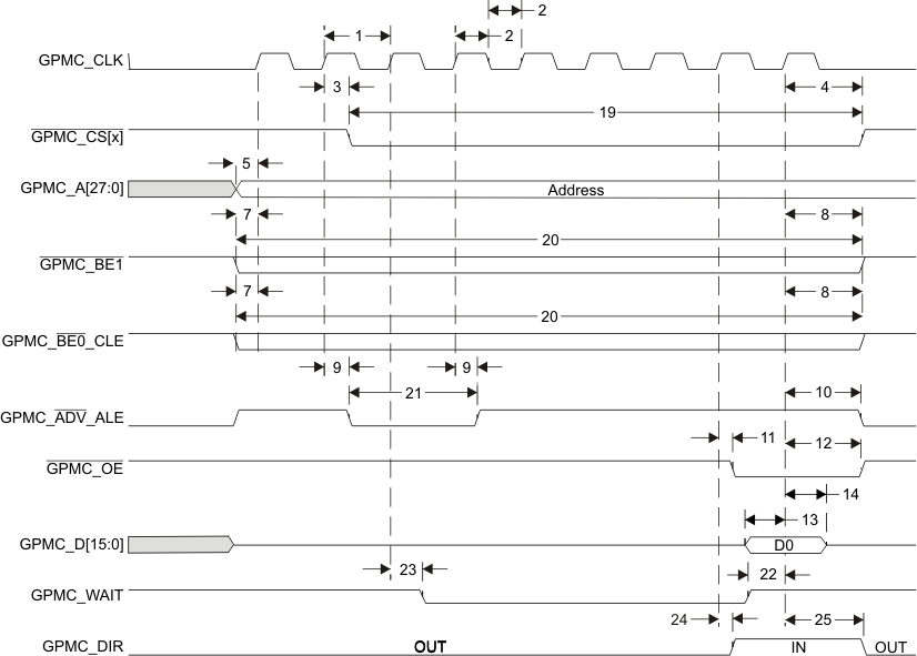 Figure 9-50 GPMC Non-Multiplexed NOR Flash - Synchronous Single Read (GPMCFCLKDIVIDER = 0)
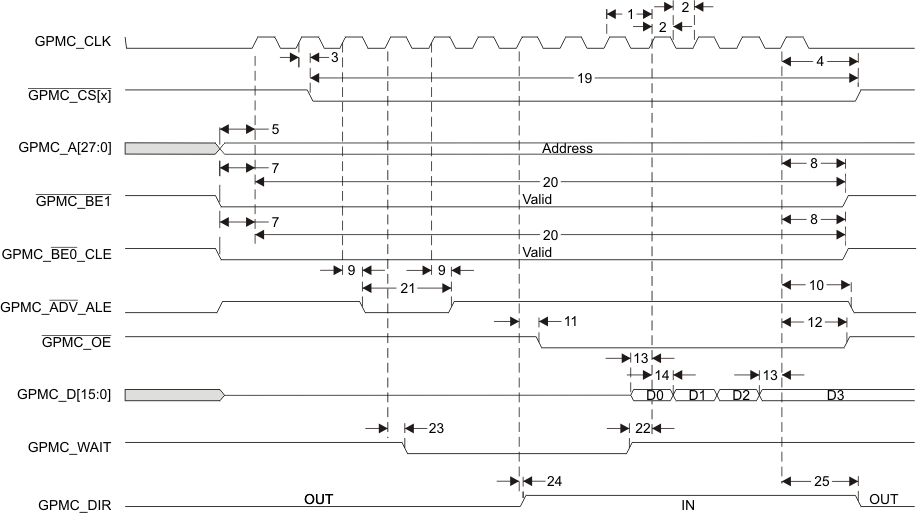 Figure 9-51 GPMC Non-Multiplexed NOR Flash - 4x16-bit Synchronous Burst Read (GPMCFCLKDIVIDER = 0)
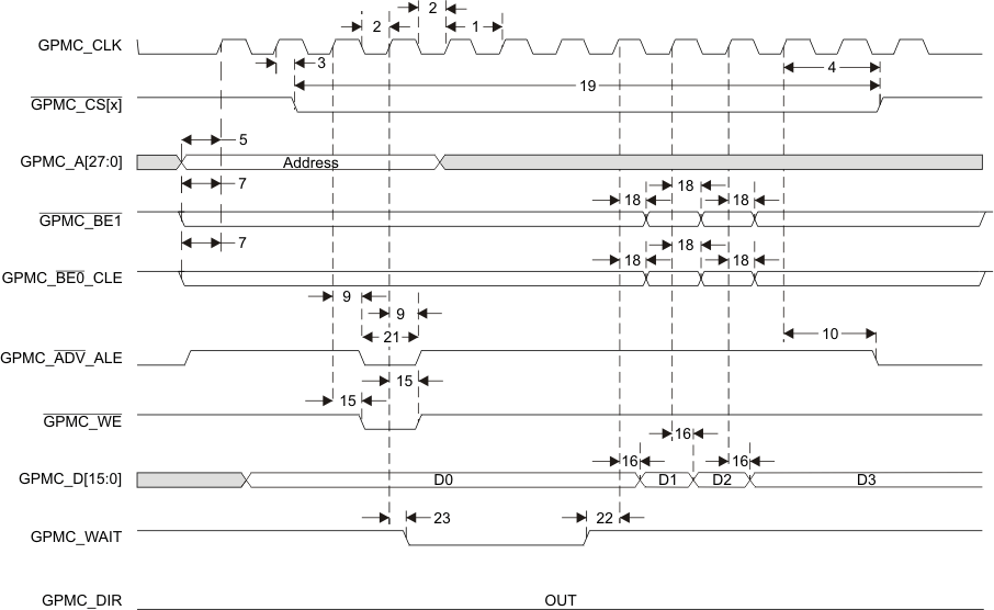 Figure 9-52 GPMC Non-Multiplexed NOR Flash - Synchronous Burst Write (GPMCFCLKDIVIDER = 0)
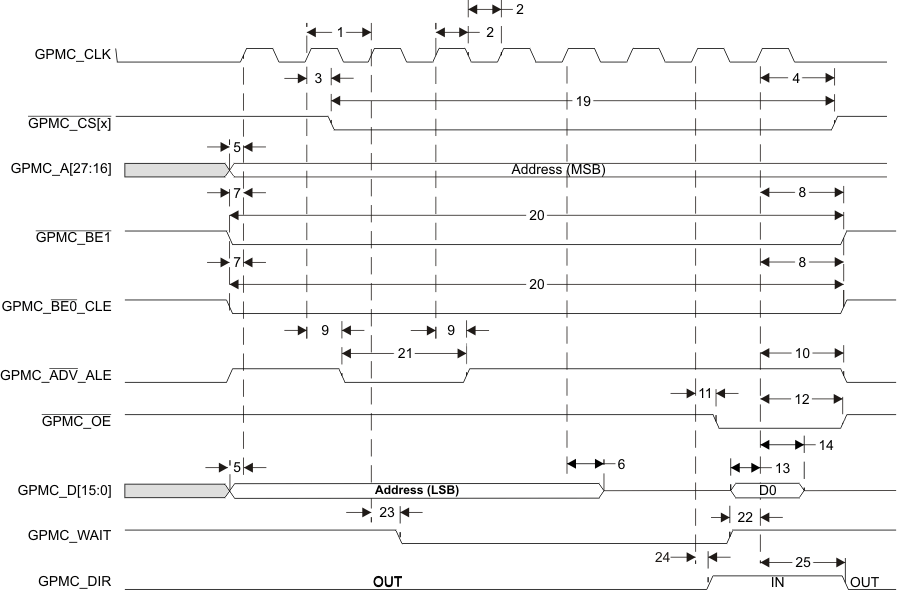 Figure 9-53 GPMC Multiplexed NOR Flash - Synchronous Single Read (GPMCFCLKDIVIDER = 0)
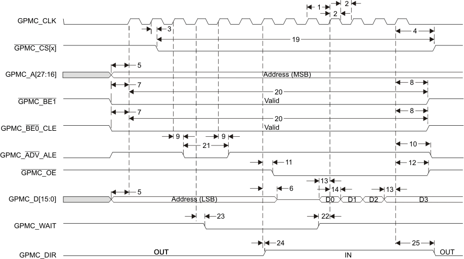 Figure 9-54 GPMC Multiplexed NOR Flash - 4x16-bit Synchronous Burst Read (GPMCFCLKDIVIDER = 0)
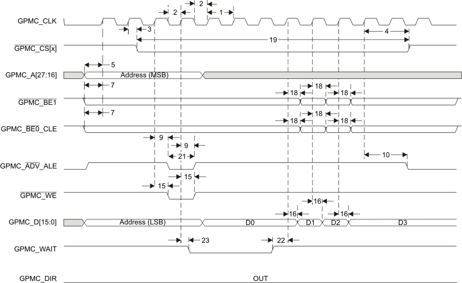 Figure 9-55 GPMC Multiplexed NOR Flash - Synchronous Burst Write (GPMCFCLKDIVIDER = 0)
9.8.2.2 GPMC and NOR Flash Interface Asynchronous Mode Timing
Table 9-56 GPMC and NOR Flash Interface Asynchronous Mode Timing - Internal Parameters
| NO. | MIN | MAX | UNIT | ||
|---|---|---|---|---|---|
| 1 | Max. output data generation delay from internal functional clock | 6.5 | ns | ||
| 2 | Max. input data capture delay by internal functional clock | 4 | ns | ||
| 3 | Max. chip select generation delay from internal functional clock | 6.5 | ns | ||
| 4 | Max. address generation delay from internal functional clock | 6.5 | ns | ||
| 5 | Max. address valid generation delay from internal functional clock | 6.5 | ns | ||
| 6 | Max. byte enable generation delay from internal functional clock | 6.5 | ns | ||
| 7 | Max. output enable generation delay from internal functional clock | 6.5 | ns | ||
| 8 | Max. write enable generation delay from internal functional clock | 6.5 | ns | ||
| 9 | Max. functional clock skew | 100 | ps | ||
Table 9-57 Timing Requirements for GPMC and NOR Flash Interface - Asynchronous Mode
(see Figure 9-56, Figure 9-57, Figure 9-58, Figure 9-60)| NO. | MIN | MAX | UNIT | ||
|---|---|---|---|---|---|
| 6 | tacc(DAT) | Data maximum access time (GPMC_FCLK cycles) | H(1) | cycles | |
| 21 | tacc1-pgmode(DAT) | Page mode successive data maximum access time (GPMC_FCLK cycles) | P(2) | cycles | |
| 22 | tacc2-pgmode(DAT) | Page mode first data maximum access time (GPMC_FCLK cycles) | H(1) | cycles | |
Table 9-58 Switching Characteristics Over Recommended Operating Conditions for GPMC and NOR Flash Interface - Asynchronous Mode
(see Figure 9-56, Figure 9-57, Figure 9-58, Figure 9-59, Figure 9-60, Figure 9-61)| NO. | PARAMETER | MIN | MAX | UNIT | |
|---|---|---|---|---|---|
| 1 | tw(nBEV) | Pulse duration, GPMC_BE0_CLE, GPMC_BE1 valid time | N(1) | ns | |
| 2 | tw(nCSV) | Pulse duration, GPMC_CS[x] low | A(2) | ns | |
| 4 | td(nCSV-nADVIV) | Delay time, GPMC_CS[x] valid to GPMC_NADV_ALE invalid | B - 0.2(3) | B + 2.0(3) | ns |
| 5 | td(nCSV-nOEIV) | Delay time, GPMC_CS[x] valid to GPMC_OE_RE invalid (single read) | C - 0.2(4) | C + 2.0(4) | ns |
| 10 | td(AV-nCSV) | Delay time, address bus valid to GPMC_CS[x] valid | J - 0.2(5) | J + 2.0(5) | ns |
| 11 | td(nBEV-nCSV) | Delay time, GPMC_BE0_CLE, GPMC_BE1 valid to GPMC_CS[x] valid | J - 0.2(5) | J + 2.0(5) | ns |
| 13 | td(nCSV-nADVV) | Delay time, GPMC_CS[x] valid to GPMC_ADV_ALE valid | K - 0.2(6) | K + 2.0(6) | ns |
| 14 | td(nCSV-nOEV) | Delay time, GPMC_CS[x] valid to GPMC_OE_RE valid | L - 0.2(7) | L + 2.0(7) | ns |
| 15 | td(nCSV-DIR) | Delay time, GPMC_CS[x] valid to GPMC_DIR high | L - 0.2(7) | L + 2.0(7) | ns |
| 16 | td(nCSV-DIR) | Delay time, GPMC_CS[x] valid to GPMC_DIR low | M - 0.2(8) | M + 2.0(8) | ns |
| 17 | tw(AIV) | Address invalid duration between 2 successive read or write accesses | G(9) | ns | |
| 19 | td(nCSV-nOEIV) | Delay time, GPMC_CS[x] valid to GPMC_OE_RE invalid (burst read) | I - 0.2(10) | I + 2.0(10) | ns |
| 21 | tw(AV) | Pulse duration, address valid: second, third and fourth accesses | D(11) | ns | |
| 26 | td(nCSV-nWEV) | Delay time, GPMC_CS[x] valid to GPMC_WE valid | E - 0.2(12) | E + 2.0(12) | ns |
| 28 | td(nCSV-nWEIV) | Delay time, GPMC_CS[x] valid to GPMC_WE invalid | F - 0.2(13) | F + 2.0(13) | ns |
| 29 | td(nWEV-DV) | Delay time, GPMC_WE valid to data bus valid | 2.0 | ns | |
| 30 | td(DV-nCSV) | Delay time, data bus valid to GPMC_CS[x] valid | J - 0.2(5) | J + 2.0(5) | ns |
| 38 | td(nOEV-AIV) | Delay time, GPMC_OE_RE valid to GPMC_A[16:1]_D[15:0] address phase end | 2.0 | ns | |
For single write: N = WrCycleTime * (TimeParaGranularity + 1) * GPMC_FCLK
For burst read: N = (RdCycleTime + (n - 1) * PageBurstAccessTime) * (TimeParaGranularity + 1) * GPMC_FCLK
For burst write: N = (WrCycleTime + (n - 1) * PageBurstAccessTime) * (TimeParaGranularity + 1) * GPMC_FCLK
For single write: A = (CSWrOffTime - CSOnTime) * (TimeParaGranularity + 1) * GPMC_FCLK
For burst read: A = (CSRdOffTime - CSOnTime + (n - 1) * PageBurstAccessTime) * (TimeParaGranularity + 1) * GPMC_FCLK
For burst write: A = (CSWrOffTime - CSOnTime + (n - 1) * PageBurstAccessTime) * (TimeParaGranularity + 1) * GPMC_FCLK
For reading: B = ((ADVRdOffTime - CSOnTime) * (TimeParaGranularity + 1) + 0.5 * (ADVExtraDelay - CSExtraDelay)) * GPMC_FCLK
For writing: B = ((ADVWrOffTime - CSOnTime) * (TimeParaGranularity + 1) + 0.5 * (ADVExtraDelay - CSExtraDelay)) * GPMC_FCLK
C = ((OEOffTime - CSOnTime) * (TimeParaGranularity + 1) + 0.5 * (OEExtraDelay - CSExtraDelay)) * GPMC_FCLK
J = (CSOnTime * (TimeParaGranularity + 1) + 0.5 * CSExtraDelay) * GPMC_FCLK
K = ((ADVOnTime - CSOnTime) * (TimeParaGranularity + 1) + 0.5 * (ADVExtraDelay - CSExtraDelay)) * GPMC_FCLK
L = ((OEOnTime - CSOnTime) * (TimeParaGranularity + 1) + 0.5 * (OEExtraDelay - CSExtraDelay)) * GPMC_FCLK
M = ((RdCycleTime - CSOnTime) * (TimeParaGranularity + 1) - 0.5 * CSExtraDelay) * GPMC_FCLK.
Parameter M expression is given as one example of GPMC programming. The IO DIR signal goes from IN to OUT after both RdCycleTime and BusTurnAround completion. Behavior of the IO direction signal depends on the kind of successive read and write accesses performed to the memory and multiplexed or non-multiplexed memory addressing scheme, whether the bus keeping feature is enabled or not. The IO DIR behavior is automatically handled by the GPMC controller.
I = ((OEOffTime + (n - 1) * PageBurstAccessTime - CSOnTime) * (TimeParaGranularity + 1) + 0.5 * (OEExtraDelay - CSExtraDelay)) * GPMC_FCLK
E = ((WEOnTime - CSOnTime) * (TimeParaGranularity + 1) + 0.5 * (WEExtraDelay - CSExtraDelay)) * GPMC_FCLK
F = ((WEOffTime - CSOnTime) * (TimeParaGranularity + 1) + 0.5 * (WEExtraDelay - CSExtraDelay)) * GPMC_FCLK
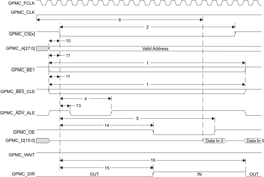 Figure 9-56 GPMC Non-Multiplexed NOR Flash - Asynchronous Read - Single Word Timing
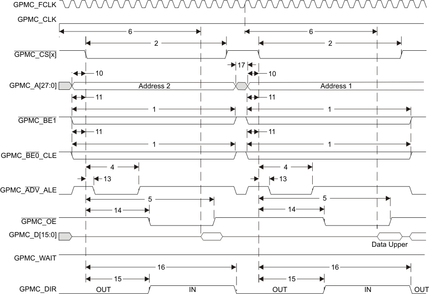 Figure 9-57 GPMC Non-Multiplexed NOR Flash - Asynchronous Read - 32-Bit Timing
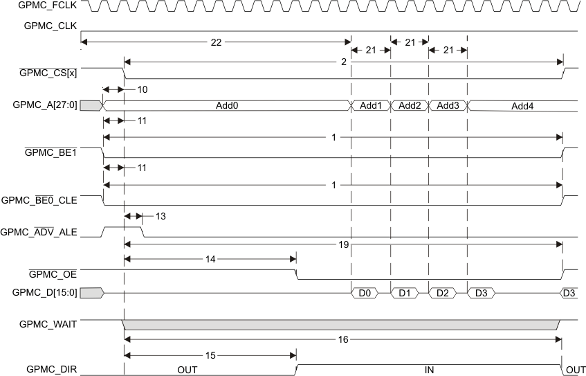 Figure 9-58 GPMC Non-Multiplexed Only NOR Flash - Asynchronous Read - Page Mode 4x16-Bit Timing
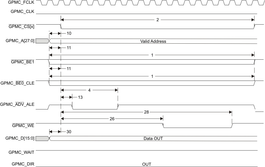 Figure 9-59 GPMC Non-Multiplexed NOR Flash - Asynchronous Write - Single Word Timing
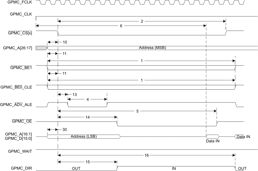 Figure 9-60 GPMC Multiplexed NOR Flash - Asynchronous Read - Single Word Timing
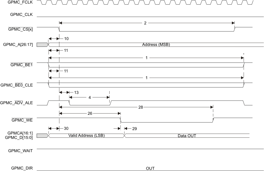 Figure 9-61 GPMC Multiplexed NOR Flash - Asynchronous Write - Single Word Timing
9.8.2.3 GPMC and NAND Flash Interface Asynchronous Mode Timing
Table 9-59 GPMC and NAND Flash Interface Asynchronous Mode Timing - Internal Parameters
| NO. | MIN | MAX | UNIT | |
|---|---|---|---|---|
| 1 | Max. output data generation delay from internal functional clock | 6.5 | ns | |
| 2 | Max. input data capture delay by internal functional clock | 4.0 | ns | |
| 3 | Max. chip select generation delay from internal functional clock | 6.5 | ns | |
| 4 | Max. address latch enable generation delay from internal functional clock | 6.5 | ns | |
| 5 | Max. command latch enable generation delay from internal functional clock | 6.5 | ns | |
| 6 | Max. output enable generation delay from internal functional clock | 6.5 | ns | |
| 7 | Max. write enable generation delay from internal functional clock | 6.5 | ns | |
| 8 | Max. functional clock skew | 100.0 | ps |
Table 9-60 Timing Requirements for GPMC and NAND Flash Interface
(see Figure 9-64)| NO. | MIN | MAX | UNIT | ||
|---|---|---|---|---|---|
| 13 | tacc(DAT) | Data maximum access time (GPMC_FCLK cycles) | J(1) | cycles | |
Table 9-61 Switching Characteristics Over Recommended Operating Conditions for GPMC and NAND Flash Interface
(see Figure 9-62, Figure 9-63, Figure 9-64, Figure 9-65)| NO. | PARAMETER | MIN | MAX | UNIT | |
|---|---|---|---|---|---|
| 1 | tw(nWEV) | Pulse duration, GPMC_WE valid time | A(1) | ns | |
| 2 | td(nCSV-nWEV) | Delay time, GPMC_CS[x] valid to GPMC_WE valid | B - 0.2(2) | B + 2.0(2) | ns |
| 3 | td(CLEH-nWEV) | Delay time, GPMC_BE0_CLE high to GPMC_WE valid | C - 0.2(3) | C + 2.0(3) | ns |
| 4 | td(nWEV-DV) | Delay time, GPMC_D[15:0] valid to GPMC_WE valid | D - 0.2(4) | D + 2.0(4) | ns |
| 5 | td(nWEIV-DIV) | Delay time, GPMC_WE invalid to GPMC_D[15:0] invalid | E - 0.2(5) | E + 2.0(5) | ns |
| 6 | td(nWEIV-CLEIV) | Delay time, GPMC_WE invalid to GPMC_BE0_CLE invalid | F - 0.2(6) | F + 2.0(6) | ns |
| 7 | td(nWEIV-nCSIV) | Delay time, GPMC_WE invalid to GPMC_CS[x] invalid | G - 0.2(7) | G + 2.0(7) | ns |
| 8 | td(ALEH-nWEV) | Delay time, GPMC_ADV_ALE High to GPMC_WE valid | C - 0.2(3) | C + 2.0(3) | ns |
| 9 | td(nWEIV-ALEIV) | Delay time, GPMC_WE invalid to GPMC_ADV_ALE invalid | F - 0.2(6) | F + 2.0(6) | ns |
| 10 | tc(nWE) | Cycle time, write cycle time | H(8) | ns | |
| 11 | td(nCSV-nOEV) | Delay time, GPMC_CS[x] valid to GPMC_OE_RE valid | I - 0.2(9) | I + 2.0(9) | ns |
| 12 | tw(nOEV) | Pulse duration, GPMC_OE_RE valid time | K(10) | ns | |
| 13 | tc(nOE) | Cycle time, read cycle time | L(11) | ns | |
| 14 | td(nOEIV-nCSIV) | Delay time, GPMC_OE_RE invalid to GPMC_CS[x] invalid | M - 0.2(12) | M + 2.0(12) | ns |
B = ((WEOnTime - CSOnTime) * (TimeParaGranularity + 1) + 0.5 * (WEExtraDelay - CSExtraDelay)) * GPMC_FCLK
C = ((WEOnTime - ADVOnTime) * (TimeParaGranularity + 1) + 0.5 * (WEExtraDelay - ADVExtraDelay)) * GPMC_FCLK
D = (WEOnTime * (TimeParaGranularity + 1) + 0.5 * WEExtraDelay ) * GPMC_FCLK
E = ((WrCycleTime - WEOffTime) * (TimeParaGranularity + 1) - 0.5 * WEExtraDelay ) * GPMC_FCLK
F = ((ADVWrOffTime - WEOffTime) * (TimeParaGranularity + 1) + 0.5 * (ADVExtraDelay - WEExtraDelay )) * GPMC_FCLK
G = ((CSWrOffTime - WEOffTime) * (TimeParaGranularity + 1) + 0.5 * (CSExtraDelay - WEExtraDelay )) * GPMC_FCLK
I = ((OEOnTime - CSOnTime) * (TimeParaGranularity + 1) + 0.5 * (OEExtraDelay - CSExtraDelay)) * GPMC_FCLK
M = ((CSRdOffTime - OEOffTime) * (TimeParaGranularity + 1) + 0.5 * (CSExtraDelay - OEExtraDelay ))* GPMC_FCLK
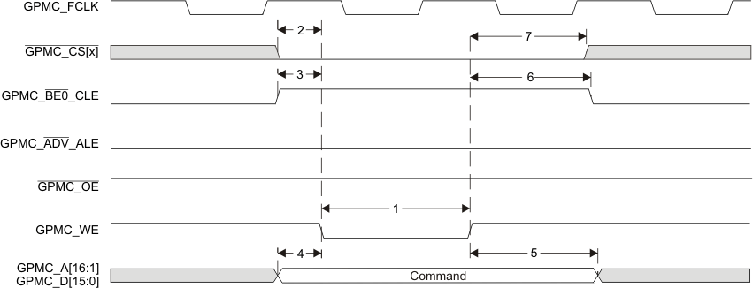 Figure 9-62 GPMC and NAND Flash - Command Latch Cycle Timing
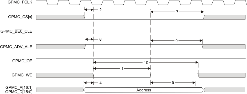 Figure 9-63 GPMC and NAND Flash - Address Latch Cycle Timing
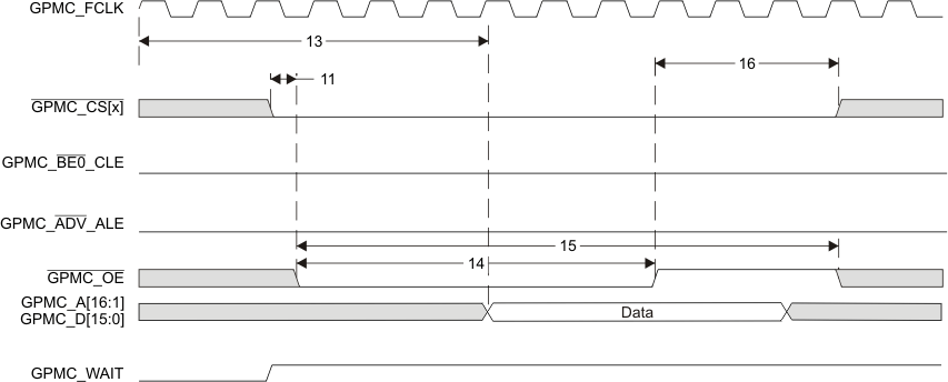 Figure 9-64 GPMC and NAND Flash - Data Read Cycle Timing
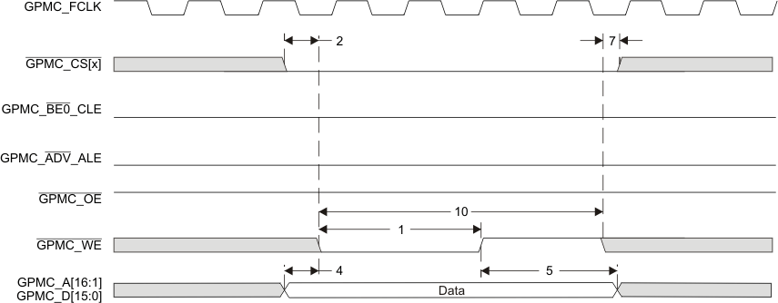 Figure 9-65 GPMC and NAND Flash - Data Write Cycle Timing
9.9 High-Definition Multimedia Interface (HDMI)
The device includes an HDMI 1.3a-compliant transmitter for digital video and audio data to display devices. The HDMI interface consists of a digital HDMI transmitter core with TMDS encoder, a core wrapper with interface logic and control registers, and a transmit PHY, with the following features:
- Hot-plug detection
- Consumer electronics control (CEC) messages
- DVI 1.0 compliant (only RGB pixel format)
- CEA 861-D and VESA DMT formats
- Supports up to 165-MHz pixel clock:
- 1920 x 1080p @75 Hz with 8-bit component color depth
- 1920 x 1200 @60 Hz with 8-bit component color depth
- 1600 x 1200 @60 Hz with 8-bit component color depth
- Support for deep-color mode:
- 10-bit component color depth up to 1080p @60 Hz (maximum pixel clock = 148.5 MHz)
- 12-bit component color depth at 720p or 1080i @60 Hz (maximum pixel clock = 123.75 MHz)
- Uncompressed multichannel (up to eight channels) audio (L-PCM) support
- Master I2C interface for display data channel (DDC) connection
- TMDS clock to the HDMI-PHY is up to 185.625 MHz
- Maximum supported pixel clock:
- 165 MHz for 8-bit color depth
- 148.5 MHz for 10-bit color depth
- 123.75 MHz for 12-bit color depth
- Options available to support HDCP encryption engine for transmitting protected audio and video (contact local TI sales representative for information).
For more details on the HDMI, see the HDMI chapter in the TMS320DM816x DaVinci Digital Media Processors Technical Reference Manual (literature number SPRUGX8).
9.9.1 HDMI Interface Design Specifications
NOTE
For more information on PCB layout, see the DM816xx Easy CYG Package PCB Escape Routing application report (literature number SPRABK6).
This section provides PCB design and layout specifications for the HDMI interface. The design rules constrain PCB trace length, PCB trace skew, signal integrity, cross-talk, and signal timing. Simulation and system design work has been done to ensure the HDMI interface requirements are met.
9.9.1.1 HDMI Interface Schematic
The HDMI bus is separated into three main sections:
- Transition Minimized Differential Signaling (TMDS) high-speed digital video interface
- Display Data Channel (I2C bus for configuration and status exchange between two devices)
- Consumer Electronics Control (optional) for remote control of connected devices.
The DDC and CEC are low-speed interfaces, so nothing special is required for PCB layout of these signals. Their connection is shown in Figure 9-66.
The TMDS channels are high-speed differential pairs and, therefore, require the most care in layout. Specifications for TMDS layout are below.
Figure 9-66 shows the HDMI interface schematic. The specific pin numbers can be obtained from Table 4-7, HDMI Terminal Functions.
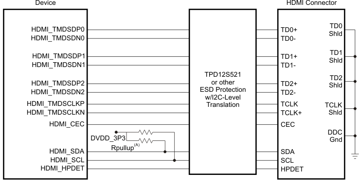
9.9.1.2 TMDS Routing
The TMDS signals are high-speed differential pairs. Care must be taken in the PCB layout of these signals to ensure good signal integrity.
The TMDS differential signal traces must be routed to achieve 100 Ω (±10%) differential impedance and 60 Ω (±10%) single-ended impedance. Single-ended impedance control is required because differential signals are extremely difficult to closely couple on PCBs and, therefore, single-ended impedance becomes important.
These impedances are impacted by trace width, trace spacing, distance to reference planes, and dielectric material. Verify with a PCB design tool that the trace geometry for both data signal pairs results in as close to 60 Ω impedance traces as possible. For best accuracy, work with your PCB fabricator to ensure this impedance is met.
In general, closely coupled differential signal traces are not an advantage on PCBs. When differential signals are closely coupled, tight spacing and width control is necessary. Very small width and spacing variations affect impedance dramatically, so tight impedance control can be more problematic to maintain in production.
Loosely coupled PCB differential signals make impedance control much easier. Wider traces and spacing make obstacle avoidance easier, and trace width variations do not affect impedance as much; therefore, it is easier to maintain an accurate impedance over the length of the signal. The wider traces also show reduced skin effect and, therefore, often result in better signal integrity.
Table 9-62 shows the routing specifications for the TMDS signals.
Table 9-62 TMDS Routing Specifications
| PARAMETER | MIN | TYP | MAX | UNIT |
|---|---|---|---|---|
| Processor-to-HDMI header trace length | 7000 | Mils | ||
| Number of stubs allowed on TMDS traces | 0 | Stubs | ||
| TX and RX pair differential impedance | 90 | 100 | 110 | Ω |
| TX and RX single-ended impedance | 54 | 60 | 66 | Ω |
| Number of vias on each TMDS trace | 2 | Vias(1) | ||
| TMDS differential pair to any other trace spacing | 2*DS(2) |
9.9.1.3 DDC Signals
As shown in Figure 9-66, the DDC connects just like a standard I2C bus. As such, resistor pullups must be used to pull up the open drain buffer signals unless they are integrated into the ESD protection chip used. If used, these pullup resistors should be connected to a 3.3-V supply.
9.9.1.4 HDMI ESD Protection Device (Required)
Interfaces that connect to a cable such as HDMI generally require more ESD protection than can be built into the processor's outputs. Therefore, this HDMI interface requires the use of an ESD protection chip to provide adequate ESD protection and to translate I2C voltage levels from the 3.3 V supplied by the device to the 5 volts required by the HDMI specification.
When selecting an ESD protection chip, choose the lowest capacitance ESD protection available to minimize signal degradation. In no case should the ESD protection circuit capacitance be more than 5 pF.
TI manufactures devices that provide ESD protection for HDMI signals such as the TPD12S521. For more information see the www.ti.com website.
9.9.1.5 PCB Stackup Specifications
Table 9-63 shows the stackup and feature sizes required for HDMI.
Table 9-63 HDMI PCB Stackup Specifications
| PARAMETER | MIN | TYP | MAX | UNIT |
|---|---|---|---|---|
| PCB routing and plane layers | 4 | 6 | - | Layers |
| Signal routing layers | 2 | 3 | - | Layers |
| Number of ground plane cuts allowed within HDMI routing region | - | - | 0 | Cuts |
| Number of layers between HDMI routing region and reference ground plane | - | - | 0 | Layers |
| PCB trace width | - | 4 | - | Mils |
| PCB BGA escape via pad size | - | 20 | - | Mils |
| PCB BGA escape via hole size | - | 10 | Mils | |
| Processor device BGA pad size(1)(2) | 0.3 | mm |
9.9.1.6 Grounding
Each TMDS channel has its own shield pin which should be grounded to provide a return current path for the TMDS signal.
9.9.2 HDMI Peripheral Register Descriptions
Table 9-64 HDMI Wrapper Registers
| HEX ADDRESS | ACRONYM | REGISTER NAME |
|---|---|---|
| 0x46C0 0000 | HDMI_WP_REVISION | IP Revision Identifier |
| 0x46C0 0010 | HDMI_WP_SYSCONFIG | Clock Management Configuration |
| 0x46C0 0024 | HDMI_WP_IRQSTATUS_RAW | Raw Interrupt Status |
| 0x46C0 0028 | HDMI_WP_IRQSTATUS | Interrupt Status |
| 0x46C0 002C | HDMI_WP_IRQENABLE_SET | Interrupt Enable |
| 0x46C0 0030 | HDMI_WP_IRQENABLE_CLR | Interrupt Disable |
| 0x46C0 0034 | HDMI_WP_IRQWAKEEN | IRQ Wakeup |
| 0x46C0 0050 | HDMI_WP_VIDEO_CFG | Configuration of HDMI Wrapper Video |
| 0x46C0 0070 | HDMI_WP_CLK | Configuration of Clocks |
| 0x46C0 0080 | HDMI_WP_AUDIO_CFG | Audio Configuration in FIFO |
| 0x46C0 0084 | HDMI_WP_AUDIO_CFG2 | Audio Configuration of DMA |
| 0x46C0 0088 | HDMI_WP_AUDIO_CTRL | Audio FIFO Control |
| 0x46C0 008C | HDMI_WP_AUDIO_DATA | TX Data of FIFO |
Table 9-65 HDMI Core System Registers
| HEX ADDRESS | ACRONYM | REGISTER NAME |
|---|---|---|
| 0x46C0 0400 | VND_IDL | Vendor ID |
| 0x46C0 0404 | VND_IDH | Vendor ID |
| 0x46C0 0408 | DEV_IDL | Device ID |
| 0x46C0 040C | DEV_IDH | Device ID |
| 0x46C0 0410 | DEV_REV | Device Revision |
| 0x46C0 0414 | SRST | Software Reset |
| 0x46C0 0420 | SYS_CTRL1 | System Control 1 |
| 0x46C0 0424 | SYS_STAT | System Status |
| 0x46C0 0428 | SYS_CTRL3 | Legacy |
| 0x46C0 0434 | DCTL | Data Control |
| 0x46C0 043C - 0x46C0 0494 | - | Reserved |
| 0x46C0 0498 | RI_STAT | Ri Status |
| 0x46C0 049C | RI_CMD | Ri Command |
| 0x46C0 04A0 | RI_START | Ri Line Start |
| 0x46C0 04A4 | RI_RX_L | Ri From RX |
| 0x46C0 04A8 | RI_RX_H | Ri From RX |
| 0x46C0 04AC | RI_DEBUG | Ri Debug |
| 0x46C0 04C8 | DE_DLY | VIDEO DE Delay |
| 0x46C0 04C8 | DE_DLY | VIDEO DE Delay |
| 0x46C0 04CC | DE_CTRL | VIDEO DE Control |
| 0x46C0 04D0 | DE_TOP | VIDEO DE Top |
| 0x46C0 04D8 | DE_CNTL | VIDEO DE Count |
| 0x46C0 04DC | DE_CNTH | VIDEO DE Count |
| 0x46C0 04E0 | DE_LINL | VIDEO DE Line |
| 0x46C0 04E4 | DE_LINH_1 | VIDEO DE Line |
| 0x46C0 04E8 | HRES_L | Video H Resolution |
| 0x46C0 04EC | HRES_H | Video H Resolution |
| 0x46C0 04F0 | VRES_L | Video V Resolution |
| 0x46C0 04F4 | VRES_H | Video V Resolution |
| 0x46C0 04F8 | IADJUST | Video Interlace Adjustment |
| 0x46C0 04FC | POL_DETECT | Video SYNC Polarity Detection |
| 0x46C0 0500 | HBIT_2HSYNC1 | Video Hbit to HSYNC |
| 0x46C0 0504 | HBIT_2HSYNC2 | Video Hbit to HSYNC |
| 0x46C0 0508 | FLD2_HS_OFSTL | Video Field2 HSYNC Offset |
| 0x46C0 050C | FLD2_HS_OFSTH | Video Field2 HSYNC Offset |
| 0x46C0 0510 | HWIDTH1 | Video HSYNC Length |
| 0x46C0 0514 | HWIDTH2 | Video HSYNC Length |
| 0x46C0 0518 | VBIT_TO_VSYNC | Video Vbit to VSYNC |
| 0x46C0 051C | VWIDTH | Video VSYNC Length |
| 0x46C0 0520 | VID_CTRL | Video Control |
| 0x46C0 0524 | VID_ACEN | Video Action Enable |
| 0x46C0 0528 | VID_MODE | Video Mode1 |
| 0x46C0 052C | VID_BLANK1 | Video Blanking |
| 0x46C0 0530 | VID_BLANK2 | Video Blanking |
| 0x46C0 0534 | VID_BLANK3 | Video Blanking |
| 0x46C0 0538 | DC_HEADER | Deep Color Header |
| 0x46C0 053C | VID_DITHER | Video Mode2 |
| 0x46C0 0540 | RGB2XVYCC_CT | RGB_2_xvYCC control |
| 0x46C0 0544 | R2Y_COEFF_LOW | RGB_2_xvYCC Conversion R_2_Y |
| 0x46C0 0548 | R2Y_COEFF_UP | RGB_2_xvYCC Conversion R_2_Y |
| 0x46C0 054C | G2Y_COEFF_LOW | RGB_2_xvYCC Conversion G_2_Y |
| 0x46C0 0550 | G2Y_COEFF_UP | RGB_2_xvYCC Conversion G_2_Y |
| 0x46C0 0554 | B2Y_COEFF_LOW | RGB_2_xvYCC Conversion B_2_Y |
| 0x46C0 0558 | B2Y_COEFF_UP | RGB_2_xvYCC Conversion B_2_Y |
| 0x46C0 055C | R2CB_COEFF_LOW | RGB_2_xvYCC Conversion R_2_Cb |
| 0x46C0 0560 | R2CB_COEFF_UP | RGB_2_xvYCC Conversion R_2_Cb |
| 0x46C0 0564 | G2CB_COEFF_LOW | RGB_2_xvYCC Conversion G_2_Cb |
| 0x46C0 0568 | G2CB_COEFF_UP | RGB_2_xvYCC Conversion G_2_Cb |
| 0x46C0 056C | B2CB_COEFF_LOW | RGB_2_xvYCC Conversion B_2_Cb |
| 0x46C0 0570 | B2CB_COEFF_UP | RGB_2_xvYCC Conversion B_2_Cb |
| 0x46C0 0574 | R2CR_COEFF_LOW | RGB_2_xvYCC Conversion R_2_Cr |
| 0x46C0 0578 | R2CR_COEFF_UP | RGB_2_xvYCC Conversion R_2_Cr |
| 0x46C0 057C | G2CR_COEFF_LOW | RGB_2_xvYCC Conversion G_2_Cr |
| 0x46C0 0580 | G2CR_COEFF_UP | RGB_2_xvYCC Conversion G_2_Cr |
| 0x46C0 0584 | B2CR_COEFF_LOW | RGB_2_xvYCC Conversion B_2_Cr |
| 0x46C0 0588 | B2CR_COEFF_UP | RGB_2_xvYCC Conversion B_2_Cr |
| 0x46C0 058C | RGB_OFFSET_LOW | RGB_2_xvYCC RGB Input Offset |
| 0x46C0 0590 | RGB_OFFSET_UP | RGB_2_xvYCC RGB Input Offset |
| 0x46C0 0594 | Y_OFFSET_LOW | RGB_2_xvYCC Conversion Y Output Offset |
| 0x46C0 0598 | Y_OFFSET_UP | RGB_2_xvYCC Conversion Y Output Offset |
| 0x46C0 059C | CBCR_OFFSET_LOW | RGB_2_xvYCC Conversion CbCr Output Offset |
| 0x46C0 05A0 | CBCR_OFFSET_UP | RGB_2_xvYCC Conversion CbCr Output Offset |
| 0x46C0 05C0 | INTR_STATE | Interrupt State |
| 0x46C0 05C4 | INTR1 | Interrupt Source |
| 0x46C0 05C8 | INTR2 | Interrupt Source |
| 0x46C0 05CC | INTR3 | Interrupt Source |
| 0x46C0 05D0 | INTR4 | Interrupt Source |
| 0x46C0 05D4 | INT_UNMASK1 | Interrupt Unmask |
| 0x46C0 05D8 | INT_UNMASK2 | Interrupt Unmask |
| 0x46C0 05DC | INT_UNMASK3 | Interrupt Unmask |
| 0x46C0 05E0 | INT_UNMASK4 | Interrupt Unmask |
| 0x46C0 05E4 | INT_CTRL | Interrupt Control |
| 0x46C0 0640 | XVYCC2RGB_CTL | xvYCC_2_RGB Control |
| 0x46C0 0644 | Y2R_COEFF_LOW | xvYCC_2_RGB Conversion Y_2_R |
| 0x46C0 0648 | Y2R_COEFF_UP | xvYCC_2_RGB Conversion Y_2_R |
| 0x46C0 064C | CR2R_COEFF_LOW | xvYCC_2_RGB Conversion Cr_2_R |
| 0x46C0 0650 | CR2R_COEFF_UP | xvYCC_2_RGB Conversion Cr_2_R |
| 0x46C0 0654 | CB2B_COEFF_LOW | xvYCC_2_RGB Conversion Cb_2_B |
| 0x46C0 0658 | CB2B_COEFF_UP | xvYCC_2_RGB Conversion Cb_2_B |
| 0x46C0 065C | CR2G_COEFF_LOW | xvYCC_2_RGB Conversion Cr_2_G |
| 0x46C0 0660 | CR2G_COEFF_UP | xvYCC_2_RGB Conversion Cr_2_G |
| 0x46C0 0664 | CB2G_COEFF_LOW | xvYCC_2_RGB Conversion Cb_2_G |
| 0x46C0 0668 | CB2G_COEFF_UP | xvYCC_2_RGB Conversion Cb_2_G |
| 0x46C0 066C | YOFFSET1_LOW | xvYCC_2_RGB Conversion Y Offset |
| 0x46C0 0670 | YOFFSET1_UP | xvYCC_2_RGB Conversion Y Offset |
| 0x46C0 0674 | OFFSET1_LOW | xvYCC_2_RGB Conversion Offset1 |
| 0x46C0 0678 | OFFSET1_MID | xvYCC_2_RGB Conversion Offset1 |
| 0x46C0 067C | OFFSET1_UP | xvYCC_2_RGB Conversion Offset1 |
| 0x46C0 0680 | OFFSET2_LOW | xvYCC_2_RGB Conversion Offset2 |
| 0x46C0 0684 | OFFSET2_UP | xvYCC_2_RGB Conversion Offset2 |
| 0x46C0 0688 | DCLEVEL_LOW | xvYCC_2_RGB Conversion DC Level |
| 0x46C0 068C | DCLEVEL_UP | xvYCC_2_RGB Conversion DC Level |
| 0x46C0 07B0 | DDC_MAN | DDC I2C Manual |
| 0x46C0 07B4 | DDC_ADDR | DDC I2C Target Slave Address |
| 0x46C0 07B8 | DDC_SEGM | DDC I2C Target Segment Address |
| 0x46C0 07BC | DDC_OFFSET | DDC I2C Target Offset Address |
| 0x46C0 07C0 | DDC_COUNT1 | DDC I2C Data Count |
| 0x46C0 07C4 | DDC_COUNT2 | DDC I2C Data Count |
| 0x46C0 07C8 | DDC_STATUS | DDC I2C Status |
| 0x46C0 07CC | DDC_CMD | DDC I2C Command |
| 0x46C0 07D0 | DDC_DATA | DDC I2C Data |
| 0x46C0 07D4 | DDC_FIFOCNT | DDC I2C FIFO Count |
| 0x46C0 07E4 | EPST | ROM Status |
| 0x46C0 07E8 | EPCM | ROM Command |
Table 9-66 HDMI IP Core Gamut Registers
| HEX ADDRESS | ACRONYM | REGISTER NAME |
|---|---|---|
| 0x46C0 0800 | GAMUT_HEADER1 | Gamut Metadata |
| 0x46C0 0804 | GAMUT_HEADER2 | Gamut Metadata |
| 0x46C0 0808 | GAMUT_HEADER3 | Gamut Metadata |
| 0x46C0 080C - 0x46C0 0878 (0x4 byte increments) |
GAMUT_DBYTE__0 - GAMUT_DBYTE__27 | Gamut Metadata |
Table 9-67 HDMI IP Core Audio Video Registers
| HEX ADDRESS | ACRONYM | REGISTER NAME |
|---|---|---|
| 0x46C0 0904 | ACR_CTRL | ACR Control |
| 0x46C0 0908 | FREQ_SVAL | ACR Audio Frequency |
| 0x46C0 090C | N_SVAL1 | ACR N Software Value |
| 0x46C0 0910 | N_SVAL2 | ACR N Software Value |
| 0x46C0 0914 | N_SVAL3 | ACR N Software Value |
| 0x46C0 0918 | CTS_SVAL1 | ACR CTS Software Value |
| 0x46C0 091C | CTS_SVAL2 | ACR CTS Software Value |
| 0x46C0 0920 | CTS_SVAL3 | ACR CTS Software Value |
| 0x46C0 0924 | CTS_HVAL1 | ACR CTS Hardware Value |
| 0x46C0 0928 | CTS_HVAL2 | ACR CTS Hardware Value |
| 0x46C0 092C | CTS_HVAL3 | ACR CTS Hardware Value |
| 0x46C0 0950 | AUD_MODE | Audio In Mode |
| 0x46C0 0954 | SPDIF_CTRL | Audio In SPDIF Control |
| 0x46C0 0960 | HW_SPDIF_FS | Audio In SPDIF Extracted Fs and Length |
| 0x46C0 0964 | SWAP_I2S | Audio In I2S Channel Swap |
| 0x46C0 096C | SPDIF_ERTH | Audio Error Threshold |
| 0x46C0 0970 | I2S_IN_MAP | Audio In I2S Data In Map |
| 0x46C0 0974 | I2S_IN_CTRL | Audio In I2S Control |
| 0x46C0 0978 | I2S_CHST0 | Audio In I2S Channel Status |
| 0x46C0 097C | I2S_CHST1 | Audio In I2S Channel Status |
| 0x46C0 0980 | I2S_CHST2 | Audio In I2S Channel Status |
| 0x46C0 0984 | I2S_CHST4 | Audio In I2S Channel Status |
| 0x46C0 0988 | I2S_CHST5 | Audio In I2S Channel Status |
| 0x46C0 098C | ASRC | Audio Sample Rate Conversion |
| 0x46C0 0990 | I2S_IN_LEN | Audio I2S Input Length |
| 0x46C0 09BC | HDMI_CTRL | HDMI Control |
| 0x46C0 09C0 | AUDO_TXSTAT | Audio Path Status |
| 0x46C0 09CC | AUD_PAR_BUSCLK_1 | Audio Input Data Rate Adjustment |
| 0x46C0 09D0 | AUD_PAR_BUSCLK_2 | Audio Input Data Rate Adjustment |
| 0x46C0 09D4 | AUD_PAR_BUSCLK_3 | Audio Input Data Rate Adjustment |
| 0x46C0 09F0 | TEST_TXCTRL | Test Control |
| 0x46C0 09F4 | DPD | Diagnostic Power Down |
| 0x46C0 09F8 | PB_CTRL1 | Packet Buffer Control 1 |
| 0x46C0 09FC | PB_CTRL2 | Packet Buffer Control 2 |
| 0x46C0 0A00 | AVI_TYPE | Packet |
| 0x46C0 0A04 | AVI_VERS | Packet |
| 0x46C0 0A08 | AVI_LEN | Packet |
| 0x46C0 0A0C | AVI_CHSUM | Packet |
| 0x46C0 0A10 - 0x46C0 0A48 (0x4 byte increments) |
AVI_DBYTE__0 - AVI_DBYTE__14 | Packet |
| 0x46C0 0A80 | SPD_TYPE | SPD InfoFrame |
| 0x46C0 0A84 | SPD_VERS | SPD InfoFrame |
| 0x46C0 0A88 | SPD_LEN | SPD InfoFrame |
| 0x46C0 0A8C | SPD_CHSUM | SPD InfoFrame |
| 0x46C0 0A90 - 0x46C0 0AF8 (0x4 byte increments) |
SPD_DBYTE__0 - SPD_DBYTE__26 | SPD InfoFrame |
| 0x46C0 0B00 | AUDIO_TYPE | Audio InfoFrame |
| 0x46C0 0B04 | AUDIO_VERS | Audio InfoFrame |
| 0x46C0 0B08 | AUDIO_LEN | Audio InfoFrame |
| 0x46C0 0B0C | AUDIO_CHSUM | Audio InfoFrame |
| 0x46C0 0B10 - 0x46C0 0B34 (0x4 byte increments) |
AUDIO_DBYTE__0 - AUDIO_DBYTE__9 | Audio InfoFrame |
| 0x46C0 0B80 | MPEG_TYPE | MPEG InfoFrame |
| 0x46C0 0B84 | MPEG_VERS | MPEG InfoFrame |
| 0x46C0 0B88 | MPEG_LEN | MPEG InfoFrame |
| 0x46C0 0B8C | MPEG_CHSUM | MPEG InfoFrame |
| 0x46C0 0B90 - 0x46C0 0BF8 (0x4 byte increments) |
MPEG_DBYTE__0 - MPEG_DBYTE__26 | MPEG InfoFrame |
| 0x46C0 0C00 - 0x46C0 0C78 (0x4 byte increments) |
GEN_DBYTE__0 - GEN_DBYTE__30 | Generic Packet |
| 0x46C0 0C7C | CP_BYTE1 | General Control Packet |
| 0x46C0 0C80 - 0x46C0 0CF8 (0x4 byte increments) |
GEN2_DBYTE__0 - GEN2_DBYTE__30 | Generic Packet 2 |
| 0x46C0 0CFC | CEC_ADDR_ID | CEC Slave ID |
Table 9-68 HDMI IP Core CEC Registers
| HEX ADDRESS | ACRONYM | REGISTER NAME |
|---|---|---|
| 0x46C0 0D00 | CEC_DEV_ID | CEC Device ID |
| 0x46C0 0D04 | CEC_SPEC | CEC Specification |
| 0x46C0 0D08 | CEC_SUFF | CEC Specification Suffix |
| 0x46C0 0D0C | CEC_FW | CEC Firmware Revision |
| 0x46C0 0D10 | CEC_DBG_0 | CEC Debug 0 |
| 0x46C0 0D14 | CEC_DBG_1 | CEC Debug 1 |
| 0x46C0 0D18 | CEC_DBG_2 | CEC Debug 2 |
| 0x46C0 0D1C | CEC_DBG_3 | CEC Debug 3 |
| 0x46C0 0D20 | CEC_TX_INIT | CEC Tx Initialization |
| 0x46C0 0D24 | CEC_TX_DEST | CEC Tx Destination |
| 0x46C0 0D38 | CEC_SETUP | CEC Set Up |
| 0x46C0 0D3C | CEC_TX_COMMAND | CEC Tx Command |
| 0x46C0 0D40 - 0x46C0 0D78 (0x4 byte increments) |
CEC_TX_OPERAND__0 - CEC_TX_OPERAND__14 | CEC Tx Operand |
| 0x46C0 0D7C | CEC_TRANSMIT_DATA | CEC Transmit Data |
| 0x46C0 0D88 | CEC_CA_7_0 | CEC Capture ID0 |
| 0x46C0 0D8C | CEC_CA_15_8 | CEC Capture ID0 |
| 0x46C0 0D90 | CEC_INT_ENABLE_0 | CEC Interrupt Enable 0 |
| 0x46C0 0D94 | CEC_INT_ENABLE_1 | CEC Interrupt Enable 1 |
| 0x46C0 0D98 | CEC_INT_STATUS_0 | CEC Interrupt Status 0 |
| 0x46C0 0D9C | CEC_INT_STATUS_1 | CEC Interrupt Status 1 |
| 0x46C0 0DB0 | CEC_RX_CONTROL | CEC RX Control |
| 0x46C0 0DB4 | CEC_RX_COUNT | CEC Rx Count |
| 0x46C0 0DB8 | CEC_RX_CMD_HEADER | CEC Rx Command Header |
| 0x46C0 0DBC | CEC_RX_COMMAND | CEC Rx Command |
| 0x46C0 0DC0 - 0x46C0 0DF8 (0x4 byte increments) |
CEC_RX_OPERAND__0 - CEC_RX_OPERAND__14 | CEC Rx Operand |
Table 9-69 HDMI PHY Registers
| HEX ADDRESS | ACRONYM | REGISTER NAME |
|---|---|---|
| 0x4812 2004 | TMDS_CNTL2 | TMDS Control |
| 0x4812 2008 | TMDS_CNTL3 | TMDS Control |
| 0x4812 200C | BIST_CNTL | BIST Control |
| 0x4812 2020 | TMDS_CNTL9 | TMDS Control |
9.10 High-Definition Video Processing Subsystem (HDVPSS)
The device High-Definition Video Processing Subsystem (HDVPSS) provides a video input interface for external imaging peripherals (that is, image sensors, video decoders, and others) and a video output interface for display devices, such as analog SDTV displays, analog and digital HDTV displays, and digital LCD panels. It includes HD and SD video encoders, and an HDMI transmitter interface.
The device HDVPSS features include:
- High quality (HD) and medium quality (SD) display processing pipelines with de-interlacing, scaling, noise reduction, alpha blending, chroma keying, color space conversion, flicker filtering, and pixel format conversion.
- HD and SD compositor features for PIP support.
- Format conversions (up to 1080p 60 Hz) include scan format conversion, scan rate conversion, aspect-ratio conversion, and frame size conversion.
- Supports additional video processing capabilities by using the subsystem's memory-to-memory feature.
- Two parallel video processing pipelines support HD (up to 1080p60) and SD (NTSC and PAL) simultaneous outputs.
- HD analog component output with OSD and embedded timing codes (BT.1120)
- 3-channel HD-DAC with 12-bit resolution.
- External HSYNC and VSYNC signals available on silicon revision 2.x devices. For more details, see below.
- SD analog output with OSD with embedded timing codes (BT.656)
- Simultaneous component, S-video and composite
- 4-channel SD-DAC with 10-bit resolution
- Options available to support MacroVision and CGMS-A (contact local TI Sales rep for information).
- Digital HDMI 1.3a compliant transmitter (for details, see Section 9.9, High-Definition Multimedia Interface (HDMI)).
- HD analog component output with OSD and embedded timing codes (BT.1120)
- Up to two (one 16-bit, 24-bit, 30-bit and one 16-bit) digital video outputs (up to 165 MHz).
- VOUT[0] can output up to 30-bit video and supports RGB, YUV444, Y and C and BT.656 modes.
- VOUT[1] can output up to 16-bit video and supports Y and C and BT.656 modes.
- Two (one 16-bit, 24-bit and one 16-bit) independently configurable external video input capture ports (up to 165 MHz).
- 16-bit and 24-bit HD digital video input or dual clock independent 8-bit SD inputs on each capture port.
- VIN[0] can accept single-channel 16-bit, 24-bit (YCbCr and RGB) video or dual-channel 8-bit (YCbCr) video.
- VIN[1] can accept single-channel 16-bit (YCbCr) video or dual-channel 8-bit (YCbCr) video.
- Embedded sync and external sync modes are supported for all input configurations.
- De-multiplexing of both pixel-to-pixel and line-to-line multiplexed streams, effectively supporting up to 16 simultaneous SD inputs with a glueless interface to an external multiplexer such as the TVP5158.
- Additional features include: programmable color space conversion, scaler and chroma downsampler, ancillary VANC and VBI data capture (decoded by software), noise reduction.
- 16-bit and 24-bit HD digital video input or dual clock independent 8-bit SD inputs on each capture port.
- Availability of a combination of these digital video input and output port configurations, control signals for multiple 8-bit ports, as well as separate synchronization signals is limited by the device pin multiplexing (for details, see Section 6.5). The following video inputs and outputs are not multiplexed and are always available:
- SD DAC composite, S-video, component out
- HD DAC component out
- HDMI output (same as VOUT[1])
- 16-bit VOUT[0] (embedded sync)
- Single 16-bit, dual 8-bit VIN[0] (embedded sync).
- Graphics features:
- Three independently-generated graphics layers.
- Each supports full-screen resolution graphics in HD, SD or both.
- Up and down scaler optimized for graphics.
- Global and pixel-level alpha blending supported.
- Discrete external HSYNC and VSYNC signals for the HD-DAC are available on silicon revision 2.x devices. These signals are mapped to the following pins (for details, see Section 4.2.20):
- HSYNC - AR5, AT9, AR8
- VSYNC - AL5, AP9, AL9
- Set the PINCTRLx registers for AR8 and AL9 as follows:
- 0x4814 0894 = 0x00000001
- 0x4814 0898 = 0x00000001
- Select analog VENC sync out option as follows:
- 0x4814 0724 = 0x00000004
The functionality of these pins is set using the SPARE_CTRL0 register (address: 0x4814 0724). Figure 9-67 and Table 9-70 describe the SPARE_CTRL0 register.
Note: When changing this register, read original value and write back same value in Reserved fields.
For example, these are the steps required to use the pins AR8 and AL9 as the DAC_HSYNC and VSYNC signals:
| 31 | 3 | 2 | 1 | 0 | |||||||||||||||||||||||||||
| Reserved | SPR_CTL0_2 | SPR_CTL0_1 | Rsvd | ||||||||||||||||||||||||||||
Table 9-70 SPARE_CTRL0 Register Field Descriptions
| Bit | Field | Value | Description |
|---|---|---|---|
| 31:3 | Reserved | 0 | Reserved |
| 2 | SPR_CTL0_2 | To Select DAC or VOUT[0] Source Signals | |
| 0 | Selects VOUT[0]_AVID and VOUT[0]_FLD | ||
| 1 | Selects DAC_HSYNC and DAC_VSYNC | ||
| 1 | SPR_CTL0_1 | To Select DAC or VOUT[1] Source Signals | |
| 0 | Selects VOUT[1]_HSYNC and VOUT[1]_VSYNC | ||
| 1 | Selects DAC_HSYNC and DAC_VSYNC | ||
| 0 | Reserved | 0 | Reserved |
For more detailed information on specific features, see the HDVPSS chapter in the TMS320DM816x DaVinci Digital Media Processors Technical Reference Manual (literature number SPRUGX8).
9.10.1 HDVPSS Electrical Data and Timing
Table 9-71 Timing Requirements for HDVPSS Input
(see Figure 9-68 and Figure 9-69)| NO. | MIN | MAX | UNIT | ||
|---|---|---|---|---|---|
| VIN[x]A_CLK | |||||
| 1 | tc(CLK) | Cycle time, VIN[x]A_CLK | 6.06(1) | ns | |
| 2 | tw(CLKH) | Pulse duration, VIN[x]A_CLK high (45% of tc) | 2.73 | ns | |
| 3 | tw(CLKH) | Pulse duration, VIN[x]A_CLK low (45% of tc) | 2.73 | ns | |
| 7 | tt(CLK) | Transition time, VIN[x]A_CLK (10%-90%) | 2.64 | ns | |
| 4 | tsu(DE-CLK) | Input setup time, control valid to VIN[x]A_CLK high | 3.75 | ns | |
| tsu(VSYNC-CLK) | |||||
| tsu(FLD-CLK) | |||||
| tsu(HSYNC-CLK) | |||||
| tsu(D-CLK) | Input setup time, data valid to VIN[x]A_CLK high | 3.75 | |||
| 5 | th(CLK-DE) | Input hold time, control valid from VIN[x]A_CLK high | 0 (2) | ns | |
| th(CLK-VSYNC) | |||||
| th(CLK-FLD) | |||||
| th(CLK-HSYNC) | |||||
| th(CLK-D) | Input hold time, data valid from VIN[x]A_CLK high | 0 (2) | |||
| VIN[x]B_CLK | |||||
| 1 | tc(CLK) | Cycle time, VIN[x]B_CLK | 6.06(1) | ns | |
| 2 | tw(CLKH) | Pulse duration, VIN[x]B_CLK high (45% of tc) | 2.73 | ns | |
| 3 | tw(CLKH) | Pulse duration, VIN[x]B_CLK low (45% of tc) | 2.73 | ns | |
| 7 | tt(CLK) | Transition time, VIN[x]B_CLK (10%-90%) | 2.64 | ns | |
| 4 | tsu(DE-CLK) | Input setup time, control valid to VIN[x]B_CLK high | 3.75 | ns | |
| tsu(VSYNC-CLK) | |||||
| tsu(FLD-CLK) | |||||
| tsu(HSYNC-CLK) | |||||
| tsu(D-CLK) | Input setup time, data valid to VIN[x]B_CLK high | 3.75 | |||
| 5 | th(CLK-DE) | Input hold time, control valid from VIN[x]B_CLK high | 0 (2) | ns | |
| th(CLK-VSYNC) | |||||
| th(CLK-FLD) | |||||
| th(CLK-HSYNC) | |||||
| th(CLK-D) | Input hold time, data valid from VIN[x]B_CLK high | 0 (2) | |||
Table 9-72 Switching Characteristics Over Recommended Operating Conditions for HDVPSS Output
(see Figure 9-68 and Figure 9-70)| NO. | PARAMETER | MIN | MAX | UNIT | |
|---|---|---|---|---|---|
| 1 | tc(CLK) | Cycle time, VOUT[x]_CLK | 6.06(1) | ns | |
| 2 | tw(CLKH) | Pulse duration, VOUT[x]_CLK high (45% of tc) | 2.73 | ns | |
| 3 | tw(CLKL) | Pulse duration, VOUT[x]_CLK low (45% of tc) | 2.73 | ns | |
| 7 | tt(CLK) | Transition time, VOUT[x]_CLK (10%-90%) | 2.64 | ns | |
| 6 | td(CLK-AVID) | Delay time, VOUT[x]_CLK to control valid | 1.64(2) | 4.85(3) | ns |
| td(CLK-FLD) | |||||
| td(CLK-VSYNC) | |||||
| td(CLK-HSYNC) | |||||
| td(CLK-RCR) | Delay time, VOUT[0]_CLK to data valid | 1.64(2) | 4.85(3) | ns | |
| td(CLK-GYYC) | |||||
| td(CLK-BCBC) | |||||
| td(CLK-YYC) | Delay time, VOUT[1]_CLK to data valid | ||||
| td(CLK-C) | |||||
 Figure 9-68 HDVPSS Clock Timing
 Figure 9-69 HDVPSS Input Timing
 Figure 9-70 HDVPSS Output Timing
9.10.2 Video DAC Guidelines and Electrical Data and Timing
The device's analog video DAC outputs are designed to drive a 37.5-Ω load. Figure 9-71 describes a typical circuit that permits connecting the analog video output from the device to standard 75-Ω impedance video systems. The device requires the use of a buffer to drive the actual video outputs, so one solution is to use a video amplifier with integrated buffer and internal filter, such as the Texas Instruments THS7360, which provides a complete solution for the typical output circuit shown in Figure 9-71.
 Figure 9-71 Typical Output Circuits for Analog Video from DACs
During board design, the onboard traces and parasitics must be matched for the channel. The video DAC output pin (IOUTx) is a very high-frequency analog signal and must be routed with extreme care. As a result, the path of this signal must be as short as possible, and as isolated as possible from other interfering signals. The load resistor and amplifier or buffer should be placed close together and as close as possible to the device pins. Other layout guidelines include:
- Take special care to bypass the DAC power supply pin with a capacitor.
- Place the 75-Ω resistor as close as possible (<0.5") to the amplifier or buffer (THS7360) output pin.
- To maintain a high quality video signal, 75-Ω (±10%) characteristic impedance traces should be used after the 75-Ω series resistor.
- Minimize input trace lengths to the device to reduce parasitic capacitance.
- Include solid ground return paths.
- Match trace lengths as close as possible within a video format group (that is, Y, Pb, and Pr for component output, and Y and C for s-video output should match each other).
For additional video DAC design guidelines, see the HDVPSS chapter in the TMS320DM816x DaVinci Digital Media Processors Technical Reference Manual (literature number SPRUGX8).
Table 9-73 DAC Specifications
| PARAMETER | CONDITIONS | MIN | TYP | MAX | UNIT | |
|---|---|---|---|---|---|---|
| Resolution | HD DACs | 12 | Bits | |||
| SD DACs | 10 | Bits | ||||
| DC Accuracy - HD DACs | ||||||
| Integral Non-Linearity (INL), best fit | HD DACs | 1.5 | LSB | |||
| SD DACs | 1.0 | LSB | ||||
| Differential Non-Linearity (DNL) | HD DACs | 1.0 | LSB | |||
| SD DACs | 0.5 | LSB | ||||
| Analog Output | ||||||
| Output Resistor (RLOAD) | HD and SD DACs | -1% | 37.5 | +1% | Ω | |
| Full-Scale Output Current (IFS) | HD and SD DACs RLOAD |
13.3 | mA | |||
| Output Compliance Range | HD and SD DACs IFS = 13.3 mA, RLOAD = 37.5 Ω |
0 | Vref | V | ||
| Zero Scale Offset Error (ZSET) | HD and SD DACs | 0.5 | LSB | |||
| Gain Error | HD and SD DACs | -10 | 10 | % | ||
| Channel matching | HD and SD DACs | 2 | % | |||
| Recommended External Amplification | HD DACs | 4.5 | V/V | |||
| SD DACs | 5.6 | V/V | ||||
| Reference | ||||||
| Reference Voltage Range (VREF) | Input with External Reference | -5% | 0.5 | +5% | V | |
| Full-Scale Current Adjust Resistors | RBIAS_HD and RBIAS_SD | -1% | 1.2 | +1% | kΩ | |
| Dynamic Specifications | ||||||
| Output Update Rate (FCLK) | HD DACs at 1080i60 | 74.25 | MHz | |||
| HD DACs at 1080p60 | 148.5 | MHz | ||||
| SD DACs | 27 | 54 | MHz | |||
| Signal Bandwidth | HD DACs at 1080i60 | 30 | MHz | |||
| HD DACs at 1080p60 | 60 | MHz | ||||
| SD DACs | 6 | MHz | ||||
| Spurious - Free Dynamic Range (SFDR) | HD DACs at 1080i60 FCLK = 74.25 MHz, FOUT = 30 MHz |
60 | dB | |||
| HD DACs at 1080p60 FCLK = 148.5 MHz, FOUT = 60 MHz |
60 | dB | ||||
| SD DACs FCLK = 27 MHz / 54 MHz, FOUT = 6 MHz |
60 | dB | ||||
9.11 Inter-Integrated Circuit (I2C)
The device includes two inter-integrated circuit (I2C) modules which provide an interface to other devices compliant with Philips Semiconductors Inter-IC bus (I2C-bus™) specification version 2.1. External components attached to this 2-wire serial bus can transmit or receive 8-bit data to or from the device through the I2C module. The I2C port does not support CBUS compatible devices.
The I2C port supports the following features:
- Compatible with Philips I2C Specification Revision 2.1 (January 2000)
- Standard and fast modes from 10 - 400 Kbps (no fail-safe IO buffers)
- Noise filter to remove noise 50 ns or less
- Seven- and ten-bit device addressing modes
- Multimaster transmitter or slave receiver mode
- Multimaster receiver or slave transmitter mode
- Combined master transmit/receive and receive or transmit modes
- Two DMA channels, one interrupt line
- Built-in FIFO (32 byte) for buffered read or write.
For more detailed information on the I2C peripheral, see the I2C chapter in the TMS320DM816x DaVinci Digital Media Processors Technical Reference Manual (literature number SPRUGX8).
9.11.1 I2C Peripheral Register Descriptions
Table 9-74 I2C Registers
| I2C0 HEX ADDRESS | I2C1 HEX ADDRESS | ACRONYM | REGISTER NAME |
|---|---|---|---|
| 0x4802 8000 | 0x4802 A000 | I2C_REVNB_LO | Module Revision (LOW BYTES) |
| 0x4802 8004 | 0x4802 A004 | I2C_REVNB_HI | Module Revision (HIGH BYTES) |
| 0x4802 8010 | 0x4802 A010 | I2C_SYSC | System configuration |
| 0x4802 8020 | 0x4802 A020 | I2C_EOI | I2C End of Interrupt |
| 0x4802 8024 | 0x4802 A024 | I2C_IRQSTATUS_RAW | I2C Status Raw |
| 0x4802 8028 | 0x4802 A028 | I2C_IRQSTATUS | I2C Status |
| 0x4802 802C | 0x4802 A02C | I2C_IRQENABLE_SET | I2C Interrupt Enable Set |
| 0x4802 8030 | 0x4802 A030 | I2C_IRQENABLE_CLR | I2C Interrupt Enable Clear |
| 0x4802 8034 | 0x4802 A034 | I2C_WE | I2C Wakeup Enable |
| 0x4802 8038 | 0x4802 A038 | I2C_DMARXENABLE_SET | Receive DMA Enable Set |
| 0x4802 803C | 0x4802 A03C | I2C_DMATXENABLE_SET | Transmit DMA Enable Set |
| 0x4802 8040 | 0x4802 A040 | I2C_DMARXENABLE_CLR | Receive DMA Enable Clear |
| 0x4802 8044 | 0x4802 A044 | I2C_DMATXENABLE_CLR | Transmit DMA Enable Clear |
| 0x4802 8048 | 0x4802 A048 | I2C_DMARXWAKE_EN | Receive DMA Wakeup |
| 0x4802 804C | 0x4802 A04C | I2C_DMATXWAKE_EN | Transmit DMA Wakeup |
| 0x4802 8090 | 0x4802 A090 | I2C_SYSS | System Status |
| 0x4802 8094 | 0x4802 A094 | I2C_BUF | Buffer Configuration |
| 0x4802 8098 | 0x4802 A098 | I2C_CNT | Data Counter |
| 0x4802 809C | 0x4802 A09C | I2C_DATA | Data Access |
| 0x4802 80A4 | 0x4802 A0A4 | I2C_CON | I2C Configuration |
| 0x4802 80A8 | 0x4802 A0A8 | I2C_OA | I2C Own Address |
| 0x4802 80AC | 0x4802 A0AC | I2C_SA | I2C Slave Address |
| 0x4802 80B0 | 0x4802 A0B0 | I2C_PSC | I2C Clock Prescaler |
| 0x4802 80B4 | 0x4802 A0B4 | I2C_SCLL | I2C SCL Low Time |
| 0x4802 80B8 | 0x4802 A0B8 | I2C_SCLH | I2C SCL High Time |
| 0x4802 80BC | 0x4802 A0BC | I2C_SYSTEST | System Test |
| 0x4802 80C0 | 0x4802 A0C0 | I2C_BUFSTAT | I2C Buffer Status |
| 0x4802 80C4 | 0x4802 A0C4 | I2C_OA1 | I2C Own Address 1 |
| 0x4802 80C8 | 0x4802 A0C8 | I2C_OA2 | I2C Own Address 2 |
| 0x4802 80CC | 0x4802 A0CC | I2C_OA3 | I2C Own Address 3 |
| 0x4802 80D0 | 0x4802 A0D0 | I2C_ACTOA | Active Own Address |
| 0x4802 80D4 | 0x4802 A0D4 | I2C_SBLOCK | I2C Clock Blocking Enable |
9.11.2 I2C Electrical Data and Timing
Table 9-75 Timing Requirements for I2C Input
(see Figure 9-72)| NO. | MIN | MAX | UNIT | |||
|---|---|---|---|---|---|---|
| 1 | tc(SCL) | Cycle time, SCL | Standard_IC | 10 | µs | |
| Fast_IC | 2.5 | |||||
| 2 | tsu(SCLH-SDAL) | Setup time, SCL high before SDA low (for a repeated Start condition) | Standard_IC | 4.7 | µs | |
| Fast_IC | 0.6 | |||||
| 3 | th(SDAL-SCLL) | Hold time, SCL low after SDA low (for a Start and a repeated Start condition) | Standard_IC | 4 | µs | |
| Fast_IC | 0.6 | |||||
| 4 | tw(SCLL) | Pulse duration, SCL low | Standard_IC | 4.7 | µs | |
| Fast_IC | 1.3 | |||||
| 5 | tw(SCLH) | Pulse duration, SCL high | Standard_IC | 4 | µs | |
| Fast_IC | 0.6 | |||||
| 6 | tsu(SDAV-SCLH) | Setup time, SDA valid before SCL high | Standard_IC | 250 | ns | |
| Fast_IC | 100 | |||||
| 7 | th(SCLL-SDA) | Hold time, SDA valid after SCL low (for I2C bus devices) | Standard_IC | 0 | 3.45 | µs |
| Fast_IC | 0 | 0.9 | ||||
| 8 | tw(SDAH) | Pulse duration, SDA high between Stop and Start conditions | Standard_IC | 4.7 | µs | |
| Fast_IC | 1.3 | |||||
| 13 | tsu(SCLH-SDAH) | Setup time, high before SDA high (for Stop condition) | Standard_IC | 4 | µs | |
| Fast_IC | 0.6 | |||||
| 14 | tw(SDA) | Pulse duration, spike (must be suppressed) | Fast_IC | 0 | 50 | ns |
| tw(SCL) | Fast_IC | 0 | 50 | |||
 Figure 9-72 I2C Receive Timing
Table 9-76 Switching Characteristics Over Recommended Operating Conditions for I2C Output
(see Figure 9-73)| NO. | PARAMETER | MIN | MAX | UNIT | ||
|---|---|---|---|---|---|---|
| 16 | tc(SCL) | Cycle time, SCL | Standard_OC | 10 | µs | |
| Fast_OC | 2.5 | |||||
| 17 | tsu(SCLH-SDAL) | Setup Time, SCL high before SDA low (for a repeated START condition) | Standard_OC | 4.7 | µs | |
| Fast_OC | 0.6 | |||||
| 18 | th(SDAL-SCLL) | Hold time, SCL low after SDA low (for a START and a repeated START condition | Standard_OC | 4 | µs | |
| Fast_OC | 0.6 | |||||
| 19 | tw(SCLL) | Pulse duration, SCL low | Standard_OC | 4.7 | µs | |
| Fast_OC | 1.3 | |||||
| 20 | tw(SCLH) | Pulse duration, SCL high | Standard_OC | 4 | µs | |
| Fast_OC | 0.6 | |||||
| 21 | tsu(SDAV-SCLH) | Setup time, SDA valid before SCL high | Standard_OC | 250 | ns | |
| Fast_OC | 100 | |||||
| 22 | th(SCLL-SDA) | Hold time, SDA valid after SCL low (For IIC bus devices) | Standard_OC | 0 | 3.45 | µs |
| Fast_OC | 0 | 0.9 | ||||
| 23 | tw(SDAH) | Pulse duration, SDA high between STOP and START conditions | Standard_OC | 4.7 | µs | |
| Fast_OC | 1.3 | |||||
| 28 | tsu(SCLH-SDAH) | Setup time, high before SDA high (for STOP condition) | Standard_OC | 4 | µs | |
| Fast_OC | 0.6 | |||||
 Figure 9-73 I2C Transmit Timing
9.12 Multichannel Audio Serial Port (McASP)
The multichannel audio serial port (McASP) functions as a general-purpose audio serial port optimized for the needs of multichannel audio applications. The McASP is useful for time-division multiplexed (TDM) stream, Inter-Integrated Sound (I2S) protocols, and intercomponent digital audio interface transmission (DIT).
9.12.1 McASP Device-Specific Information
The device includes three multichannel audio serial port (McASP) interface peripherals (McASP0, McASP1, and McASP2). The McASP module consists of a transmit and receive section. These sections can operate completely independently with different data formats, separate master clocks, bit clocks, and frame syncs or, alternatively, the transmit and receive sections may be synchronized. The McASP module also includes shift registers that may be configured to operate as either transmit data or receive data. The transmit section of the McASP can transmit data in either a time-division-multiplexed (TDM) synchronous serial format or in a digital audio interface (DIT) format where the bit stream is encoded for SPDIF, AES-3, IEC-60958, CP-430 transmission. The receive section of the McASP peripheral supports the TDM synchronous serial format.
The McASP module can support one transmit data format (either a TDM format or DIT format) and one receive format at a time. All transmit shift registers use the same format and all receive shift registers use the same format; however, the transmit and receive formats need not be the same. Both the transmit and receive sections of the McASP also support burst mode, which is useful for non-audio data (for example, passing control information between two devices).
The McASP peripheral has additional capability for flexible clock generation and error detection and handling, as well as error management.
The device McASP0 module has six serial data pins, while McASP1 and McASP2 are limited to two serial data pins each.
The McASP FIFO size is 256 bytes and two DMA and two interrupt requests are supported. Buffers are used transparently to better manage DMA, which can be leveraged to manage data flow more efficiently.
For more detailed information on and the functionality of the McASP peripheral, see the McASP chapter in the TMS320DM816x DaVinci Digital Media Processors Technical Reference Manual (literature number SPRUGX8).
9.12.2 McASP0, McASP1, and McASP2 Peripheral Register Descriptions
Table 9-77 McASP0, McASP1, and McASP2 Registers
| MCASP0 ADDRESS | MCASP1 ADDRESS | MCASP2 ADDRESS | ACRONYM | REGISTER NAME |
|---|---|---|---|---|
| 0x4803 8000 | 0x4803 C000 | 0x4805 0000 | PID | Peripheral ID |
| 0x4803 8004 | 0x4803 C004 | 0x4805 0004 | PWRIDLE SYSCONFIG |
Power Idle SYSCONFIG |
| 0x4803 8010 | 0x4803 C010 | 0x4805 0010 | PFUNC | Pin Function |
| 0x4803 8014 | 0x4803 C014 | 0x4805 0014 | PDIR | Pin Direction |
| 0x4803 8018 | 0x4803 C018 | 0x4805 0018 | PDOUT | Pin Data Out |
| 0x4803 801C | 0x4803 C01C | 0x4805 001C | PDIN | Pin Data Input (Read) Read returns pin data input |
| PDSET | Pin Data Set (Write) Writes effect pin data set (alternate write address PDOUT) |
|||
| 0x4803 8020 | 0x4803 C020 | 0x4805 0020 | PDCLR | Pin Data Clear |
| 0x4803 8044 | 0x4803 C044 | 0x4805 0044 | GBLCTL | Global Control |
| 0x4803 8048 | 0x4803 C048 | 0x4805 0048 | AMUTE | Mute Control |
| 0x4803 804C | 0x4803 C04C | 0x4805 004C | LBCTL | Loop-Back Test Control |
| 0x4803 8050 | 0x4803 C050 | 0x4805 0050 | TXDITCTL | Transmit DIT Mode Control |
| 0x4803 8060 | 0x4803 C060 | 0x4805 0060 | GBLCTLR | Alias of GBLCTL containing only receiver reset bits; allows transmit to be reset independently from receive |
| 0x4803 8064 | 0x4803 C064 | 0x4805 0064 | RXMASK | Receiver Bit Mask |
| 0x4803 8068 | 0x4803 C068 | 0x4805 0068 | RXFMT | Receive Bitstream Format |
| 0x4803 806C | 0x4803 C06C | 0x4805 006C | RXFMCTL | Receive Frame Sync Control |
| 0x4803 8070 | 0x4803 C070 | 0x4805 0070 | ACLKRCTL | Receive Clock Control |
| 0x4803 8074 | 0x4803 C074 | 0x4805 0074 | AHCLKRCTL | High Frequency Receive Clock Control |
| 0x4803 8078 | 0x4803 C078 | 0x4805 0078 | RXTDM | Receive TDM Slot 0-31 |
| 0x4803 807C | 0x4803 C07C | 0x4805 007C | EVTCTLR | Receiver Interrupt Control |
| 0x4803 8080 | 0x4803 C080 | 0x4805 0080 | RXSTAT | Status Receiver |
| 0x4803 8084 | 0x4803 C084 | 0x4805 0084 | RXTDMSLOT | Current Receive TDM Slot |
| 0x4803 8088 | 0x4803 C088 | 0x4805 0088 | RXCLKCHK | Receiver Clock Check Control |
| 0x4803 808C | 0x4803 C08C | 0x4805 008C | REVTCTL | Receiver DMA Event Control |
| 0x4803 80A0 | 0x4803 C0A0 | 0x4805 00A0 | GBLCTLX | Alias of GBLCTL containing only transmit reset bits; allows transmit to be reset independently from receive |
| 0x4803 80A4 | 0x4803 C0A4 | 0x4805 00A4 | TXMASK | Transmit Format Unit Bit Mask |
| 0x4803 80A8 | 0x4803 C0A8 | 0x4805 00A8 | TXFMT | Transmit Bitstream Format |
| 0x4803 80AC | 0x4803 C0AC | 0x4805 00AC | TXFMCTL | Transmit Frame Sync Control |
| 0x4803 80B0 | 0x4803 C0B0 | 0x4805 00B0 | ACLKXCTL | Transmit Clock Control |
| 0x4803 80B4 | 0x4803 C0B4 | 0x4805 00B4 | AHCLKXCTL | High Frequency Transmit Clock Control |
| 0x4803 80B8 | 0x4803 C0B8 | 0x4805 00B8 | TXTDM | Transmit TDM Slot 0-31 |
| 0x4803 80BC | 0x4803 C0BC | 0x4805 00BC | EVTCTLX | Transmitter Interrupt Control |
| 0x4803 80C0 | 0x4803 C0C0 | 0x4805 00C0 | TXSTAT | Status Transmitter |
| 0x4803 80C4 | 0x4803 C0C4 | 0x4805 00C4 | TXTDMSLOT | Current Transmit TDM Slot |
| 0x4803 80C8 | 0x4803 C0C8 | 0x4805 00C8 | TXCLKCHK | Transmit Clock Check Control |
| 0x4803 80CC | 0x4803 C0CC | 0x4805 00CC | XEVTCTL | Transmitter DMA Control |
| 0x4803 80D0 | 0x4803 C0D0 | 0x4805 00D0 | CLKADJEN | One-shot Clock Adjust Enable |
| 0x4803 8100 | 0x4803 C100 | 0x4805 0100 | DITCSRA0 | Left (Even TDM Slot) Channel Status Register File |
| 0x4803 8104 | 0x4803 C104 | 0x4805 0104 | DITCSRA1 | Left (Even TDM Slot) Channel Status Register File |
| 0x4803 8108 | 0x4803 C108 | 0x4805 0108 | DITCSRA2 | Left (Even TDM Slot) Channel Status Register File |
| 0x4803 810C | 0x4803 C10C | 0x4805 010C | DITCSRA3 | Left (Even TDM Slot) Channel Status Register File |
| 0x4803 8110 | 0x4803 C110 | 0x4805 0110 | DITCSRA4 | Left (Even TDM Slot) Channel Status Register File |
| 0x4803 8114 | 0x4803 C114 | 0x4805 0114 | DITCSRA5 | Left (Even TDM Slot) Channel Status Register File |
| 0x4803 8118 | 0x4803 C118 | 0x4805 0118 | DITCSRB0 | Right (Odd TDM Slot) Channel Status Register File |
| 0x4803 811C | 0x4803 C11C | 0x4805 011C | DITCSRB1 | Right (Odd TDM Slot) Channel Status Register File |
| 0x4803 8120 | 0x4803 C120 | 0x4805 0120 | DITCSRB2 | Right (Odd TDM Slot) Channel Status Register File |
| 0x4803 8124 | 0x4803 C124 | 0x4805 0124 | DITCSRB3 | Right (Odd TDM Slot) Channel Status Register File |
| 0x4803 8128 | 0x4803 C128 | 0x4805 0128 | DITCSRB4 | Right (Odd TDM Slot) Channel Status Register File |
| 0x4803 812C | 0x4803 C12C | 0x4805 012C | DITCSRB5 | Right (Odd TDM Slot) Channel Status Register File |
| 0x4803 8130 | 0x4803 C130 | 0x4805 0130 | DITUDRA0 | Left (Even TDM Slot) User Data Register File |
| 0x4803 8134 | 0x4803 C134 | 0x4805 0134 | DITUDRA1 | Left (Even TDM Slot) User Data Register File |
| 0x4803 8138 | 0x4803 C138 | 0x4805 0138 | DITUDRA2 | Left (Even TDM Slot) User Data Register File |
| 0x4803 813C | 0x4803 C13C | 0x4805 013C | DITUDRA3 | Left (Even TDM Slot) User Data Register File |
| 0x4803 8140 | 0x4803 C140 | 0x4805 0140 | DITUDRA4 | Left (Even TDM Slot) User Data Register File |
| 0x4803 8144 | 0x4803 C144 | 0x4805 0144 | DITUDRA5 | Left (Even TDM Slot) User Data Register File |
| 0x4803 8148 | 0x4803 C148 | 0x4805 0148 | DITUDRB0 | Right (Odd TDM Slot) User Data Register File |
| 0x4803 814C | 0x4803 C14C | 0x4805 014C | DITUDRB1 | Right (Odd TDM Slot) User Data Register File |
| 0x4803 8150 | 0x4803 C150 | 0x4805 0150 | DITUDRB2 | Right (Odd TDM Slot) User Data Register File |
| 0x4803 8154 | 0x4803 C154 | 0x4805 0154 | DITUDRB3 | Right (Odd TDM Slot) User Data Register File |
| 0x4803 8158 | 0x4803 C158 | 0x4805 0158 | DITUDRB4 | Right (Odd TDM Slot) User Data Register File |
| 0x4803 815C | 0x4803 C15C | 0x4805 015C | DITUDRB5 | Right (Odd TDM Slot) User Data Register File |
| 0x4803 8180 - 0x4803 81BC |
0x4803 C180 - 0x4803 C1BC |
0x4805 0180 - 0x4805 01BC | XRSRCTL0 - XRSRCTL15 | Serializer 0 Control - Serializer 15 Control |
| 0x4803 8200 - 0x4803 8 23C |
0x4803 C200 - 0x4803 C23C |
0x4805 0200 - 0x4805 023C | TXBUF0 - TXBUF15 | Transmit Buffer for Serializer 0 - Transmit Buffer for Serializer 15 |
| 0x4803 8280 - 0x4803 82BC |
0x4803 C280 - 0x4803 C2BC |
0x4805 0280 - 0x4805 02BC | RXBUF0 - RXBUF15 | Receive Buffer for Serializer 0 - Receive Buffer for Serializer 15 |
| 0x4803 9000 | 0x4803 D000 | 0x4805 1000 | BUFFER_CFGRD_WFIFOCTL | Write FIFO Control |
| 0x4803 9004 | 0x4803 D004 | 0x4805 1004 | BUFFER_CFGRD_WFIFOSTS | Write FIFO Status |
| 0x4803 9008 | 0x4803 D008 | 0x4805 1008 | BUFFER_CFGRD_RFIFOCTL | Read FIFO Control |
| 0x4803 900C | 0x4803 D00C | 0x4805 100C | BUFFER_CFGRD_RFIFOSTS | Read FIFO Status |
Table 9-78 McASP Registers Accessed Through DAT Port
| HEX ADDRESS | REGISTER NAME | McASP0 BYTE ADDRESS | McASP0 BYTE ADDRESS | McASP0 BYTE ADDRESS | REGISTER DESCRIPTION |
|---|---|---|---|---|---|
| Read Accesses | RBUF | 4600 0000 | 4640 0000 | 4680 0000 | Receive buffer DMA port address. Cycles through receive serializers, skipping over transmit serializers and inactive serializers. Starts at the lowest serializer at the beginning of each time slot. Reads from DMA port only if XBUSEL = 0 in XFMT. |
| Write Accesses | XBUF | 4600 0000 | 4640 0000 | 4680 0000 | Transmit buffer DMA port address. Cycles through transmit serializers, skipping over receive and inactive serializers. Starts at the lowest serializer at the beginning of each time slot. Writes to DMA port only if RBUSEL = 0 in RFMT. |
9.12.3 McASP Electrical Data and Timing
Table 9-79 Timing Requirements for McASP(1)
(see Figure 9-74)| NO. | MIN | MAX | UNIT | |||
|---|---|---|---|---|---|---|
| 1 | tc(AHCLKRX) | Cycle time, MCA[x]_AHCLKR or MCA[x]_AHCLKX | 20 | ns | ||
| 2 | tw(AHCLKRX) | Pulse duration, MCA[x]_AHCLKR or MCA[x]_AHCLKX high or low | 10 | ns | ||
| 3 | tc(ACLKRX) | Cycle time, MCA[x]_ACLKR or MCA[x]_AHCLKX | 20 | ns | ||
| 4 | tw(ACLKRX) | Pulse duration, MCA[x]_ACLKR or MCA[x]_AHCLKX high or low | 10 | ns | ||
| 5 | tsu(AFSRX-ACLKRX) | Setup time, MCA[x]_AFSR or MCA[x]_AFSX input valid before MCA[x]_ACLKR or MCA[x]_ACLKX | ACLKR or ACLKX int | 11.5 | ns | |
| ACLKR or ACLKX ext in | 4 | |||||
| ACLKR or ACLKX ext out | 4 | |||||
| 6 | th(ACLKRX-AFSRX) | Hold time, MCA[x]_AFSR or MCA[x]_AFSX input valid after MCA[x]_ACLKR or MCA[x]_ACLKX | ACLKR or ACLKX int | -1 | ns | |
| ACLKR or ACLKX ext in | 0.5 | |||||
| ACLKR or ACLKX ext out | 0.5 | |||||
| 7 | tsu(AXR-ACLKRX) | Setup time, MCA[x]_AXR input valid before MCA[x]_ACLKR or MCA[x]_ACLKX | ACLKR or ACLKX int | 11.5 | ns | |
| ACLKR or ACLKX ext in | 4 | |||||
| ACLKR or ACLKX ext out | 4 | |||||
| 8 | th(ACLKRX-AXR) | Hold time, MCA[x]_AXR input valid after MCA[x]_ACLKR or MCA[x]_ACLKX | ACLKR or ACLKX int | -1 | ns | |
| ACLKR or ACLKX ext in | 0.5 | |||||
| ACLKR or ACLKX ext out | 0.5 | |||||
ACLKR external input: ACLKRCTL.CLKRM=0, PDIR.ACLKR=0
ACLKR external output: ACLKRCTL.CLKRM=0, PDIR.ACLKR=1
ACLKX internal: ACLKXCTL.CLKXM=1, PDIR.ACLKX = 1
ACLKX external input: ACLKXCTL.CLKXM=0, PDIR.ACLKX=0
ACLKX external output: ACLKXCTL.CLKXM=0, PDIR.ACLKX=1
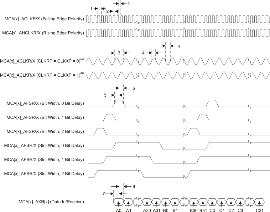
Table 9-80 Switching Characteristics Over Recommended Operating Conditions for McASP(1)
(see Figure 9-75)| NO. | PARAMETER | MIN | MAX | UNIT | ||
|---|---|---|---|---|---|---|
| 9 | tc(AHCLKRX) | Cycle time, MCA[x]_AHCLKR/X | 20(2) | ns | ||
| 10 | tw(AHCLKRX) | Pulse duration, MCA[x]_AHCLKR/X high or low | 0.5P - 2.5(3) | ns | ||
| 11 | tc(ACLKRX) | Cycle time, MCA[x]_ACLKR or ACLKX | 20 | ns | ||
| 12 | tw(ACLKRX) | Pulse duration, MCA[x]_ACLKR or ACLKX high or low | 0.5P - 2.5(3) | ns | ||
| 13 | td(ACLKRX-AFSRX) | Delay time, MCA[x]_ACLKR or ACLKX transmit edge to MCA[x]_AFSR/X output valid | ACLKR or ACLKX int | 0 | 6 | ns |
| ACLKR or ACLKX ext in | 2 | 13.5 | ||||
| Delay time, MCA[x]_ACLKR or ACLKX transmit edge to MCA[x]_AFSR/X output valid with Pad Loopback | ACLKR or ACLKX ext out | 2 | 13.5 | |||
| 14 | td(ACLKX-AXR) | Delay time, MCA[x]_ACLKX transmit edge to MCA[x]_AXR output valid | ACLKX int | -1 | 5 | ns |
| ACLKX ext in | 2 | 13.5 | ||||
| Delay time, MCA[x]_ACLKX transmit edge to MCA[x]_AXR output valid with Pad Loopback | ACLKX ext out | 2 | 13.5 | |||
| 15 | tdis(ACLKX-AXR) | Disable time, MCA[x]_ACLKX transmit edge to MCA[x]_AXR output high impedance | ACLKX int | -1 | 5 | ns |
| ACLKX ext in | 2 | 13.5 | ||||
| Disable time, MCA[x]_ACLKX transmit edge to MCA[x]_AXR output high impedance with Pad Loopback | ACLKX ext out | 2 | 13.5 | |||
ACLKR external input: ACLKRCTL.CLKRM=0, PDIR.ACLKR=0
ACLKR external output: ACLKRCTL.CLKRM=0, PDIR.ACLKR=1
ACLKX internal: ACLKXCTL.CLKXM=1, PDIR.ACLKX = 1
ACLKX external input: ACLKXCTL.CLKXM=0, PDIR.ACLKX=0
ACLKX external output: ACLKXCTL.CLKXM=0, PDIR.ACLKX=1
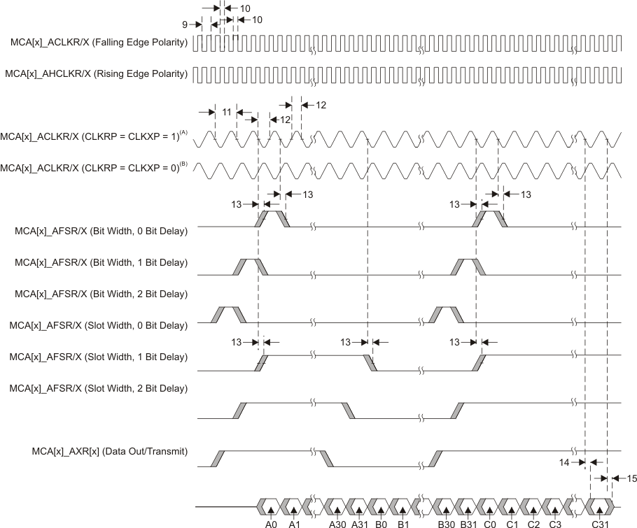
9.13 Multichannel Buffered Serial Port (McBSP)
The McBSP provides these functions:
- Full-duplex communication
- Double-buffered data registers, which allow a continuous data stream
- Independent framing and clocking for receive and transmit
- Direct interface to industry-standard codecs, analog interface chips (AICs), and other serially connected analog-to-digital (AD) and digital-to-analog (DA) devices
- Supports TDM, I2S, and similar formats
- External shift clock or an internal, programmable frequency shift clock for data transfer
- 5KB Tx and Rx buffer
- Supports three interrupt and two DMA requests.
The McBSP module may support two types of data transfer at the system level:
- The full-cycle mode, for which one clock period is used to transfer the data, generated on one edge and captured on the same edge (one clock period later).
- The half-cycle mode, for which one half clock period is used to transfer the data, generated on one edge and captured on the opposite edge (one half clock period later). Note that a new data is generated only every clock period, which secures the required hold time. The interface clock (CLKX or CLKR) activation edge (data or frame sync capture and generation) has to be configured accordingly with the external peripheral (activation edge capability) and the type of data transfer required at the system level.
For more detailed information on the McBSP peripheral, see the McBSP chapter in the TMS320DM816x DaVinci Digital Media Processors Technical Reference Manual (literature number SPRUGX8).
The following sections describe the timing characteristics for applications in normal mode (that is, the McBSP connected to one peripheral) and TDM applications in multipoint mode.
9.13.1 McBSP Peripheral Registers
This McBSP peripheral registers are described in the TMS320DM816x DaVinci Digital Media Processors Technical Reference Manual (literature number SPRUGX8). Each register is documented as an offset from a base address for the peripheral. The base addresses for all of the peripherals are shown in Table 3-26, L3 Memory Map.
9.13.2 McBSP Electrical Data and Timing
Table 9-81 Timing Requirements for McBSP - Master Mode(1)
(see Figure 9-76)| NO. | MIN | MAX | UNIT | ||
|---|---|---|---|---|---|
| 6 | tsu(DRV-CLKAE) | Setup time, MCB_DR valid before MCB_CLK active edge(2) | 3.5 | ns | |
| 7 | th(CLKAE-DRV) | Hold time, MCB_DR valid after MCB_CLK active edge(2) | 0.1 | ns | |
Table 9-82 Switching Characteristics Over Recommended Operating Conditions for McBSP - Master Mode(1)
(see Figure 9-76)| NO. | PARAMETER | MIN | MAX | UNIT | |
|---|---|---|---|---|---|
| 1 | tc(CLK) | Cycle time, output MCB_CLK period(2) | 20.83 | ns | |
| 2 | tw(CLKL) | Pulse duration, output MCB_CLK low(2) | 0.5*P - 1(3) | ns | |
| 3 | tw(CLKH) | Pulse duration, output MCB_CLK high(2) | 0.5*P - 1(3) | ns | |
| 4 | td(CLKAE-FSV) | Delay time, output MCB_CLK active edge to output MCB_FS valid(2)(4) | 0.7 | 9.4 | ns |
| 5 | td(CLKXAE-DXV) | Delay time, output MCB_CLKX active edge to output MCB_DX valid | 0.7 | 9.4 | ns |

McBSP in 6-pin mode: DX and DR as data pins; CLKX, CLKR, FSX and FSR as control pins.
McBSP in 4-pin mode: DX and DR as data pins; CLKX and FSX pins as control pins. The CLKX and FSX pins are internally looped back via software configuration, respectively to the CLKR and FSR internal signals for data receive.
Table 9-83 Timing Requirements for McBSP - Slave Mode(1)
(see Figure 9-77)| NO. | MIN | MAX | UNIT | ||
|---|---|---|---|---|---|
| 1 | tc(CLK) | Cycle time, MCB_CLK period(2) | 20.83 | ns | |
| 2 | tw(CLKL) | Pulse duration, MCB_CLK low(2) | 0.5*P - 1(3) | ns | |
| 3 | tw(CLKH) | Pulse duration, MCB_CLK high(2) | 0.5*P - 1(3) | ns | |
| 4 | tsu(FSV-CLKAE) | Setup time, MCB_FS valid before MCB_CLK active edge(2)(4) | 3.8 | ns | |
| 5 | th(CLKAE-FSV) | Hold time, MCB_FS valid after MCB_CLK active edge(2)(4) | 0 | ns | |
| 7 | tsu(DRV-CLKAE) | Setup time, MCB_DR valid before MCB_CLK active edge(2) | 3.8 | ns | |
| 8 | th(CLKAE-DRV) | Hold time, MCB_DR valid after MCB_CLK active edge(2) | 0 | ns | |
Table 9-84 Switching Characteristics Over Recommended Operating Conditions for McBSP - Slave Mode(1)
(see Figure 9-77)| NO. | PARAMETER | MIN | MAX | UNIT | |
|---|---|---|---|---|---|
| 6 | td(CLKXAE-DXV) | Delay time, input MCB_CLKx active edge to output MCB_DX valid | 0.5 | 12.5 | ns |

McBSP in 6-pin mode: DX and DR as data pins; CLKX, CLKR, FSX and FSR as control pins.
McBSP in 4-pin mode: DX and DR as data pins; CLKX and FSX pins as control pins. The CLKX and FSX pins are internally looped back via software configuration, respectively to the CLKR and FSR internal signals for data receive.
9.14 Peripheral Component Interconnect Express (PCIe)
The device supports connections to PCIe-compliant devices via the integrated PCIe master or slave bus interface. The PCIe module is comprised of a dual-mode PCIe core and a SerDes PHY. The device implements a single two-lane PCIe 2.0 (5.0 GT/s) endpoint or root complex port.
The device PCIe supports the following features:
- Supports Gen1 and Gen2 in x1 or x2 mode
- One port with up to 2 x 5 GT/s lanes
- Single virtual channel (VC), single traffic class (TC)
- Single function in end-point mode
- Automatic width and speed negotiation and lane reversal
- Max payload: 128 byte outbound, 256 byte inbound
- Automatic credit management
- ECRC generation and checking
- Configurable BAR filtering
- Supports PCIe messages
- Legacy interrupt reception (RC) and generation (EP)
- MSI generation and reception
- PCI device power management, except D3 cold with vaux
- Active state power management state L0 and L1.
For more detailed information on the PCIe port peripheral module, see the PCIe chapter in the TMS320DM816x DaVinci Digital Media Processors Technical Reference Manual (literature number SPRUGX8).
The PCIe peripheral on the device conforms to the PCI Express Base 2.0 Specification.
9.14.1 PCIe Design and Layout Specifications
NOTE
For more information on PCB layout, see the DM816xx Easy CYG Package PCB Escape Routing application report (literature number SPRABK6).
9.14.1.1 Clock Source
A standard 100-MHz PCIe differential clock source must be used for PCIe operation (for details, see Section 8.3.2).
9.14.1.2 PCIe Connections and Interface Compliance
The PCIe interface on the device is compliant with the PCI Express Base 2.0 Specification. Refer to the PCIe specifications for all connections that are described in it. For coupling capacitor selection, see Section 9.14.1.2.1.
The use of PCIe-compatible bridges and switches is allowed for interfacing with more than one other processor or PCIe device.
9.14.1.2.1 Coupling Capacitors
AC coupling capacitors are required on the transmit data pair. Table 9-85 shows the requirements for these capacitors.
Table 9-85 AC Coupling Capacitors Requirements
| PARAMETER | MIN | TYP | MAX | UNIT |
|---|---|---|---|---|
| PCIe AC coupling capacitor value | 75 | 200 | nF | |
| PCIe AC coupling capacitor package size(1) | 0402 | 0603 | EIA(2) |
9.14.1.2.2 Polarity Inversion
The PCIe specification requires polarity inversion support. This means, for layout purposes, polarity is unimportant since each signal can change its polarity on-die inside the chip. This means polarity within a lane is unimportant for layout.
9.14.1.2.3 Lane Reversal
The device supports lane reversal. Since there are two lanes, this means the lanes can be switched in layout for better PCB routing.
9.14.1.3 Non-Standard PCIe Connections
The following sections contain suggestions for any PCIe connection that is not described in the official PCIe specification, such as an on-board device-to-device connection, or device-to-other PCIe-compliant processor connection.
9.14.1.3.1 PCB Stackup Specifications
Table 9-86 shows the stackup and feature sizes required for these types of PCIe connections.
Table 9-86 PCIe PCB Stackup Specifications
| PARAMETER | MIN | TYP | MAX | UNIT |
|---|---|---|---|---|
| PCB Routing and Plane Layers | 4 | 6 | - | Layers |
| Signal Routing Layers | 2 | 3 | - | Layers |
| Number of ground plane cuts allowed within PCIe routing region | - | - | 0 | Cuts |
| Number of layers between PCIe routing area and reference plane(1) | - | - | 0 | Layers |
| PCB Routing clearance | - | 4 | - | Mils |
| PCB Trace width(2) | - | 4 | - | Mils |
| PCB BGA escape via pad size | - | 20 | - | Mils |
| PCB BGA escape via hole size | - | 10 | Mils | |
| Processor BGA pad size(3)(4) | 0.3 | mm |
9.14.1.3.2 Routing Specifications
The PCIe data signal traces must be routed to achieve 100 Ω (±20%) differential impedance and 60 Ω (±15%) single-ended impedance. The single-ended impedance is required because differential signals are extremely difficult to closely couple on PCBs and, therefore, single-ended impedance becomes important. These requirements are the same as those recommended in the PCIe Motherboard Checklist 1.0 document, available from PCI-SIG.
These impedances are impacted by trace width, trace spacing, distance between signals and referencing planes, and dielectric material. Verify with a PCB design tool that the trace geometry for both data signal pairs result in as close to 100 Ω differential impedance and 60 Ω single-ended impedance as possible. For best accuracy, work with your PCB fabricator to ensure this impedance is met.
In general, closely coupled differential signal traces are not an advantage on PCBs. When differential signals are closely coupled, tight spacing and width control is necessary. Very small width and spacing variations affect impedance dramatically, so tight impedance control can be more problematic to maintain in production.
Loosely coupled PCB differential signals make impedance control much easier. Wider traces and spacing make obstacle avoidance easier, and trace width variations do not affect impedance as much; therefore, it is easier to maintain an accurate impedance over the length of the signal. The wider traces also show reduced skin effect and, therefore, often result in better signal integrity.
Table 9-87 shows the routing specifications for the PCIe data signals.
Table 9-87 PCIe Routing Specifications
| PARAMETER | MIN | TYP | MAX | UNIT |
|---|---|---|---|---|
| PCIe signal trace length | 10(1) | Inches | ||
| Differential pair trace matching | 10(2) | Mils | ||
| Number of stubs allowed on PCIe traces(3) | 0 | Stubs | ||
| TX or RX pair differential impedance | 80 | 100 | 120 | Ω |
| TX or RX single-ended impedance | 51 | 60 | 69 | Ω |
| Pad size of vias on PCIe trace | 25(4) | Mils | ||
| Hole size of vias on PCIe trace | 14 | Mils | ||
| Number of vias on each PCIe trace | 3 | Vias(5) | ||
| PCIe differential pair to any other trace spacing | 2*DS(6) |
9.14.2 PCIe Peripheral Register Descriptions
Table 9-88 PCIe Registers
| HEX ADDRESS | ACRONYM | REGISTER NAME |
|---|---|---|
| 0x5100 0000 | PID | Peripheral Version and ID |
| 0x5100 0004 | CMD_STATUS | Command Status |
| 0x5100 0008 | CFG_SETUP | Config Transaction Setup |
| 0x5100 000C | IOBASE | IO TLP Base |
| 0x5100 0010 | TLPCFG | TLP Attribute Configuration |
| 0x5100 0014 | RSTCMD | Reset Command and Status |
| 0x5100 0020 | PMCMD | Power Management Command |
| 0x5100 0024 | PMCFG | Power Management Configuration |
| 0x5100 0028 | ACT_STATUS | Activity Status |
| 0x5100 0030 | OB_SIZE | Outbound Size |
| 0x5100 0034 | DIAG_CTRL | Diagnostic Control |
| 0x5100 0038 | ENDIAN | Endian Mode |
| 0x5100 003C | PRIORITY | CBA Transaction Priority |
| 0x5100 0050 | IRQ_EOI | End of Interrupt |
| 0x5100 0054 | MSI_IRQ | MSI Interrupt IRQ |
| 0x5100 0064 | EP_IRQ_SET | Endpoint Interrupt Request Set |
| 0x5100 0068 | EP_IRQ_CLR | Endpoint Interrupt Request Clear |
| 0x5100 006C | EP_IRQ_STATUS | Endpoint Interrupt Status |
| 0x5100 0070 | GPRO | General Purpose 0 |
| 0x5100 0074 | GPR1 | General Purpose 1 |
| 0x5100 0078 | GPR2 | General Purpose 2 |
| 0x5100 007C | GPR3 | General Purpose 3 |
| 0x5100 0100 | MSI0_IRQ_STATUS_RAW | MSI 0 Interrupt Raw Status |
| 0x5100 0104 | MSI0_IRQ_STATUS | MSI 0 Interrupt Enabled Status |
| 0x5100 0108 | MSI0_IRQ_ENABLE_SET | MSI 0 Interrupt Enable Set |
| 0x5100 010C | MSI0_IRQ_ENABLE_CLR | MSI 0 Interrupt Enable Clear |
| 0x5100 0180 | IRQ_STATUS_RAW | Raw Interrupt Status |
| 0x5100 0184 | IRQ_STATUS | Interrupt Enabled Status |
| 0x5100 0188 | IRQ_ENABLE_SET | Interrupt Enable Set |
| 0x5100 018C | IRQ_ENABLE_CLR | Interrupt Enable Clear |
| 0x5100 01C0 | ERR_IRQ_STATUS_RAW | Raw ERR Interrupt Status |
| 0x5100 01C4 | ERR_IRQ_STATUS | ERR Interrupt Enabled Status |
| 0x5100 01C8 | ERR_IRQ_ENABLE_SET | ERR Interrupt Enable Set |
| 0x5100 01CC | ERR_IRQ_ENABLE_CLR | ERR Interrupt Enable Clear |
| 0x5100 01D0 | PMRST_IRQ_STATUS_RAW | Power Management and Reset Interrupt Status |
| 0x5100 01D4 | PMRST_IRQ_STATUS | Power Management and Reset Interrupt Enabled Status |
| 0x5100 01D8 | PMRST_ENABLE_SET | Power Management and Reset Interrupt Enable Set |
| 0x5100 01DC | PMRST_ENABLE_CLR | Power Management and Reset Interrupt Enable Clear |
| 0x5100 0200 | OB_OFFSET_INDEXn | Outbound Translation Region N Offset Low and Index |
| 0x5100 0204 | OB_OFFSETn_HI | Outbound Translation Region N Offset High |
| 0x5100 0300 | IB_BAR0 | Inbound Translation Bar Match 0 |
| 0x5100 0304 | IB_START0_LO | Inbound Translation 0 Start Address Low |
| 0x5100 0308 | IB_START0_HI | Inbound Translation 0 Start Address High |
| 0x5100 030C | IB_OFFSET0 | Inbound Translation 0 Address Offset |
| 0x5100 0310 | IB_BAR1 | Inbound Translation Bar Match 1 |
| 0x5100 0314 | IB_START1_LO | Inbound Translation 1 Start Address Low |
| 0x5100 0318 | IB_START1_HI | Inbound Translation 1 Start Address High |
| 0x5100 031C | IB_OFFSET1 | Inbound Translation 1 Address Offset |
| 0x5100 0320 | IB_BAR2 | Inbound Translation Bar Match 2 |
| 0x5100 0324 | IB_START2_LO | Inbound Translation 2 Start Address Low |
| 0x5100 0328 | IB_START2_HI | Inbound Translation 2 Start Address High |
| 0x5100 032C | IB_OFFSET2 | Inbound Translation 2 Address Offset |
| 0x5100 0330 | IB_BAR3 | Inbound Translation Bar Match 3 |
| 0x5100 0334 | IB_START3_LO | Inbound Translation 3 Start Address Low |
| 0x5100 0338 | IB_START3_HI | Inbound Translation 3 Start Address High |
| 0x5100 033C | IB_OFFSET3 | Inbound Translation 3 Address Offset |
| 0x5100 0380 | PCS_CFG0 | PCS Configuration 0 |
| 0x5100 0384 | PCS_CFG1 | PCS Configuration 1 |
| 0x5100 0388 | PCS_STATUS | PCS Status |
| 0x5100 0390 | SERDES_CFG0 | SerDes Configuration for Lane 0 |
| 0x5100 0394 | SERDES_CFG1 | SerDes Configuration for Lane 1 |
9.14.3 PCIe Electrical Data and Timing
Texas Instruments (TI) has performed the simulation and system characterization to ensure that the PCIe peripheral meets all AC timing specifications as required by the PCI Express Base 2.0 Specification. Therefore, the AC timing specifications are not reproduced here. For more information on the AC timing specifications, see Sections 4.3.3.5 and 4.3.4.4 of the PCI Express Base 2.0 Specification.
9.15 Real-Time Clock (RTC)
The real-time clock is a precise timer that can generate interrupts on intervals specified by the user. Interrupts can occur every second, minute, hour, or day. The clock, itself, can track the passage of real time for durations of several years, provided it has a sufficient power source the whole time.
The basic purpose for the RTC is to keep time of day. The other equally important purpose of the RTC is for Digital Rights management. Some degree of tamper-proofing is needed to ensure that simply stopping, resetting, or corrupting the RTC does not go unnoticed; so, if this occurs, the application can re-acquire the time of day from a trusted source. The final purpose of RTC is to wake up the rest of the device from a power-down state. The RTC features include:
- Time information (hours, minutes, seconds) directly in binary coded decimal (BCD), for easy decoding.
- Calendar information (day, month, year, day of week) directly in BCD code up to year 2099.
- Shadow time and calendar access; ease of reading time.
- Interrupt generation, periodically (1d, 1h, 1m, 1s) or at a precise time of day or date.
- 30-second time correction (crystal frequency compensation).
- OCP slave port for register access.
- Supports power idle protocol with SWakeUp capable on alarm or timer events.
The RTC is driven by SYSCLK18 (32.768 kHz) or an optional 32.768-kHz clock can be input on the CLKIN32 clock input pin for RTC reference. If the CLKIN32 pin is not connected to a 32.768-kHz clock input, this pin should be pulled low.
Figure 9-78 shows the major components of the RTC.
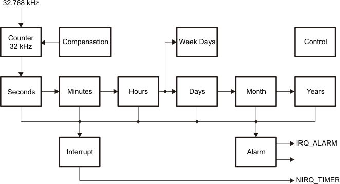 Figure 9-78 Real-Time Clock Block Diagram
9.15.1 RTC Register Descriptions
Table 9-89 RTC Registers
| HEX ADDRESS | ACRONYM | REGISTER NAME |
|---|---|---|
| 0x480C 0000 | SECONDS_REG | Seconds |
| 0x480C 0004 | MINUTES_REG | Minutes |
| 0x480C 0008 | HOURS_REG | Hours |
| 0x480C 000C | DAYS_REG | Day of the Month |
| 0x480C 0010 | MONTHS_REG | Month |
| 0x480C 0014 | YEARS_REG | Year |
| 0x480C 0018 | WEEK_REG | Day of the Week |
| 0x480C 0020 | ALARM_SECONDS_REG | Alarm Seconds |
| 0x480C 0024 | ALARM_MINUTES_REG | Alarm Minutes |
| 0x480C 0028 | ALARM_HOURS_REG | Alarm Hours |
| 0x480C 002C | ALARM_DAYS_REG | Alarm Days |
| 0x480C 0030 | ALARM_MONTHS_REG | Alarm Months |
| 0x480C 0034 | ALARM_YEARS_REG | Alarm Years |
| 0x480C 0040 | RTC_CTRL_REG | Control |
| 0x480C 0044 | RTC_STATUS_REG | Status |
| 0x480C 0048 | RTC_INTERRUPTS_REG | Interrupt Enable |
| 0x480C 004C | RTC_COMP_LSB_REG | Compensation (LSB) |
| 0x480C 0050 | RTC_COMP_MSB_REG | Compensation (MSB) |
| 0x480C 0054 | RTC_OSC_REG | Oscillator |
| 0x480C 0060 | RTC_SCRATCH0_REG | Scratch 0 (general-purpose) |
| 0x480C 0064 | RTC_SCRATCH1_REG | Scratch 1 (general-purpose) |
| 0x480C 0068 | RTC_SCRATCH2_REG | Scratch 2 (general-purpose) |
| 0x480C 006C | KICK0 | Kick 0 (write protect) |
| 0x480C 0070 | KICK1 | Kick 1 (write protect) |
| 0x480C 0074 | RTC_REVISION | Revision |
| 0x480C 0078 | RTC_SYSCONFIG | Clock Management Configuration |
| 0x480C 007A | RTC_IRQWAKEEN_0 | Wakeup Generation |
9.16 Secure Digital and Secure Digital Input Output (SD and SDIO)
The device SD and SDIO Controller has following features:
- Secure Digital (SD) memory card with Secure Data IO (SDIO)
- Supports SDHC (SD high capacity)
- SD and SDIO protocol support
- Programmable clock frequency
- 1024 byte read or write FIFO to lower system overhead
- Slave DMA transfer capability
- Full compliance with SD command and response sets, as defined in the SD physical layer specification v2.00
- Full compliance with SDIO command and response sets and interrupt and read-wait suspend-resume operations, as defined in the SD part E1 specification v 2.00
- Full compliance with SD host controller standard specification sets as defined in the SD card specification part A2 v2.00.
For more detailed information on SD and SDIO, see the SD and SDIO chapter in the TMS320DM816x DaVinci Digital Media Processors Technical Reference Manual (literature number SPRUGX8).
9.16.1 SD and SDIO Peripheral Register Descriptions
Table 9-90 SD and SDIO Registers(1)
| HEX ADDRESS | ACRONYM | REGISTER NAME |
|---|---|---|
| 0x4806 0000 | SD_HL_REV | IP Revision Identifier |
| 0x4806 0004 | SD_HL_HWINFO | Hardware Configuration |
| 0x4806 0010 | SD_HL_SYSCONFIG | Clock Management Configuration |
| 0x4806 0110 | SD_SYSCONFIG | System Configuration |
| 0x4806 0114 | SD_SYSSTATUS | System Status |
| 0x4806 0124 | SD_CSRE | Card status response error |
| 0x4806 0128 | SD_SYSTEST | System Test |
| 0x4806 012C | SD_CON | Configuration |
| 0x4806 0130 | SD_PWCNT | Power counter |
| 0x4806 0200 | SD_SDMASA | SDMA System address: |
| 0x4806 0204 | SD_BLK | Transfer Length Configuration |
| 0x4806 0208 | SD_ARG | Command argument |
| 0x4806 020C | SD_CMD | Command and transfer mode |
| 0x4806 0210 | SD_RSP10 | Command Response 0 and 1 |
| 0x4806 0214 | SD_RSP32 | Command Response 2 and 3 |
| 0x4806 0218 | SD_RSP54 | Command Response 4 and 5 |
| 0x4806 021C | SD_RSP76 | Command Response 6 and 7 |
| 0x4806 0220 | SD_DATA | Data |
| 0x4806 0224 | SD_PSTATE | Present state |
| 0x4806 0228 | SD_HCTL | Host Control |
| 0x4806 022C | SD_SYSCTL | SD system control |
| 0x4806 0230 | SD_STAT | Interrupt status |
| 0x4806 0234 | SD_IE | Interrupt SD enable |
| 0x4806 0238 | SD_ISE | |
| 0x4806 023C | SD_AC12 | Auto CMD12 Error Status |
| 0x4806 0240 | SD_CAPA | Capabilities |
| 0x4806 0248 | SD_CUR_CAPA | Maximum current capabilities |
| 0x4806 0250 | SD_FE | Force Event |
| 0x4806 0254 | SD_ADMAES | ADMA Error Status |
| 0x4806 0258 | SD_ADMASAL | ADMA System address Low bits |
| 0x4806 025C | SD_ADMASAH | ADMA System address High bits |
| 0x4806 02FC | SD_REV | Versions |
9.16.2 SD and SDIO Electrical Data and Timing
9.16.2.1 SD Identification and Standard SD Mode
Table 9-91 Timing Requirements for SD and SDIO—SD Identification and Standard SD Mode
(see Figure 9-80, Figure 9-82)Table 9-92 Switching Characteristics Over Recommended Operating Conditions for SD and SDIO—SD Identification and Standard SD Mode
(see Figure 9-79, Figure 9-80, Figure 9-81, Figure 9-82)| NO. | PARAMETER | MIN | MAX | UNIT | |
|---|---|---|---|---|---|
| SD Identification Mode | |||||
| 8 | fop(CLKID) | Identification mode frequency, SD_CLK | 400 | kHz | |
| tc(CLKID) | Identification mode period, SD_CLK | 2500.0 | ns | ||
| 13 | td(CLKH-CMD) | Delay time, SD_CLK rising clock edge to SD_CMD transition | 6.5 | 2492.5 | ns |
| Standard SD Mode | |||||
| 7 | fop(CLK) | Operating frequency, SD_CLK | 24 | MHz | |
| tc(CLK) | Operating period, SD_CLK | 41.7 | ns | ||
| 9 | tw(CLKL) | Pulse duration, SD_CLK low | 0.45*P(1) | 0.55*P(1) | ns |
| 10 | tw(CLKH) | Pulse duration, SD_CLK high | 0.45*P(1) | 0.55*P(1) | ns |
| 13 | td(CLKH-CMD) | Delay time, SD_CLK rising clock edge to SD_CMD transition | 6.3 | 35.3 | ns |
| 14 | td(CLKH-DAT) | Delay time, SD_CLK rising clock edge to SD_DATx transition | 6.3 | 35.3 | ns |
9.16.2.2 High-Speed SD Mode
Table 9-93 Timing Requirements for SD and SDIO—High-Speed SD Mode
(see Figure 9-80, Figure 9-82)| NO. | MIN | MAX | UNIT | ||
|---|---|---|---|---|---|
| 1 | tsu(CMDV-CLKH) | Setup time, SD_CMD valid before SD_CLK rising clock edge | 4.1 | ns | |
| 2 | th(CLKH-CMDV) | Hold time, SD_CMD valid after SD_CLK rising clock edge | 1.9 | ns | |
| 3 | tsu(DATV-CLKH) | Setup time, SD_DATx valid before SD_CLK rising clock edge | 4.1 | ns | |
| 4 | th(CLKH-DATV) | Hold time, SD_DATx valid after SD_CLK rising clock edge | 1.9 | ns | |
Table 9-94 Switching Characteristics Over Recommended Operating Conditions for SD and SDIO—High-Speed SD Mode
(see Figure 9-79, Figure 9-80, Figure 9-81, Figure 9-82)| NO. | PARAMETER | MIN | MAX | UNIT | |
|---|---|---|---|---|---|
| 7 | fop(CLK) | Operating frequency, SD_CLK | 48 | MHz | |
| tc(CLK) | Operating period: SD_CLK | 20.8 | ns | ||
| 8 | fop(CLKID) | Identification mode frequency, SD_CLK | 400 | kHz | |
| tc(CLKID) | Identification mode period: SD_CLK | 2500.0 | ns | ||
| 9 | tw(CLKL) | Pulse duration, SD_CLK low | 0.5*P(1) | ns | |
| 10 | tw(CLKH) | Pulse duration, SD_CLK high | 0.5*P(1) | ns | |
| 11 | tr(CLK) | Rise time, All Signals (10% to 90%) | 2.2 | ns | |
| 12 | tf(CLK) | Fall time, All Signals (10% to 90%) | 2.2 | ns | |
| 13 | td(CLKL-CMD) | Delay time, SD_CLK rising clock edge to SD_CMD transition | 2.5(2) | 13.9 | ns |
| 14 | td(CLKL-DAT) | Delay time, SD_CLK rising clock edge to SD_DATx transition | 2.5(2) | 13.9 | ns |
 Figure 9-79 SD Host Command Timing
 Figure 9-80 SD Card Response Timing
 Figure 9-81 SD Host Write Timing
 Figure 9-82 SD Host Read and Card CRC Status Timing
9.17 Serial ATA Controller (SATA)
The Serial ATA (SATA) peripheral provides a direct interface for up to two hard disk drives (SATA) and supports the following features:
- Serial ATA 1.5 Gbps and 3 Gbps speeds
- Integrated PHY
- Integrated Rx and Tx data buffers
- Supports all SATA power management features
- Hardware-assisted native command queuing (NCQ) for up to 32 entries
- Supports port multiplier with command-based switching for connection to multiple hard disk drives
- Activity LED support.
For more detailed information on the SATA, see the SATA chapter in the TMS320DM816x DaVinci Digital Media Processors Technical Reference Manual (literature number SPRUGX8).
9.17.1 SATA Interface Design Specifications
NOTE
For more information on PCB layout, see the DM816xx Easy CYG Package PCB Escape Routing application report (literature number SPRABK6).
This section provides PCB design and layout specifications for the SATA interface. The design rules constrain PCB trace length, PCB trace skew, signal integrity, cross-talk, and signal timing. Simulation and system design work has been done to ensure the SATA interface requirements are met.
A standard 100-MHz differential clock source must be used for SATA operation (for details, see Section 8.3.2).
9.17.1.1 SATA Interface Schematic
Figure 9-83 shows the data portion of the SATA interface schematic. The specific pin numbers can be obtained from Table 4-17, Serial ATA Terminal Functions.
 Figure 9-83 SATA Interface High-Level Schematic
9.17.1.2 Compatible SATA Components and Modes
Table 9-95 shows the compatible SATA components and supported modes. Note that the only supported configuration is an internal cable from the processor host to the SATA device.
Table 9-95 SATA Supported Modes
| PARAMETER | MIN | MAX | UNIT | SUPPORTED |
|---|---|---|---|---|
| Transfer Rates | 1.5 | 3.0 | Gbps | |
| eSATA | - | - | - | No |
| xSATA | - | - | - | No |
| Backplane | - | - | - | No |
| Internal Cable | - | - | - | Yes |
9.17.1.3 PCB Stackup Specifications
Table 9-96 shows the PCB stackup and feature sizes required for SATA.
Table 9-96 SATA PCB Stackup Specifications
| PARAMETER | MIN | TYP | MAX | UNIT |
|---|---|---|---|---|
| PCB routing and plane layers | 4 | 6 | - | Layers |
| Signal routing layers | 2 | 3 | - | Layers |
| Number of ground plane cuts allowed within SATA routing region | - | - | 0 | Cuts |
| Number of layers between SATA routing region and reference ground plane | - | - | 0 | Layers |
| PCB trace width, w | - | 4 | - | Mils |
| PCB BGA escape via pad size | - | 20 | - | Mils |
| PCB BGA escape via hole size | - | 10 | Mils | |
| Processor BGA pad size(1) | 0.3 | mm |
9.17.1.4 Routing Specifications
The SATA data signal traces must be routed to achieve 100 Ω (±20%) differential impedance and 60 Ω (±15%) single-ended impedance. The single-ended impedance is required because differential signals are extremely difficult to closely couple on PCBs and, therefore, single-ended impedance becomes important. 60 Ω is chosen for the single-ended impedance to minimize problems caused by too low an impedance.
These impedances are impacted by trace width, trace spacing, distance to reference planes, and dielectric material. Verify with a PCB design tool that the trace geometry for both data signal pairs results in as close to 100 Ω differential impedance and 60 Ω single-ended impedance traces as possible. For best accuracy, work with your PCB fabricator to ensure this impedance is met.
Table 9-97 shows the routing specifications for the SATA data signals.
Table 9-97 SATA Routing Specifications
| PARAMETER | MIN | TYP | MAX | UNIT |
|---|---|---|---|---|
| Processor-to-SATA header trace length | 10(1) | Inches | ||
| Number of stubs allowed on SATA traces(2) | 0 | Stubs | ||
| TX and RX pair differential impedance | 80 | 100 | 120 | Ω |
| TX and RX single-ended impedance | 51 | 60 | 69 | Ω |
| Number of vias on each SATA trace | 3 | Vias(3) | ||
| SATA differential pair to any other trace spacing | 2*DS(4) |
9.17.1.5 Coupling Capacitors
AC coupling capacitors are required on the receive data pair. Table 9-98 shows the requirements for these capacitors.
Table 9-98 SATA AC Coupling Capacitors Requirements
| PARAMETER | MIN | TYP | MAX | UNIT |
|---|---|---|---|---|
| SATA AC coupling capacitor value | 1 | 10 | 12 | nF |
| SATA AC coupling capacitor package size(1) | 0402 | 0603 | EIA(2) |
9.17.2 SATA Peripheral Register Descriptions
Table 9-99 SATA Registers
| HEX ADDRESS | ACRONYM | REGISTER NAME |
|---|---|---|
| 0x4A14 0000 | CAP | HBA Capabilities |
| 0x4A14 0004 | GHC | Global HBA Control |
| 0x4A14 0008 | IS | Interrupt Status |
| 0x4A14 000C | PI | Ports Implemented |
| 0x4A14 0010 | VS | AHCI Version |
| 0x4A14 0014 | CCC_CTL | Command Completion Coalescing Control |
| 0x4A14 0018 | CCC_PORTS | Command Completion Coalescing Ports |
| 0x4A14 001C - 0x4A14 009C | - | Reserved |
| 0x4A14 00A0 | BISTAFR | BIST Active FIS |
| 0x4A14 00A4 | BISTCR | BIST Control |
| 0x4A14 00A8 | BISTFCTR | BIST FIS Count |
| 0x4A14 00AC | BISTSR | BIST Status |
| 0x4A14 00B0 | BISTDECR | BIST DWORD Error Count |
| 0x4A14 00B4 - 0x4A14 00DF | - | Reserved |
| 0x4A14 00E0 | TIMER1MS | BIST DWORD Error Count |
| 0x4A14 00E4 | - | Reserved |
| 0x4A14 00E8 | GPARAM1R | Global Parameter 1 |
| 0x4A14 00EC | GPARAM2R | Global Parameter 2 |
| 0x4A14 00F0 | PPARAMR | Port Parameter |
| 0x4A14 00F4 | TESTR | Test |
| 0x4A14 00F8 | VERSIONR | Version |
| 0x4A14 00FC | IDR (PID) | ID |
| 0x4A14 0100 | P0CLB | Port 0 Command List Base Address |
| 0x4A14 0104 | - | Reserved |
| 0x4A14 0108 | P0FB | Port 0 FIS Base Address |
| 0x4A14 010C | - | Reserved |
| 0x4A14 0110 | P0IS | Port 0 Interrupt Status |
| 0x4A14 0114 | P0IE | Port 0 Interrupt Enable |
| 0x4A14 0118 | P0CMD | Port 0 Command |
| 0x4A14 011C | - | Reserved |
| 0x4A14 0120 | P0TFD | Port 0 Task File Data |
| 0x4A14 0124 | P0SIG | Port 0 Signature |
| 0x4A14 0128 | P0SSTS | Port 0 Serial ATA Status (SStatus) |
| 0x4A14 012C | P0SCTL | Port 0 Serial ATA Control (SControl) |
| 0x4A14 0130 | P0SERR | Port 0 Serial ATA Error (SError) |
| 0x4A14 0134 | P0SACT | Port 0 Serial ATA Active (SActive) |
| 0x4A14 0138 | P0CI | Port 0 Command Issue |
| 0x4A14 013C | P0SNTF | Port 0 Serial ATA Notification |
| 0x4A14 0140 - 0x4A14 016C | - | Reserved |
| 0x4A14 0170 | P0DMACR | Port 0 DMA Control |
| 0x4A14 0174 | - | Reserved |
| 0x4A14 0178 | P0PHYCR | Port 0 PHY Control |
| 0x4A14 017C | P0PHYSR | Port 0 PHY Status |
| 0x4A14 0180 | P1CLB | Port 1 Command List Base Address |
| 0x4A14 0184 | - | Reserved |
| 0x4A14 0188 | P1FB | Port 1 FIS Base Address |
| 0x4A14 018C | - | Reserved |
| 0x4A14 0190 | P1IS | Port 1 Interrupt Status |
| 0x4A14 0194 | P1IE | Port 1 Interrupt Enable |
| 0x4A14 0198 | P1CMD | Port 1 Command |
| 0x4A14 019C | - | Reserved |
| 0x4A14 01A0 | P1TFD | Port 1 Task File Data |
| 0x4A14 01A4 | P1SIG | Port 1 Signature |
| 0x4A14 01A8 | P1SSTS | Port 1 Serial ATA Status (SStatus) |
| 0x4A14 01AC | P1SCTL | Port 1 Serial ATA Control (SControl) |
| 0x4A14 01B0 | P1SERR | Port 1 Serial ATA Error (SError) |
| 0x4A14 01B4 | P1SACT | Port 1 Serial ATA Active (SActive) |
| 0x4A14 01B8 | P1CI | Port 1 Command Issue |
| 0x4A14 01BC | P1SNTF | Port 1 Serial ATA Notification |
| 0x4A14 01C0 - 0x4A14 01EC | - | Reserved |
| 0x4A14 01F0 | P1DMACR | Port 1 DMA Control |
| 0x4A14 01F4 | - | Reserved |
| 0x4A14 01F8 | P1PHYCR | Port 1 PHY Control |
| 0x4A14 01FC | P1PHYSR | Port 1 PHY Status |
| 0x4A14 1100 | IDLE | Idle and Standby Modes |
| 0x4A14 1104 | PHYCFGR2 | PHY Configuration 2 |
9.18 Serial Peripheral Interface (SPI)
The SPI is a high-speed synchronous serial input and output port that allows a serial bit stream of programmed length (4 to 32 bits) to be shifted into and out of the device at a programmed bit-transfer rate. The SPI is normally used for communication between the device and external peripherals. Typical applications include an interface-to-external IO or peripheral expansion via devices such as shift registers, display drivers, SPI EEPROMs, and analog-to-digital converters (ADCs).
The SPI supports the following features:
- Master and slave operation
- Four chip selects for interfacing and control to up to four SPI slave devices and connection to a single external master
- 32-bit shift register
- Buffered receive and transmit data register per channel (1 word deep), FIFO size is 64 bytes
- Programmable SPI configuration per channel (clock definition, enable polarity and word width)
- Supports one interrupt request and two DMA requests per channel.
For more detailed information on the SPI, see the SPI chapter in the TMS320DM816x DaVinci Digital Media Processors Technical Reference Manual (literature number SPRUGX8).
9.18.1 SPI Peripheral Register Descriptions
Table 9-100 SPI Registers
| HEX ADDRESS | ACRONYM | REGISTER NAME |
|---|---|---|
| 0x4803 0000 - 0x4803 010C | - | RESERVED |
| 0x4803 0110 | MCSPI_SYSCONFIG | SYSTEM CONFIGURATION |
| 0x4803 0114 | MCSPI_SYSSTATUS | SYSTEM STATUS |
| 0x4803 0118 | MCSPI_IRQSTATUS | INTERRUPT STATUS |
| 0x4803 011C | MCSPI_IRQENABLE | INTERRUPT ENABLE |
| 0x4803 0120 | - | RESERVED |
| 0x4803 0124 | MCSPI_SYST | SYSTEM TEST |
| 0x4803 0128 | MCSPI_MODULCTRL | MODULE CONTROL |
| 0x4803 012C | MCSPI_CH0CONF | CHANNEL 0 CONFIGURATION |
| 0x4803 0130 | MCSPI_CH0STAT | CHANNEL 0 STATUS |
| 0x4803 0134 | MCSPI_CH0CTRL | CHANNEL 0 CONTROL |
| 0x4803 0138 | MCSPI_TX0 | CHANNEL 0 TRANSMITTER |
| 0x4803 013C | MCSPI_RX0 | CHANNEL 0 RECEIVER |
| 0x4803 0140 | MCSPI_CH1CONF | CHANNEL 1 CONFIGURATION |
| 0x4803 0144 | MCSPI_CH1STAT | CHANNEL 1 STATUS |
| 0x4803 0148 | MCSPI_CH1CTRL | CHANNEL 1 CONTROL |
| 0x4803 014C | MCSPI_TX1 | CHANNEL 1 TRANSMITTER |
| 0x4803 0150 | MCSPI_RX1 | CHANNEL 1 RECEIVER |
| 0x4803 0154 | MCSPI_CH2CONF | CHANNEL 2 CONFIGURATION |
| 0x4803 0158 | MCSPI_CH2STAT | CHANNEL 2 STATUS |
| 0x4803 015C | MCSPI_CH2CTRL | CHANNEL 2 CONTROL |
| 0x4803 0160 | MCSPI_TX2 | CHANNEL 2 TRANSMITTER |
| 0x4803 0164 | MCSPI_RX2 | CHANNEL 2 RECEIVER |
| 0x4803 0168 | MCSPI_CH3CONF | CHANNEL 3 CONFIGURATION |
| 0x4803 016C | MCSPI_CH3STAT | CHANNEL 3 STATUS |
| 0x4803 0170 | MCSPI_CH3CTRL | CHANNEL 3 CONTROL |
| 0x4803 0174 | MCSPI_TX3 | CHANNEL 3 TRANSMITTER |
| 0x4803 0178 | MCSPI_RX3 | CHANNEL 3 RECEIVER |
| 0x4803 017C | MCSPI_XFERLEVEL | TRANSFER LEVELS |
| 0x4803 0180 - 0x4803 01FF | - | RESERVED |
9.18.2 SPI Electrical Data and Timing
Table 9-101 Timing Requirements for SPI - Master Mode
(see Figure 9-84 and Figure 9-85)| NO. | MIN | MAX | UNIT | |||
|---|---|---|---|---|---|---|
| MASTER: 1 LOAD AT A MAXIMUM OF 5 pF | ||||||
| 1 | tc(SPICLK) | Cycle time, SPI_CLK(1)(2) | 20.8(3) | ns | ||
| 2 | tw(SPICLKL) | Pulse duration, SPI_CLK low(1) | 0.5*P - 1(4) | ns | ||
| 3 | tw(SPICLKH) | Pulse duration, SPI_CLK high(1) | 0.5*P - 1(4) | ns | ||
| 4 | tsu(MISO-SPICLK) | Setup time, SPI_D[x] valid before SPI_CLK active edge(1) | 2.29 | ns | ||
| 5 | th(SPICLK-MISO) | Hold time, SPI_D[x] valid after SPI_CLK active edge(1) | 2.67 | ns | ||
| 6 | td(SPICLK-MOSI) | Delay time, SPI_CLK active edge to SPI_D[x] transition(1) | -3.57 | 3.57 | ns | |
| 7 | td(SCS-MOSI) | Delay time, SPI_SCS[x] active edge to SPI_D[x] transition | 3.57 | ns | ||
| 8 | td(SCS-SPICLK) | Delay time, SPI_SCS[x] active to SPI_CLK first edge(1) | MASTER_PHA0(5) | B-4.2(6) | ns | |
| MASTER_PHA1(5) | A-4.2(7) | ns | ||||
| 9 | td(SPICLK-SCS) | Delay time, SPI_CLK last edge to SPI_SCS[x] inactive(1) | MASTER_PHA0(5) | A-4.2(7) | ns | |
| MASTER_PHA1(5) | B-4.2(6) | ns | ||||
| MASTER: UP TO 4 LOADS AT A MAXIMUM TOTAL OF 25 pF | ||||||
| 1 | tc(SPICLK) | Cycle time, SPI_CLK(1)(2) | 41.7(8) | ns | ||
| 2 | tw(SPICLKL) | Pulse duration, SPI_CLK low(1) | 0.5*P - 2(4) | ns | ||
| 3 | tw(SPICLKH) | Pulse duration, SPI_CLK high(1) | 0.5*P - 2(4) | ns | ||
| 4 | tsu(MISO-SPICLK) | Setup time, SPI_D[x] valid before SPI_CLK active edge(1) | 3.02 | ns | ||
| 5 | th(SPICLK-MISO) | Hold time, SPI_D[x] valid after SPI_CLK active edge(1) | 2.76 | ns | ||
| 6 | td(SPICLK-MOSI) | Delay time, SPI_CLK active edge to SPI_D[x] transition(1) | -4.62 | 4.62 | ns | |
| 7 | td(SCS-MOSI) | Delay time, SPI_SCS[x] active edge to SPI_D[x] transition | 4.62 | ns | ||
| 8 | td(SCS-SPICLK) | Delay time, SPI_SCS[x] active to SPI_CLK first edge(1) | MASTER_PHA0(5) | B-2.54(6) | ns | |
| MASTER_PHA1(5) | A-2.54(7) | ns | ||||
| 9 | td(SPICLK-SCS) | Delay time, SPI_CLK last edge to SPI_SCS[x] inactive(1) | MASTER_PHA0(5) | A-2.54(7) | ns | |
| MASTER_PHA1(5) | B-2.54(6) | ns | ||||
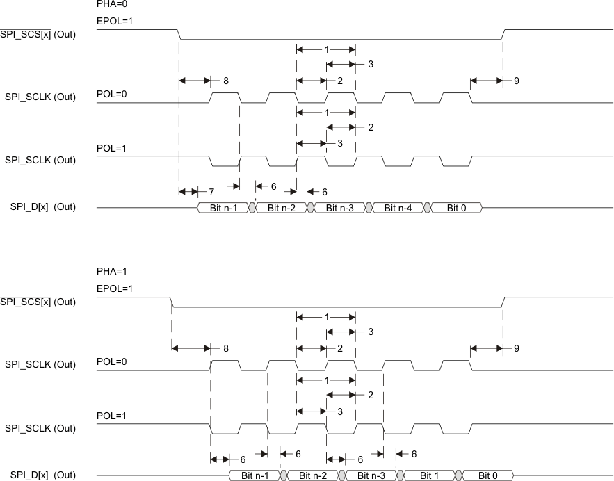 Figure 9-84 SPI Master Mode Transmit Timing
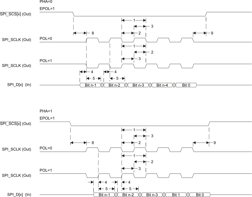 Figure 9-85 SPI Master Mode Receive Timing
Table 9-102 Timing Requirements for SPI - Slave Mode
(see Figure 9-86 and Figure 9-87)| NO. | MIN | MAX | UNIT | ||
|---|---|---|---|---|---|
| 1 | tc(SPICLK) | Cycle time, SPI_CLK(1)(2) | 62.5(3) | ns | |
| 2 | tw(SPICLKL) | Pulse duration, SPI_CLK low(1) | 0.5*P - 3(4) | ns | |
| 3 | tw(SPICLKH) | Pulse duration, SPI_CLK high(1) | 0.5*P - 3(4) | ns | |
| 4 | tsu(MOSI-SPICLK) | Setup time, SPI_D[x] valid before SPI_CLK active edge(1) | 12.92 | ns | |
| 5 | th(SPICLK-MOSI) | Hold time, SPI_D[x] valid after SPI_CLK active edge(1) | 12.92 | ns | |
| 6 | td(SPICLK-MISO) | Delay time, SPI_CLK active edge to SPI_D[x] transition(1) | -4.00 | 17.1 | ns |
| 7 | td(SCS-MISO) | Delay time, SPI_SCS[x] active edge to SPI_D[x] transition(5) | 17.1 | ns | |
| 8 | tsu(SCS-SPICLK) | Setup time, SPI_SCS[x] valid before SPI_CLK first edge(1) | 12.92 | ns | |
| 9 | th(SPICLK-SCS) | Hold time, SPI_SCS[x] valid after SPI_CLK last edge(1) | 12.92 | ns | |
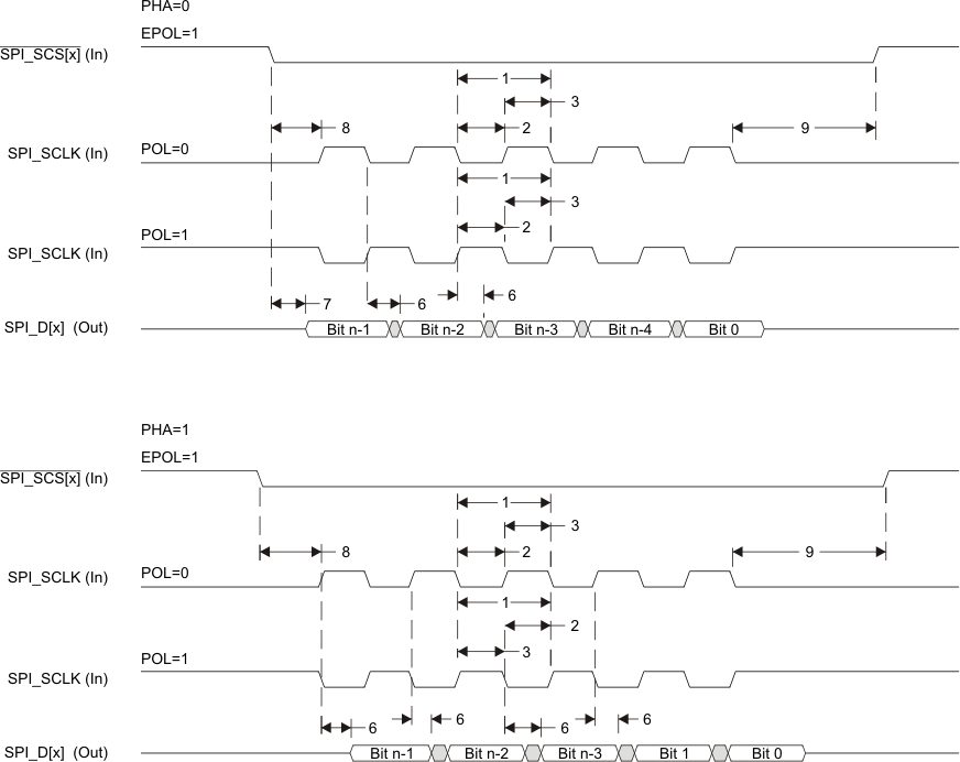 Figure 9-86 SPI Slave Mode Transmit Timing
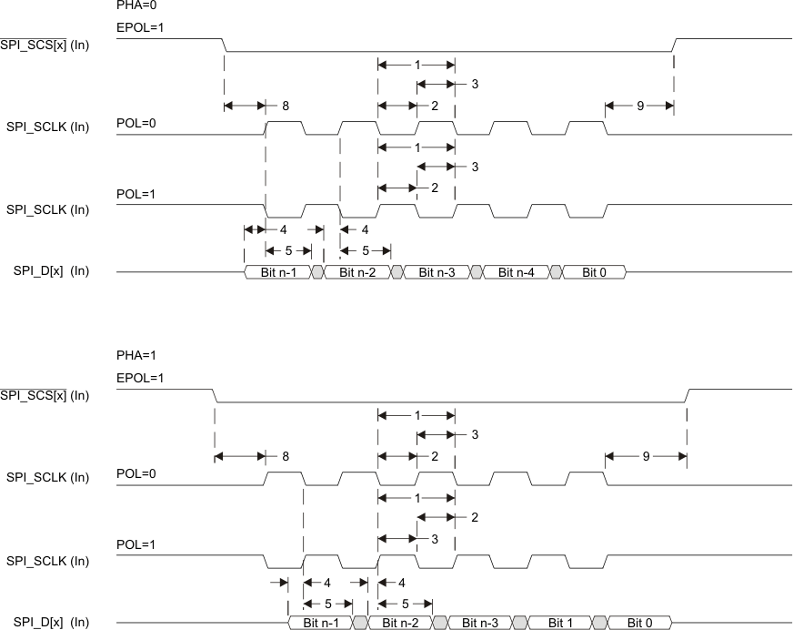 Figure 9-87 SPI Slave Mode Receive Timing
9.19 Timers
The device has seven 32-bit general-purpose (GP) timers that have the following features:
- Timers 1-3 are for software use and do not have an external connection
- Dedicated input trigger for capture mode and dedicated output trigger or pulse width modulation (PWM) signal
- Interrupts generated on overflow, compare, and capture
- Free-running 32-bit upward counter
- Supported modes:
- Compare and capture modes
- Auto-reload mode
- Start-stop mode
- Timer[7:1] functional clock is sourced from either the 27-MHz system clock, 32.768-kHz RTC clock or the TCLKIN external timer input clock, as selected within the PRCM
- On-the-fly read and write register (while counting)
- Generates interrupts to the ARM and DSP CPUs.
The device has one system watchdog timer that has the following features:
- Free-running 32-bit upward counter
- On-the-fly read and write register (while counting)
- Reset upon occurrence of a timer overflow condition
- Two possible clock sources:
- Internal 32.768-kHz clock derived from 27-MHz system clock.
- External clock input on the CLKIN32 input pin.
The watchdog timer is used to provide a recovery mechanism for the device in the event of a fault condition, such as a non-exiting code loop.
For more detailed information, see the Timers chapter in the TMS320DM816x DaVinci Digital Media Processors Technical Reference Manual (literature number SPRUGX8).
9.19.1 Timer Peripheral Register Descriptions
Table 9-103 Timer1-7 Registers(1)
| TIMER1 HEX ADDRESS | TIMER2 HEX ADDRESS | TIMER3 HEX ADDRESS | TIMER4 HEX ADDRESS | TIMER5 HEX ADDRESS | TIMER6 HEX ADDRESS | TIMER7 HEX ADDRESS | ACRONYM | REGISTER NAME |
|---|---|---|---|---|---|---|---|---|
| 0x4802 E000 | 0x4804 0000 | 0x4804 2000 | 0x4804 4000 | 0x4804 6000 | 0x4804 8000 | 0x4804 A000 | TIDR | Identification |
| 0x4802 E010 | 0x4804 0010 | 0x4804 2010 | 0x4804 4010 | 0x4804 6010 | 0x4804 8010 | 0x4804 A010 | TIOCP_CFG | Timer OCP Configuration |
| 0x4802 E020 | 0x4804 0020 | 0x4804 2020 | 0x4804 4020 | 0x4804 6020 | 0x4804 8020 | 0x4804 A020 | IRQ_EOI | Timer IRQ End-Of-Interrupt |
| 0x4802 E024 | 0x4804 0024 | 0x4804 2024 | 0x4804 4024 | 0x4804 6024 | 0x4804 8024 | 0x4804 A024 | IRQSTATUS_RAW | Timer IRQSTATUS Raw |
| 0x4802 E028 | 0x4804 0028 | 0x4804 2028 | 0x4804 4028 | 0x4804 6028 | 0x4804 8028 | 0x4804 A028 | IRQSTATUS | Timer IRQSTATUS |
| 0x4802 E02C | 0x4804 002C | 0x4804 202C | 0x4804 402C | 0x4804 602C | 0x4804 802C | 0x4804 A02C | IRQSTATUS_SET | Timer IRQENABLE Set |
| 0x4802 E030 | 0x4804 0030 | 0x4804 2030 | 0x4804 4030 | 0x4804 6030 | 0x4804 8030 | 0x4804 A030 | IRQSTATUS_CLR | Timer IRQENABLE Clear |
| 0x4802 E034 | 0x4804 0034 | 0x4804 2034 | 0x4804 4034 | 0x4804 6034 | 0x4804 8034 | 0x4804 A034 | IRQWAKEEN | Timer IRQ Wakeup Enable |
| 0x4802 E038 | 0x4804 0038 | 0x4804 2038 | 0x4804 4038 | 0x4804 6038 | 0x4804 8038 | 0x4804 A038 | TCLR | Timer Control |
| 0x4802 E03C | 0x4804 003C | 0x4804 203C | 0x4804 403C | 0x4804 603C | 0x4804 803C | 0x4804 A03C | TCRR | Timer Counter |
| 0x4802 E040 | 0x4804 0040 | 0x4804 2040 | 0x4804 4040 | 0x4804 6040 | 0x4804 8040 | 0x4804 A040 | TLDR | Timer Load |
| 0x4802 E044 | 0x4804 0044 | 0x4804 2044 | 0x4804 4044 | 0x4804 6044 | 0x4804 8044 | 0x4804 A044 | TTGR | Timer Trigger |
| 0x4802 E048 | 0x4804 0048 | 0x4804 2048 | 0x4804 4048 | 0x4804 6048 | 0x4804 8048 | 0x4804 A048 | TWPS | Timer Write Posted Status |
| 0x4802 E04C | 0x4804 004C | 0x4804 204C | 0x4804 404C | 0x4804 604C | 0x4804 804C | 0x4804 A04C | TMAR | Timer Match |
| 0x4802 E050 | 0x4804 0050 | 0x4804 2050 | 0x4804 4050 | 0x4804 6050 | 0x4804 8050 | 0x4804 A050 | TCAR1 | Timer Capture |
| 0x4802 E054 | 0x4804 0054 | 0x4804 2054 | 0x4804 4054 | 0x4804 6054 | 0x4804 8054 | 0x4804 A054 | TSICR | Timer Synchronous Interface Control |
| 0x4802 E058 | 0x4804 0058 | 0x4804 2058 | 0x4804 4058 | 0x4804 6058 | 0x4804 8058 | 0x4804 A058 | TCAR2 | Timer Capture |
Table 9-104 Watchdog Timer Registers
| HEX ADDRESS | ACRONYM | REGISTER NAME |
|---|---|---|
| 0x480C 2000 | WIDR | IP Revision Identifier |
| 0x480C 2010 | WDSC | OCP interface parameters |
| 0x480C 2014 | WDST | Status information |
| 0x480C 2018 | WISR | Interrupt events pending |
| 0x480C 201C | WIER | Interrupt events control |
| 0x480C 2020 | WWER | Wakeup events control |
| 0x480C 2024 | WCLR | Counter prescaler control |
| 0x480C 2028 | WCRR | Internal counter value |
| 0x480C 202C | WLDR | Timer load value |
| 0x480C 2030 | WTGR | Watchdog counter reload |
| 0x480C 2034 | WWPS | Write posting bits |
| 0x480C 2044 | WDLY | Event detection delay value |
| 0x480C 2048 | WSPR | Start-stop value |
| 0x480C 2050 | WIRQEOI | Software End Of Interrupt |
| 0x480C 2054 | WIRQSTATRAW | IRQ unmasked status |
| 0x480C 2058 | WIRQSTAT | IRQ masked status |
| 0x480C 205C | WIRQENSET | IRQ enable |
| 0x480C 2060 | WIRQENCLR | IRQ enable clear |
| 0x480C 2064 | WIRQWAKEEN | IRQ wakeup events control |
9.19.2 Timer Electrical Data and Timing
Table 9-105 Timing Requirements for Timer
(see Figure 9-88)| NO. | MIN | MAX | UNIT | ||
|---|---|---|---|---|---|
| 1 | tw(EVTIH) | Pulse duration, high | 4P(1) | ns | |
| 2 | tw(EVTIL) | Pulse duration, low | 4P(1) | ns | |
Table 9-106 Switching Characteristics Over Recommended Operating Conditions for Timer
(see Figure 9-88)| NO. | PARAMETER | MIN | MAX | UNIT | |
|---|---|---|---|---|---|
| 3 | tw(EVTOH) | Pulse duration, high | 4P-3(1) | ns | |
| 4 | tw(EVTOL) | Pulse duration, low | 4P-3(1) | ns | |
 Figure 9-88 Timer Timing
9.20 Universal Asynchronous Receiver and Transmitter (UART)
The UART performs serial-to-parallel conversions on data received from a peripheral device and parallel-to-serial conversion on data received from the CPU. The device provides up to three UART peripheral interfaces, depending on the selected pin multiplexing.
Each UART has the following features:
- Selectable UART, IrDA (SIR, MIR) and CIR modes
- Dual 64-entry FIFOs for received and transmitted data payload
- Programmable and selectable transmit and receive FIFO trigger levels for DMA and interrupt generation
- Baud-rate generation based upon programmable divisors N (N=1…16384)
- Two DMA requests and one interrupt request to the system
- Can connect to any RS-232 compliant device.
UART functions include:
- Baud-rate up to 3.6 Mbps
- Programmable serial interfaces characteristics
- 5, 6, 7, or 8-bit characters
- Even, odd, or no parity-bit generation and detection
- 1, 1.5, or 2 stop-bit generation
- Flow control: hardware (RTS and CTS) or software (XON and XOFF)
- Additional modem control functions (UART0_DTR, UART0_DSR, UART0_DCD, and UART0_RIN) for UART0 only; UART1 and UART2 do not support full-flow control signaling.
IR-IrDA functions include:
- Support of IrDA 1.4 slow infrared (SIR, baud-rate up to 115.2 Kbps), medium infrared (MIR, baud-rate up to 1.152 Mbps) and fast infrared (FIR baud-rate up to 4.0 Mbps) communications
- Supports framing error, cyclic redundancy check (CRC) error, illegal symbol (FIR), and abort pattern (SIR, MIR) detection
- 8-entry status FIFO (with selectable trigger levels) available to monitor frame length and frame errors.
IR-CIR functions include:
- Consumer infrared (CIR) remote control mode with programmable data encoding
- Free data format (supports any remote control private standards)
- Selectable bit rate and configurable carrier frequency.
For more detailed information on the UART peripheral, see the UART chapter in the TMS320DM816x DaVinci Digital Media Processors Technical Reference Manual (literature number SPRUGX8).
9.20.1 UART Peripheral Register Descriptions
Table 9-107 lists the UART register name summary. Table 9-108 shows the UART registers along with their configuration requirements.
Table 9-107 UART Register Summary
| ACRONYM | REGISTER NAME | ACRONYM | REGISTER NAME |
|---|---|---|---|
| RHR | Receive Holding | RXFLH | Receive Frame Length High |
| THR | Transmit Holding | BLR | BOF Control |
| IER | Interrupt Enable | ACREG | Auxilliary Control |
| IIR | Interrupt Identification | SCR | Supplementary Control |
| FCR | FIFO Control | SSR | Supplementary Status |
| LCR | Line Control | EBLR | BOF Length |
| MCR | Modem Control | MVR | Module Version |
| LSR | Line Status | SYSC | System Configuration |
| MSR | Modem Status | SYSS | System Status |
| SPR | Scratchpad | WER | Wake-up Enable |
| TCR | Transmission Control | CFPS | Carrier Frequency Prescaler |
| TLR | Trigger Level | DLL | Divisor Latch Low |
| MDR1 | Mode Definition 1 | DLH | Divisor Latch High |
| MDR2 | Mode Definition 2 | UASR | UART Autobauding Status |
| SFLSR | Status FIFO Line Status | EFR | Enhanced Feature |
| RESUME | Resume | XON1 | UART XON1 Character |
| SFREGL | Status FIFO Low | XON2 | UART XON2 Character |
| SFREGH | Status FIFO High | XOFF1 | UART XOFF1 Character |
| TXFLL | Transmit Frame Length Low | XOFF2 | UART XOFF2 Character |
| TXFLH | Transmit Frame Length High | ADDR1 | IrDA Address 1 |
| RXFLL | Receive Frame Length Low | ADDR2 | IrDA Address 2 |
Table 9-108 UART Registers Configuration Requirements(1)(2)(3)
| UART0 HEX ADDRESS | UART1 HEX ADDRESS | UART2 HEX ADDRESS | REGISTER | |||||
|---|---|---|---|---|---|---|---|---|
| LCR[7] = 0 | LCR[7] = 1 and LCR[7:0] ≠ 0xBF | LCR[7:0] = 0xBF | ||||||
| READ | WRITE | READ | WRITE | READ | WRITE | |||
| 0x4802 0000 | 0x4802 2000 | 0x4802 4000 | RHR | THR | DLL | DLL | DLL | DLL |
| 0x4802 0004 | 0x4802 2004 | 0x4802 4004 | IER | IER | DLH | DLH | DLH | DLH |
| 0x4802 0008 | 0x4802 2008 | 0x4802 4008 | IIR | FCR | IIR | FCR | EFR | EFR |
| 0x4802 000C | 0x4802 200C | 0x4802 400C | LCR | LCR | LCR | LCR | LCR | LCR |
| 0x4802 0010 | 0x4802 2010 | 0x4802 4010 | MCR | MCR | MCR | MCR | XON1 or ADDR1 |
XON1 or ADDR1 |
| 0x4802 0014 | 0x4802 2014 | 0x4802 4014 | LSR | - | LSR | - | XON2 or ADDR2 |
XON2 or ADDR2 |
| 0x4802 0018 | 0x4802 2018 | 0x4802 4018 | MSR or TCR | TCR | MSR or TCR | TCR | XOFF1 or TCR |
XOFF1 or TCR |
| 0x4802 001C | 0x4802 201C | 0x4802 401C | SPR orTLR | SPR orTLR | SPR or TLR | SPR orTLR | XOFF2 or TLR |
XOFF2 or TLR |
| 0x4802 0020 | 0x4802 2020 | 0x4802 4020 | MDR1 | MDR1 | MDR1 | MDR1 | MDR1 | MDR1 |
| 0x4802 0024 | 0x4802 2024 | 0x4802 4024 | MDR2 | MDR2 | MDR2 | MDR2 | MDR2 | MDR2 |
| 0x4802 0028 | 0x4802 2028 | 0x4802 4028 | SFLSR | TXFLL | SFLSR | TXFLL | SFLSR | TXFLL |
| 0x4802 002C | 0x4802 202C | 0x4802 402C | RESUME | TXFLH | RESUME | TXFLH | RESUME | TXFLH |
| 0x4802 0030 | 0x4802 2030 | 0x4802 4030 | SFREGL | RXFLL | SFREGL | RXFLL | SFREGL | RXFLL |
| 0x4802 0034 | 0x4802 2034 | 0x4802 4034 | SFREGH | RXFLH | SFREGH | RXFLH | SFREGH | RXFLH |
| 0x4802 0038 | 0x4802 2038 | 0x4802 4038 | BLR | BLR | UASR | - | UASR | - |
| 0x4802 003C | 0x4802 203C | 0x4802 403C | ACREG | ACREG | - | - | - | - |
| 0x4802 0040 | 0x4802 2040 | 0x4802 4040 | SCR | SCR | SCR | SCR | SCR | SCR |
| 0x4802 0044 | 0x4802 2044 | 0x4802 4044 | SSR | SSR[2] | SSR | SSR[2] | SSR | SSR[2] |
| 0x4802 0048 | 0x4802 2048 | 0x4802 4048 | EBLR | EBLR | - | - | - | - |
| 0x4802 004C | 0x4802 204C | 0x4802 404C | - | - | - | - | - | - |
| 0x4802 0050 | 0x4802 2050 | 0x4802 4050 | MVR | - | MVR | - | MVR | - |
| 0x4802 0054 | 0x4802 2054 | 0x4802 4054 | SYSC | SYSC | SYSC | SYSC | SYSC | SYSC |
| 0x4802 0058 | 0x4802 2058 | 0x4802 4058 | SYSS | SYSS | SYSS | |||
| 0x4802 005C | 0x4802 205C | 0x4802 405C | WER | WER | WER | WER | WER | WER |
| 0x4802 0060 | 0x4802 2060 | 0x4802 4060 | CFPS | CFPS | CFPS | CFPS | CFPS | CFPS |
| 0x4802 0064 - 0x4802 00C4 | 0x4802 2064 - 0x4802 20C4 | 0x4802 4064 - 0x4802 40C4 | - | - | - | - | - | - |
9.20.2 UART Electrical Data and Timing
Table 9-109 Timing Requirements for UART
(see Figure 9-89)| NO. | MIN | MAX | UNIT | ||
|---|---|---|---|---|---|
| 4 | tw(RX) | Pulse width, receive data bit, 15 pF, 30 pF, 100 pF high or low | 0.96U(1) | 1.05U(1) | ns |
| 5 | tw(CTS) | Pulse width, receive start bit, 15 pF, 30 pF, 100 pF high or low | 0.96U(1) | 1.05U(1) | ns |
| td(RTS-TX) | Delay time, transmit start bit to transmit data | P(2) | ns | ||
| td(CTS-TX) | Delay time, receive start bit to transmit data | P(2) | ns | ||
Table 9-110 Switching Characteristics Over Recommended Operating Conditions for UART
(see Figure 9-89)| NO. | PARAMETER | MIN | MAX | UNIT | ||
|---|---|---|---|---|---|---|
| f(baud) | Maximum programmable baud rate | 15 pF | 5 | MHz | ||
| 30 pF | 0.23 | |||||
| 100 pF | 0.115 | |||||
| 2 | tw(TX) | Pulse width, transmit data bit, 15 pF, 30 pF, 100 pF high or low | U - 2(1) | U + 2(1) | ns | |
| 3 | tw(RTS) | Pulse width, transmit start bit, 15 pF, 30 pF, 100 pF high or low | U - 2(1) | U + 2(1) | ns | |
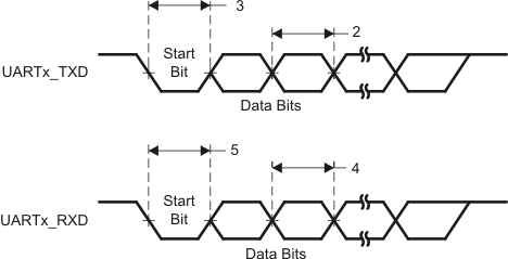 Figure 9-89 UART Timing
9.21 Universal Serial Bus (USB2.0)
The device includes two USB2.0 modules which support the Universal Serial Bus Specification Revision 2.0. The following are some of the major USB features that are supported:
- USB 2.0 peripheral at high speed (HS: 480 Mbps) and full speed (FS: 12 Mbps)
- USB 2.0 host at HS, FS, and low speed (LS: 1.5 Mbps)
- Each endpoint (other than endpoint 0, control only) can support all transfer modes (control, bulk, interrupt, and isochronous)
- Supports high-bandwidth ISO mode
- Supports 16 Transmit (TX) and 16 Receive (RX) endpoints including endpoint 0
- FIFO RAM - 32K endpoint - Programmable size
- Includes two integrated PHYs; requires a low-jitter 24-MHz source clock for its PLL
- RNDIS-like mode for terminating RNDIS-type protocols without using short-packet termination for support of MSC applications.
The USB2.0 modules do not support the following features:
- On-chip charge pump (VBUS power must be generated external to the device)
- RNDIS mode acceleration for USB sizes that are not multiples of 64 bytes
- Endpoint max USB packet sizes that do not conform to the USB2.0 spec (for FS and LS: 8, 16, 32, 64, and 1023 are defined; for HS: 64, 128, 512, and 1024 are defined).
For more detailed information on the USB2.0 peripheral, see the USB2.0 chapter in the TMS320DM816x DaVinci Digital Media Processors Technical Reference Manual (literature number SPRUGX8). For detailed information on USB board design and layout guidelines, see the USB 2.0 Board Design and Layout Guidelines application report (literature number SPRAAR7). For general information on PCB layout, see the DM816xx Easy CYG Package PCB Escape Routing application report (literature number SPRABK6).
9.21.1 USB2.0 Peripheral Register Descriptions
Table 9-111 USB2.0 Submodules
| SUBMODULE ADDRESS OFFSET | SUBMODULE NAME |
|---|---|
| 0x0000 | USBSS registers |
| 0x1000 | USB0 controller registers |
| 0x1800 | USB1 controller registers |
| 0x2000 | CPPI DMA controller registers |
| 0x3000 | CPPI DMA scheduler registers |
| 0x4000 | CPPI DMA Queue Manager registers |
Table 9-112 USB Subsystem (USBSS) Registers(1)
| HEX ADDRESS | ACRONYM | REGISTER NAME |
|---|---|---|
| 0x4740 0000 | REVREG | USBSS REVISION |
| 0x4740 0004 - 0x4740 000C | - | Reserved |
| 0x4740 0010 | SYSCONFIG | USBSS SYSCONFIG |
| 0x4740 0014 - 0x4740 001C | - | Reserved |
| 0x4740 0020 | EOI | USBSS IRQ_EOI |
| 0x4740 0024 | IRQSTATRAW | USBSS IRQ_STATUS_RAW |
| 0x4740 0028 | IRQSTAT | USBSS IRQ_STATUS |
| 0x4740 002C | IRQENABLER | USBSS IRQ_ENABLE_SET |
| 0x4740 0030 | IRQCLEARR | USBSS IRQ_ENABLE_CLR |
| 0x4740 0034 - 0x4740 00FC | - | Reserved |
| 0x4740 0100 | IRQDMATHOLDTX00 | USBSS IRQ_DMA_THRESHOLD_TX0_0 |
| 0x4740 0104 | IRQDMATHOLDTX01 | USBSS IRQ_DMA_THRESHOLD_TX0_1 |
| 0x4740 0108 | IRQDMATHOLDTX02 | USBSS IRQ_DMA_THRESHOLD_TX0_2 |
| 0x4740 010C | IRQDMATHOLDTX03 | USBSS IRQ_DMA_THRESHOLD_TX0_3 |
| 0x4740 0110 | IRQDMATHOLDRX00 | USBSS IRQ_DMA_THRESHOLD_RX0_0 |
| 0x4740 0114 | IRQDMATHOLDRX01 | USBSS IRQ_DMA_THRESHOLD_RX0_1 |
| 0x4740 0118 | IRQDMATHOLDRX02 | USBSS IRQ_DMA_THRESHOLD_RX0_2 |
| 0x4740 011C | IRQDMATHOLDRX03 | USBSS IRQ_DMA_THRESHOLD_RX0_3 |
| 0x4740 0120 | IRQDMATHOLDTX10 | USBSS IRQ_DMA_THRESHOLD_TX1_0 |
| 0x4740 0124 | IRQDMATHOLDTX11 | USBSS IRQ_DMA_THRESHOLD_TX1_1 |
| 0x4740 0128 | IRQDMATHOLDTX12 | USBSS IRQ_DMA_THRESHOLD_TX1_2 |
| 0x4740 012C | IRQDMATHOLDTX13 | USBSS IRQ_DMA_THRESHOLD_TX1_3 |
| 0x4740 0130 | IRQDMATHOLDRX10 | USBSS IRQ_DMA_THRESHOLD_RX1_0 |
| 0x4740 0134 | IRQDMATHOLDRX11 | USBSS IRQ_DMA_THRESHOLD_RX1_1 |
| 0x4740 0138 | IRQDMATHOLDRX12 | USBSS IRQ_DMA_THRESHOLD_RX1_2 |
| 0x4740 013C | IRQDMATHOLDRX13 | USBSS IRQ_DMA_THRESHOLD_RX1_3 |
| 0x4740 0140 | IRQDMAENABLE0 | USBSS IRQ_DMA_ENABLE_0 |
| 0x4740 0144 | IRQDMAENABLE1 | USBSS IRQ_DMA_ENABLE_1 |
| 0x4740 0148 - 0x4740 01FC | - | Reserved |
| 0x4740 0200 | IRQFRAMETHOLDTX00 | USBSS IRQ_FRAME_THRESHOLD_TX0_0 |
| 0x4740 0204 | IRQFRAMETHOLDTX01 | USBSS IRQ_FRAME_THRESHOLD_TX0_1 |
| 0x4740 0208 | IRQFRAMETHOLDTX02 | USBSS IRQ_FRAME_THRESHOLD_TX0_2 |
| 0x4740 020C | IRQFRAMETHOLDTX03 | USBSS IRQ_FRAME_THRESHOLD_TX0_3 |
| 0x4740 0210 | IRQFRAMETHOLDRX00 | USBSS IRQ_FRAME_THRESHOLD_RX0_0 |
| 0x4740 0214 | IRQFRAMETHOLDRX01 | USBSS IRQ_FRAME_THRESHOLD_RX0_1 |
| 0x4740 0218 | IRQFRAMETHOLDRX02 | USBSS IRQ_FRAME_THRESHOLD_RX0_2 |
| 0x4740 021C | IRQFRAMETHOLDRX03 | USBSS IRQ_FRAME_THRESHOLD_RX0_3 |
| 0x4740 0220 | IRQFRAMETHOLDTX10 | USBSS IRQ_FRAME_THRESHOLD_TX1_0 |
| 0x4740 0224 | IRQFRAMETHOLDTX11 | USBSS IRQ_FRAME_THRESHOLD_TX1_1 |
| 0x4740 0228 | IRQFRAMETHOLDTX12 | USBSS IRQ_FRAME_THRESHOLD_TX1_2 |
| 0x4740 022C | IRQFRAMETHOLDTX13 | USBSS IRQ_FRAME_THRESHOLD_TX1_3 |
| 0x4740 0230 | IRQFRAMETHOLDRX10 | USBSS IRQ_FRAME_THRESHOLD_RX1_0 |
| 0x4740 0234 | IRQFRAMETHOLDRX11 | USBSS IRQ_FRAME_THRESHOLD_RX1_1 |
| 0x4740 0238 | IRQFRAMETHOLDRX12 | USBSS IRQ_FRAME_THRESHOLD_RX1_2 |
| 0x4740 023C | IRQFRAMETHOLDRX13 | USBSS IRQ_FRAME_THRESHOLD_RX1_3 |
| 0x4740 0240 | IRQFRAMEENABLE0 | USBSS IRQ_FRAME_ENABLE_0 |
| 0x4740 0244 | IRQFRAMEENABLE1 | USBSS IRQ_FRAME_ENABLE_1 |
| 0x4740 0248 - 0x4740 0FFC | - | Reserved |
Table 9-113 USB0 Controller Registers
| HEX ADDRESS | ACRONYM | REGISTER NAME |
|---|---|---|
| 0x4740 1000 | USB0REV | USB0 REVISION |
| 0x4740 1004 - 0x4740 1010 | - | Reserved |
| 0x4740 1014 | USB0CTRL | USB0 Control |
| 0x4740 1018 | USB0STAT | USB0 Status |
| 0x4740 101C | - | Reserved |
| 0x4740 1020 | USB0IRQMSTAT | USB0 IRQ_MERGED_STATUS |
| 0x4740 1024 | USB0IRQEOI | USB0 IRQ_EOI |
| 0x4740 1028 | USB0IRQSTATRAW0 | USB0 IRQ_STATUS_RAW_0 |
| 0x4740 102C | USB0IRQSTATRAW1 | USB0 IRQ_STATUS_RAW_1 |
| 0x4740 1030 | USB0IRQSTAT0 | USB0 IRQ_STATUS_0 |
| 0x4740 1034 | USB0IRQSTAT1 | USB0 IRQ_STATUS_1 |
| 0x4740 1038 | USB0IRQENABLESET0 | USB0 IRQ_ENABLE_SET_0 |
| 0x4740 103C | USB0IRQENABLESET1 | USB0 IRQ_ENABLE_SET_1 |
| 0x4740 1040 | USB0IRQENABLECLR0 | USB0 IRQ_ENABLE_CLR_0 |
| 0x4740 1044 | USB0IRQENABLECLR1 | USB0 IRQ_ENABLE_CLR_1 |
| 0x4740 1048 - 0x4740 106C | - | Reserved |
| 0x4740 1070 | USB0TXMODE | USB0 Tx Mode |
| 0x4740 1074 | USB0RXMODE | USB0 Rx Mode |
| 0x4740 1078 - 0x4740 107C | - | Reserved |
| 0x4740 1080 | USB0GENRNDISEP1 | USB0 Generic RNDIS Size EP1 |
| 0x4740 1084 | USB0GENRNDISEP2 | USB0 Generic RNDIS Size EP2 |
| 0x4740 1088 | USB0GENRNDISEP3 | USB0 Generic RNDIS Size EP3 |
| 0x4740 108C | USB0GENRNDISEP4 | USB0 Generic RNDIS Size EP4 |
| 0x4740 1090 | USB0GENRNDISEP5 | USB0 Generic RNDIS Size EP5 |
| 0x4740 1094 | USB0GENRNDISEP6 | USB0 Generic RNDIS Size EP6 |
| 0x4740 1098 | USB0GENRNDISEP7 | USB0 Generic RNDIS Size EP7 |
| 0x4740 109C | USB0GENRNDISEP8 | USB0 Generic RNDIS Size EP8 |
| 0x4740 10A0 | USB0GENRNDISEP9 | USB0 Generic RNDIS Size EP9 |
| 0x4740 10A4 | USB0GENRNDISEP10 | USB0 Generic RNDIS Size EP10 |
| 0x4740 10A8 | USB0GENRNDISEP11 | USB0 Generic RNDIS Size EP11 |
| 0x4740 10AC | USB0GENRNDISEP12 | USB0 Generic RNDIS Size EP12 |
| 0x4740 10B0 | USB0GENRNDISEP13 | USB0 Generic RNDIS Size EP13 |
| 0x4740 10B4 | USB0GENRNDISEP14 | USB0 Generic RNDIS Size EP14 |
| 0x4740 10B8 | USB0GENRNDISEP15 | USB0 Generic RNDIS Size EP15 |
| 0x4740 10BC - 0x4740 10CC | - | Reserved |
| 0x4740 10D0 | USB0AUTOREQ | USB0 Auto Req |
| 0x4740 10D4 | USB0SRPFIXTIME | USB0 SRP Fix Time |
| 0x4740 10D8 | USB0TDOWN | USB0 Teardown |
| 0x4740 10DC | - | Reserved |
| 0x4740 10E0 | USB0UTMI | USB0 PHY UTMI |
| 0x4740 10E4 | USB0UTMILB | USB0 MGC UTMI Loopback |
| 0x4740 10E8 | USB0MODE | USB0 Mode |
| 0x4740 10E8 - 0x4740 13FF | - | Reserved |
| 0x4740 1400 - 0x4740 159C | - | USB0 Mentor Core Registers |
| 0x4740 15A0 - 0x4740 17FC | - | Reserved |
Table 9-114 USB1 Controller Registers
| HEX ADDRESS | ACRONYM | REGISTER NAME |
|---|---|---|
| 0x4740 1800 | USB1REV | USB1 Revision |
| 0x4740 1804 - 0x4740 1810 | - | Reserved |
| 0x4740 1814 | USB1CTRL | USB1 Control |
| 0x4740 1818 | USB1STAT | USB1 Status |
| 0x4740 181C | - | Reserved |
| 0x4740 1820 | USB1IRQMSTAT | USB1 IRQ_MERGED_STATUS |
| 0x4740 1824 | USB1IRQEOI | USB1 IRQ_EOI |
| 0x4740 1828 | USB1IRQSTATRAW0 | USB1 IRQ_STATUS_RAW_0 |
| 0x4740 182C | USB1IRQSTATRAW1 | USB1 IRQ_STATUS_RAW_1 |
| 0x4740 1830 | USB1IRQSTAT0 | USB1 IRQ_STATUS_0 |
| 0x4740 1834 | USB1IRQSTAT1 | USB1 IRQ_STATUS_1 |
| 0x4740 1838 | USB1IRQENABLESET0 | USB1 IRQ_ENABLE_SET_0 |
| 0x4740 183C | USB1IRQENABLESET1 | USB1 IRQ_ENABLE_SET_1 |
| 0x4740 1840 | USB1IRQENABLECLR0 | USB1 IRQ_ENABLE_CLR_0 |
| 0x4740 1844 | USB1IRQENABLECLR1 | USB1 IRQ_ENABLE_CLR_1 |
| 0x4740 1848 - 0x4740 186C | - | Reserved |
| 0x4740 1870 | USB1TXMODE | USB1 Tx Mode |
| 0x4740 1874 | USB1RXMODE | USB1 Rx Mode |
| 0x4740 1878 - 0x4740 187C | - | Reserved |
| 0x4740 1880 | USB1GENRNDISEP1 | USB1 Generic RNDIS Size EP1 |
| 0x4740 1884 | USB1GENRNDISEP2 | USB1 Generic RNDIS Size EP2 |
| 0x4740 1888 | USB1GENRNDISEP3 | USB1 Generic RNDIS Size EP3 |
| 0x4740 188C | USB1GENRNDISEP4 | USB1 Generic RNDIS Size EP4 |
| 0x4740 1890 | USB1GENRNDISEP5 | USB1 Generic RNDIS Size EP5 |
| 0x4740 1894 | USB1GENRNDISEP6 | USB1 Generic RNDIS Size EP6 |
| 0x4740 1898 | USB1GENRNDISEP7 | USB1 Generic RNDIS Size EP7 |
| 0x4740 189C | USB1GENRNDISEP8 | USB1 Generic RNDIS Size EP8 |
| 0x4740 18A0 | USB1GENRNDISEP9 | USB1 Generic RNDIS Size EP9 |
| 0x4740 18A4 | USB1GENRNDISEP10 | USB1 Generic RNDIS Size EP10 |
| 0x4740 18A8 | USB1GENRNDISEP11 | USB1 Generic RNDIS Size EP11 |
| 0x4740 18AC | USB1GENRNDISEP12 | USB1 Generic RNDIS Size EP12 |
| 0x4740 18B0 | USB1GENRNDISEP13 | USB1 Generic RNDIS Size EP13 |
| 0x4740 18B4 | USB1GENRNDISEP14 | USB1 Generic RNDIS Size EP14 |
| 0x4740 18B8 | USB1GENRNDISEP15 | USB1 Generic RNDIS Size EP15 |
| 0x4740 18BC - 0x4740 18CC | - | Reserved |
| 0x4740 18D0 | USB1AUTOREQ | USB1 Auto Req |
| 0x4740 18D4 | USB1SRPFIXTIME | USB1 SRP Fix Time |
| 0x4740 18D8 | USB1TDOWN | USB1 Teardown |
| 0x4740 18DC | - | Reserved |
| 0x4740 18E0 | USB1UTMI | USB1 PHY UTMI |
| 0x4740 18E4 | USB1UTMILB | USB1 MGC UTMI Loopback |
| 0x4740 18E8 | USB1MODE | USB1 Mode |
| 0x4740 18E8 - 0x4740 1BFF | - | Reserved |
| 0x4740 1C00 - 0x4740 1D9C | - | USB1 Mentor Core Registers |
| 0x4740 1DA0 - 0x4740 1FFC | - | Reserved |
Table 9-115 CPPI DMA Controller Registers
| HEX ADDRESS | ACRONYM | REGISTER NAME |
|---|---|---|
| 0x4740 2000 | DMAREVID | Revision |
| 0x4740 2004 | TDFDQ | Teardown Free Descriptor Queue Control |
| 0x4740 2008 | DMAEMU | Emulation Control |
| 0x4740 2010 | DMAMEM1BA | CPPI Mem1 Base Address |
| 0x4740 2014 | DMAMEM1MASK | CPPI Mem1 Mask Address |
| 0x4740 200C - 0x4740 27FF | - | Reserved |
| 0x4740 2800 | TXGCR0 | Tx Channel 0 Global Configuration |
| 0x4740 2804 | - | Reserved |
| 0x4740 2808 | RXGCR0 | Rx Channel 0 Global Configuration |
| 0x4740 280C | RXHPCRA0 | Rx Channel 0 Host Packet Configuration A |
| 0x4740 2810 | RXHPCRB0 | Rx Channel 0 Host Packet Configuration B |
| 0x4740 2814 - 0x4740 281C | - | Reserved |
| 0x4740 2820 | TXGCR1 | Tx Channel 1 Global Configuration |
| 0x4740 2824 | - | Reserved |
| 0x4740 2828 | RXGCR1 | Rx Channel 1 Global Configuration |
| 0x4740 282C | RXHPCRA1 | Rx Channel 1 Host Packet Configuration A |
| 0x4740 2830 | RXHPCRB1 | Rx Channel 1 Host Packet Configuration B |
| 0x4740 2834 - 0x4740 283C | - | Reserved |
| 0x4740 2840 | TXGCR2 | Tx Channel 2 Global Configuration |
| 0x4740 2844 | - | Reserved |
| 0x4740 2848 | RXGCR2 | Rx Channel 2 Global Configuration |
| 0x4740 284C | RXHPCRA2 | Rx Channel 2 Host Packet Configuration A |
| 0x4740 2850 | RXHPCRB2 | Rx Channel 2 Host Packet Configuration B |
| 0x4740 2854 - 0x4740 285F | - | Reserved |
| 0x4740 2860 | TXGCR3 | Tx Channel 3 Global Configuration |
| 0x4740 2864 | - | Reserved |
| 0x4740 2868 | RXGCR3 | Rx Channel 3 Global Configuration |
| 0x4740 286C | RXHPCRA3 | Rx Channel 3 Host Packet Configuration A |
| 0x4740 2870 | RXHPCRB3 | Rx Channel 3 Host Packet Configuration B |
| 0x4740 2880 - 0x4740 2B9F | - | ... |
| 0x4740 2BA0 | TXGCR29 | Tx Channel 29 Global Configuration |
| 0x4740 2BA4 | - | Reserved |
| 0x4740 2BA8 | RXGCR29 | Rx Channel 29 Global Configuration |
| 0x4740 2BAC | RXHPCRA29 | Rx Channel 29 Host Packet Configuration A |
| 0x4740 2BB0 | RXHPCRB29 | Rx Channel 29 Host Packet Configuration B |
| 0x4740 2BB4 - 0x4740 2FFF | - | Reserved |
Table 9-116 CPPI DMA Scheduler Registers
| HEX ADDRESS | ACRONYM | REGISTER NAME |
|---|---|---|
| 0x4740 3000 | DMA_SCHED_CTRL | CPPI DMA Scheduler Control Register |
| 0x4740 3804 - 0x4740 38FF | - | Reserved |
| 0x4740 3800 | WORD0 | CPPI DMA Scheduler Table Word 0 |
| 0x4740 3804 | WORD1 | CPPI DMA Scheduler Table Word 1 |
| … | … | … |
| 0x4740 38F8 | WORD62 | CPPI DMA Scheduler Table Word 62 |
| 0x4740 38FC | WORD63 | CPPI DMA Scheduler Table Word 63 |
| 0x4740 38FF - 0x4740 3FFF | - | Reserved |
Table 9-117 CPPI DMA Queue Manager Registers
| HEX ADDRESS | ACRONYM | REGISTER NAME |
|---|---|---|
| 0x4740 4000 | QMGRREVID | Queue Manager Revision |
| 0x4740 4004 | - | Reserved |
| 0x4740 4008 | DIVERSION | Queue Manager Queue Diversion |
| 0x4740 4020 | FDBSC0 | Queue Manager Free Descriptor and Buffer Starvation Count 0 |
| 0x4740 4024 | FDBSC1 | Queue Manager Free Descriptor and Buffer Starvation Count 1 |
| 0x4740 4028 | FDBSC2 | Queue Manager Free Descriptor and Buffer Starvation Count 2 |
| 0x4740 402C | FDBSC3 | Queue Manager Free Descriptor and Buffer Starvation Count 3 |
| 0x4740 4030 | FDBSC4 | Queue Manager Free Descriptor and Buffer Starvation Count 4 |
| 0x4740 4034 | FDBSC5 | Queue Manager Free Descriptor and Buffer Starvation Count 5 |
| 0x4740 4038 | FDBSC6 | Queue Manager Free Descriptor and Buffer Starvation Count 6 |
| 0x4740 403C | FDBSC7 | Queue Manager Free Descriptor and Buffer Starvation Count 7 |
| 0x4740 4030 - 0x4740 407C | - | Reserved |
| 0x4740 4080 | LRAM0BASE | Queue Manager Linking RAM Region 0 Base Address |
| 0x4740 4084 | LRAM0SIZE | Queue Manager Linking RAM Region 0 Size |
| 0x4740 4088 | LRAM1BASE | Queue Manager Linking RAM Region 1 Base Address |
| 0x4740 408C | - | Reserved |
| 0x4740 4090 | PEND0 | Queue Manager Queue Pending 0 |
| 0x4740 4094 | PEND1 | Queue Manager Queue Pending 1 |
| 0x4740 4098 | PEND2 | Queue Manager Queue Pending 2 |
| 0x4740 409C | PEND3 | Queue Manager Queue Pending 3 |
| 0x4740 40A0 | PEND4 | Queue Manager Queue Pending 4 |
| 0x4740 40A4 - 0x4740 4FFF | - | Reserved |
| 0x4740 5000 + 16xR | QMEMRBASEr | Memory Region R Base Address (R ranges from 0 to 15) |
| 0x4740 5000 + 16xR + 4 | QMEMRCTRLr | Memory Region R Control (R ranges from 0 to 15) |
| 0x4740 50F8 - 0x4740 5FFF | - | Reserved |
| 0x4740 6000 + 16xN | CTRLAn | Queue N Register A (N ranges from 0 to 155) |
| 0x4740 6004 + 16xN | CTRLBn | Queue N Register B (N ranges from 0 to 155) |
| 0x4740 6008 + 16xN | CTRLCn | Queue N Register C (N ranges from 0 to 155) |
| 0x4740 600C + 16xN | CTRLDn | Queue N Register D (N ranges from 0 to 155) |
| 0x4740 69C0 - 0x4740 6FFF | - | Reserved |
| 0x4740 7000 + 16xN | QSTATAn | Queue N Status A (N ranges from 0 to 155) |
| 0x4740 7004 + 16xN | QSTATBn | Queue N Status B (N ranges from 0 to 155) |
| 0x4740 7008 + 16xN | QSTATCn | Queue N Status C (N ranges from 0 to 155) |
| 0x4740 700C + 16xN | - | Reserved |
| 0x4740 79C0 - 0x4740 7FFF | - | Reserved |
9.21.2 USB2.0 Electrical Data and Timing
Table 9-118 Switching Characteristics Over Recommended Operating Conditions for USB2.0
(see Figure 9-90)| NO. | PARAMETER | LOW SPEED 1.5 Mbps |
FULL SPEED 12 Mbps |
HIGH SPEED 480 Mbps |
UNIT | ||||
|---|---|---|---|---|---|---|---|---|---|
| MIN | MAX | MIN | MAX | MIN | MAX | ||||
| 1 | tr(D) | Rise time, USB_DP and USB_DN signals(1) | 75 | 300 | 4 | 20 | 0.5 | ns | |
| 2 | tf(D) | Fall time, USB_DP and USB_DN signals(1) | 75 | 300 | 4 | 20 | 0.5 | ns | |
| 3 | trfM | Rise and Fall time, matching(2) | 80 | 125 | 90 | 111.11 | – | – | % |
| 4 | VCRS | Output signal cross-over voltage(1) | 1.3 | 2 | 1.3 | 2 | – | – | V |
| 5 | tjr(source)NT | Source (Host) Driver jitter, next transition | 2 | 2 | (4) | ns | |||
| tjr(FUNC)NT | Function Driver jitter, next transition | 25 | 2 | (4) | ns | ||||
| 6 | tjr(source)PT | Source (Host) Driver jitter, paired transition(3) | 1 | 1 | (4) | ns | |||
| tjr(FUNC)PT | Function Driver jitter, paired transition | 10 | 1 | (4) | ns | ||||
| 7 | tw(EOPT) | Pulse duration, EOP transmitter | 1250 | 1500 | 160 | 175 | – | – | ns |
| 8 | tw(EOPR) | Pulse duration, EOP receiver | 670 | 82 | – | ns | |||
| 9 | t(DRATE) | Data Rate | 1.5 | 12 | 480 | Mb per s | |||
| 10 | ZDRV | Driver Output Resistance | – | – | 28 | 49.5 | 40.5 | 49.5 | Ω |
| 11 | USB_R1 | USB reference resistor | 43.8 | 44.6 | 43.8 | 44.6 | 43.8 | 44.6 | Ω |
 Figure 9-90 USB2.0 Integrated Transceiver Interface Timing
