SLVSBR1F January 2013 – January 2015 TPD4S214
PRODUCTION DATA.
- 1 Features
- 2 Applications
- 3 Description
- 4 Simplified Schematic
- 5 Revision History
- 6 Pin Configuration and Functions
-
7 Specifications
- 7.1 Absolute Maximum Ratings
- 7.2 ESD Ratings
- 7.3 Recommended Operating Conditions
- 7.4 Thermal Information
- 7.5 Thermal Shutdown
- 7.6 Electrical Characteristics for EN, FLT, DET, D+, D-, VBUS, ID Pins
- 7.7 Electrical characteristics for UVLO / OVLO
- 7.8 Electrical Characteristics for DET Circuits
- 7.9 Electrical Characteristics for OTG Switch
- 7.10 Electrical Characteristics for Current Limit and Short Circuit Protection
- 7.11 Supply Current Consumption
- 7.12 Typical Characteristics
-
8 Detailed Description
- 8.1 Overview
- 8.2 Functional Block Diagram
- 8.3
Feature Description
- 8.3.1 Input Voltage Protection at VBUS from -7 V to 30 V
- 8.3.2 IEC 61000-4-2 Level 4 ESD Protection
- 8.3.3 Low RDS(ON) N-CH FET Switch for High Efficiency
- 8.3.4 Compliant with USB2.0 and USB3.0 OTG spec
- 8.3.5 User Adjustable Current Limit From 250 mA to Beyond 1.2 A
- 8.3.6 Built-in Soft-start
- 8.3.7 Reverse Current Blocking
- 8.3.8 Over Voltage Lock Out for VBUS
- 8.3.9 Under Voltage Lock Out for VOTG_IN
- 8.3.10 Thermal Shutdown and Short Circuit Protection
- 8.3.11 Auto Retry on any Fault; no Latching off States
- 8.3.12 Integrated VBUS Detection Circuit
- 8.3.13 Low Capacitance TVS ESD Clamp for USB2.0 High Speed Data Rate
- 8.3.14 Internal 16ms Startup Delay
- 8.3.15 Space Saving WCSP (12-YFF) Package
- 8.3.16 Inrush Current Protection
- 8.3.17 Input Capacitor (Optional)
- 8.3.18 Output Capacitor (Optional)
- 8.3.19 Current Limit
- 8.3.20 Thermal Shutdown
- 8.3.21 VBUS Detection
- 8.3.22 Test Configuration
- 8.4 Device Functional Modes
- 9 Application and Implementation
- 10Power Supply Recommendations
- 11Layout
- 12Device and Documentation Support
- 13Mechanical, Packaging, and Orderable Information
9 Application and Implementation
NOTE
Information in the following applications sections is not part of the TI component specification, and TI does not warrant its accuracy or completeness. TI’s customers are responsible for determining suitability of components for their purposes. Customers should validate and test their design implementation to confirm system functionality.
9.1 Application Information
A USB OTG device’s one and only connector is the AB receptacle, which accepts either an A or B plug. When an A-plug is inserted, the OTG device is called the A-device and when a B-plug is inserted it is called the B-device. A-device is often times referred to as “Targeted Host” and B-device as “USB peripheral”. TPD4S214 supports an OTG device when TPD4S214’s system is acting as an A-device and powering the USB interface. The TPD4S214 may also be used in non-OTG applications where it resides on the current source side.
9.2 Typical Application
The TPD4S214 is placed next to the USB connector to provide over voltage, over current, and ESD protection for the OTG 5-V source and USB Controller.
9.2.1 USB 2.0 Without Using On-chip VBUS Detect
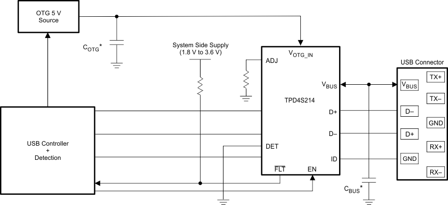
An example using TPD4S214 to protect an OTG 5-V source and USB 2.0 Controller is shown below. This USB Controller does not utilize VBUS detection with the DET pin, so DET is tied to GND. TPD4S214 is placed in the transmitter channel immediately adjacent to the USB connector. The D+, D-, ID pins on TPD4S214 are interchangeable so that each can protect either of the D+, D-, ID pins on the USB connector, the naming convention is just a suggestion.
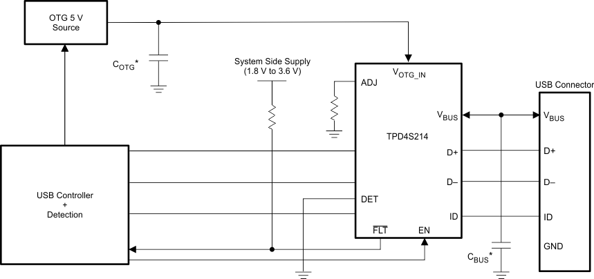 Figure 24. USB2.0 Application Diagram Without Using On-chip VBUS Detect
*COTG and CBUS have minimum recommended values of 1 µF each
9.2.1.1 Design Requirements
For this example, use the following table as input parameters:
| Design Parameters | Example Value |
|---|---|
| Signal range on VOTG_IN | 3.8 V – 5.5 V |
| Signal range on VBUS | 0 V – 5.3 V nominal, withstand -7 V to 30 V |
| IBUS_MAX | 500 mA |
| RADJ | 100 kΩ |
| Drive EN low (disabled) | 0 V – 0.4 V |
| Drive EN high (enabled) | 1.2 V – 5.5 V |
9.2.1.2 Detailed Design Procedure
To begin the design process, determine the maximum current expected under normal usage. In this example, the maximum expected current is 500 mA so an RADJ of 100 kΩ was selected to begin current limiting at around 550 mA and protect the OTG system. Fault conditions are monitored by the USB controller by using the FLT Pin. DET is not used and is grounded and can optionally be left floating instead.
9.2.1.3 Application Curves
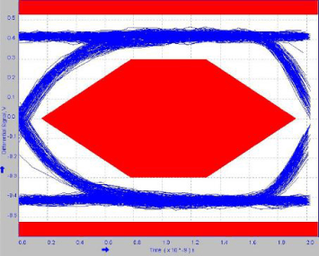 Figure 25. Eye Diagram with no EVM and no IC, Full USB2.0 Speed at 480 Mbps
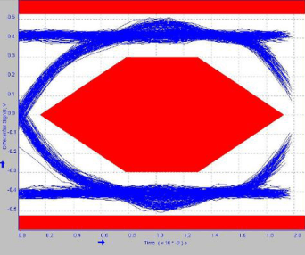 Figure 27. Eye Diagram with TPD4S214EVM and IC, Full USB2.0 Speed at 480 Mbps
 Figure 26. Eye Diagram with TPD4S214EVM but no IC, Full USB2.0 Speed at 480 Mbps
9.2.2 USB 2.0 Using On-chip VBUS Detect
An example using TPD4S214 to protect an OTG 5-V source and USB 2.0 Controller is shown below. This USB Controller monitors VBUS detection with the DET pin. This can be advantageous when a peripheral with an Embedded Host is attached. In this case, if there is a valid voltage present on VBUS there is no need to provide OTG power, so the USB Controller can be programmed to disable the OTG 5-V source, resulting in a power savings. The D+, D-, ID pins on TPD4S214 are interchangeable so that each can protect either of the D+, D-, ID pins on the USB connector, the naming convention is just a suggestion.
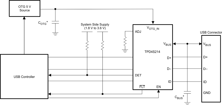 Figure 28. USB 2.0 Application Diagram Using On-chip VBUS Detect
*COTG and CBUS each have minimum recommended values of 1 µF
9.2.2.1 Design Requirements
For this example, use the following table as input parameters:
| Design Parameters | Example Value |
|---|---|
| Signal range on VOTG_IN | 3.8 V – 5.5 V |
| Signal range on VBUS | 0 V – 5.3 V nominal, withstand –7 V to 30 V |
| IBUS_MAX | 500 mA |
| RADJ | 100 kΩ |
| Drive EN low (disabled) | 0 V – 0.4 V |
| Drive EN high (enabled) | 1.2 V – 5.5 V |
9.2.2.2 Detailed Design Procedure
To begin the design process, determine the maximum current expected under normal usage. In this example, the maximum expected current is 500 mA so an RADJ of 100 kΩ was selected to begin current limiting at around 550 mA and protect the OTG system. Fault conditions are monitored by the USB controller by using the FLT Pin. DET Pin is used to facilitate detecting between a USB host and peripheral device on VBUS.
9.2.2.3 Application Curves
Refer to Application Curves for related application curves.
9.2.3 USB 3.0 Without Using On-chip VBUS Detect
An example using TPD4S214 to protect an OTG 5-V source and USB 3.0 Controller is shown below. This USB Controller does not utilize VBUS detection with the DET pin, so it is tied to GND. The D+, D-, ID pins on TPD4S214 are interchangeable so that each can protect either of the D+, D-, ID pins on the USB connector, the naming convention is just a suggestion.
9.2.3.1 Design Requirements
For this example, use the following table as input parameters:
| Design Parameters | Example Value |
|---|---|
| Signal range on VOTG_IN | 3.8 V – 5.5 V |
| Signal range on VBUS | 0 V – 5.3 V nominal, withstand –7 V to 30 V |
| IBUS_MAX | 900 mA |
| RADJ | 56 kΩ |
| Drive EN low (disabled) | 0 V – 0.4 V |
| Drive EN high (enabled) | 1.2 V – 5.5 V |
9.2.3.2 Detailed Design Procedure
To begin the design process, determine the maximum current expected under normal usage. In this example, the maximum expected current is 900 mA so an RADJ of 56 kΩ was selected to begin current limiting at around 1 A and protect the OTG system. Fault conditions are monitored by the USB controller by the FLT Pin. DET is not used and is grounded and can optionally be left floating instead.
9.2.3.3 Application Curves
Refer to Application Curves for related application curves.