SLVSBR1F January 2013 – January 2015 TPD4S214
PRODUCTION DATA.
- 1 Features
- 2 Applications
- 3 Description
- 4 Simplified Schematic
- 5 Revision History
- 6 Pin Configuration and Functions
-
7 Specifications
- 7.1 Absolute Maximum Ratings
- 7.2 ESD Ratings
- 7.3 Recommended Operating Conditions
- 7.4 Thermal Information
- 7.5 Thermal Shutdown
- 7.6 Electrical Characteristics for EN, FLT, DET, D+, D-, VBUS, ID Pins
- 7.7 Electrical characteristics for UVLO / OVLO
- 7.8 Electrical Characteristics for DET Circuits
- 7.9 Electrical Characteristics for OTG Switch
- 7.10 Electrical Characteristics for Current Limit and Short Circuit Protection
- 7.11 Supply Current Consumption
- 7.12 Typical Characteristics
-
8 Detailed Description
- 8.1 Overview
- 8.2 Functional Block Diagram
- 8.3
Feature Description
- 8.3.1 Input Voltage Protection at VBUS from -7 V to 30 V
- 8.3.2 IEC 61000-4-2 Level 4 ESD Protection
- 8.3.3 Low RDS(ON) N-CH FET Switch for High Efficiency
- 8.3.4 Compliant with USB2.0 and USB3.0 OTG spec
- 8.3.5 User Adjustable Current Limit From 250 mA to Beyond 1.2 A
- 8.3.6 Built-in Soft-start
- 8.3.7 Reverse Current Blocking
- 8.3.8 Over Voltage Lock Out for VBUS
- 8.3.9 Under Voltage Lock Out for VOTG_IN
- 8.3.10 Thermal Shutdown and Short Circuit Protection
- 8.3.11 Auto Retry on any Fault; no Latching off States
- 8.3.12 Integrated VBUS Detection Circuit
- 8.3.13 Low Capacitance TVS ESD Clamp for USB2.0 High Speed Data Rate
- 8.3.14 Internal 16ms Startup Delay
- 8.3.15 Space Saving WCSP (12-YFF) Package
- 8.3.16 Inrush Current Protection
- 8.3.17 Input Capacitor (Optional)
- 8.3.18 Output Capacitor (Optional)
- 8.3.19 Current Limit
- 8.3.20 Thermal Shutdown
- 8.3.21 VBUS Detection
- 8.3.22 Test Configuration
- 8.4 Device Functional Modes
- 9 Application and Implementation
- 10Power Supply Recommendations
- 11Layout
- 12Device and Documentation Support
- 13Mechanical, Packaging, and Orderable Information
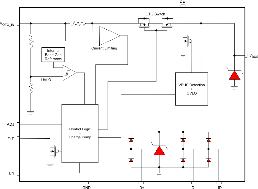
8 Detailed Description
8.1 Overview
The TPD4S214 is a single-chip protection solution for USB On-the-Go and other current limited USB applications. This device includes an integrated low RDS(ON) N-channel current limited switch for OTG current supply to peripheral devices. TPD4S214 offers low capacitance TVS ESD clamps for the D+, D–, and ID pins for both USB2.0 and USB3.0 applications. The VBUS pin can handle continuous voltage ranging from –7 V to 30 V. The OVLO at the VBUS pin ensures that if there is a fault condition at the VBUS line, TPD4S214 is able to isolate it and protect the internal circuitry from damage. Similarly, the UVLO at the VOTG_IN pin ensures that there is no power drain from the internal OTG supply to external VBUS if VOTG_IN droops below a safe operating level.
When EN is high, the OTG switch is activated and the FLT pin indicates whether there is a fault condition. The soft start feature waits 16 ms to turn on the OTG switch after all operating conditions are met. The FLT pin asserts low during any one of the following fault conditions: OVLO (VBUS > VOVLO), UVLO condition (VOTG_IN < VUVLO) over temperature, over current, short circuit condition, or reverse-current-condition (VBUS > VOTG_IN). The OTG switch is turned off during any fault condition. Once the switch is turned off, the IC periodically rechecks the faults internally. If the IC returns to normal operating conditions, the switch turns back on and FLT is reset to high.
There is also a VBUS detection feature for facilitating USB communication between USB host and peripheral device. If this is not used, the DET pin can be either floating or connected to ground.
8.2 Functional Block Diagram
8.3 Feature Description
8.3.1 Input Voltage Protection at VBUS from –7 V to 30 V
The VBUS pin can handle continuous voltage ranging from –7 V to 30 V. The OVLO at the VBUS pin ensures that if there is a fault condition at the VBUS line, TPD4S214 is able to isolate the fault and protect the internal circuitry from damage.
8.3.2 IEC 61000-4-2 Level 4 ESD Protection
The I/O pins can withstand ESD events up to ±15-kV contact and air gap. An ESD clamp diverts the current to ground.
8.3.3 Low RDS(ON) N-CH FET Switch for High Efficiency
A Low RDS(ON) ensures there is minimal voltage loss when supplying high current to OTG devices.
8.3.4 Compliant with USB2.0 and USB3.0 OTG spec
The capability of TPD4S214 to supply greater than 1.2 A of current on VBUS meets or exceeds the USB2.0 and USB3.0 OTG specification.
8.3.5 User Adjustable Current Limit From 250 mA to Beyond 1.2 A
The designer can select the over current protection level by selecting the proper RADJ.
8.3.6 Built-in Soft-start
The soft start feature waits 16 ms to turn on the OTG switch after all operating conditions are met.
8.3.7 Reverse Current Blocking
If VBUS is greater than VOTG_IN by 50 mV, the OTG switch is disabled in 17.5 ms.
8.3.8 Over Voltage Lock Out for VBUS
OVLO ensures that an over voltage condition on VBUS disables the OTG switch to protect the system.
8.3.9 Under Voltage Lock Out for VOTG_IN
UVLO ensures that an under voltage condition on VBUS disables the OTG switch to protect the system.
8.3.10 Thermal Shutdown and Short Circuit Protection
TPD4S214 has an over-temperature protection circuit to protect against system faults or improper use. The basic function of the thermal shutdown (TSD) circuit is to sense when the junction temperature has exceeded the absolute maximum rating and shut down the device until the junction temperature has cooled to a safe level. Short circuit protection prevents any damaging current demand from the system.
8.3.11 Auto Retry on any Fault; no Latching off States
In any fault condition, TPD4S214 will reassess VBUS, VOTG_IN, and thermal conditions until a safe state is reached and then enable the OTG switch, eliminating any latched off states.
8.3.12 Integrated VBUS Detection Circuit
TPD4S214 has a VBUS detection feature facilitating communication between the USB host and peripheral device. The use of this feature is optional.
8.3.13 Low Capacitance TVS ESD Clamp for USB2.0 High Speed Data Rate
The High Speed data lines have a capacitance less than 2 pF, supporting a bandwidth greater than 3 GHz. This easily accommodates the 480-Mbps data rate defined in the USB2.0 specification.
8.3.14 Internal 16ms Startup Delay
The built-in start up delay allows for voltages on VBUS to reach a steady state after which a 1-μA trickle charge slowly turns on the main switch. During the inrush period, the peak inrush current will be limited to no more than the current limit set by the external resistor RADJ.
8.3.15 Space Saving WCSP (12-YFF) Package
The 1.69 mm × 1.39 mm (Max) WCSP package is valuable in space constrained designs.
8.3.16 Inrush Current Protection
As soon as TPD4S214 is enabled, its logic block detects the presence of any fault conditions highlighted in Table 2. In the absence of any fault condition, a counter waits for 16 ms, after which a 1-µA trickle charge slowly turns on the main switch. During the inrush period, the peak inrush current will be limited to no more than the current limit set by the external resistor RADJ.
8.3.17 Input Capacitor (Optional)
To limit the voltage drop on the input supply caused by transient in-rush currents when the switch turns on into a discharged load capacitor or short-circuit, a capacitor needs to be placed between VOTG_IN and GND. A 10-μF ceramic capacitor, CIN, placed close to the pins, is usually sufficient. Higher values of CIN can be used to further reduce the voltage drop during high-current application. When switching heavy loads, it is recommended to have an input capacitor about 10 times higher than the output capacitor to avoid excessive voltage drop.
8.3.18 Output Capacitor (Optional)
Due to the integrated body diode in the NMOS switch, a CIN greater than CLOAD is highly recommended. A CLOAD greater than CIN can cause VBUS to exceed VOTG_IN when the system supply is removed. A CIN to CLOAD ratio of 10 to 1 is recommended for minimizing VOTG_IN dip caused by inrush currents during startup.
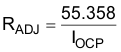
8.3.19 Current Limit
The TPD4S214 provides current limiting protection, which is set by an external resistor connected from the ADJ pin to ground shown in Figure 18. The current limiting threshold IOCP is set by the external resistor RADJ. Figure 19 shows the typical current limit for a corresponding RADJ value with ±1% tolerance across the operating temperature range.
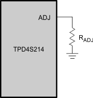 Figure 18. Current Limit Diagram
Where:
RADJ = external resistor used to set the current limit (kΩ)
IOCP = current limit set by the external RADJ resistor (A)
RADJ is placed between the ADJ pin and ground, shown in Figure 18, providing a maximum current limit between 250 mA and 1.2 A.
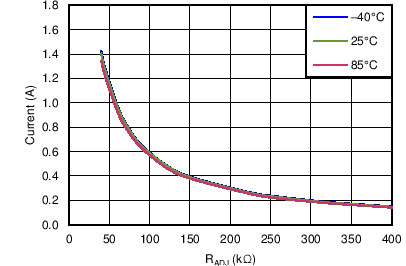 Figure 19. IOCP versus RADJ
 Figure 20. IBUS Temperature Derating Curve
The temperature derating curve shown in Figure 20 graphs the line where TPD4S214 will have a Mean Time Before Failure (MTBF) of 5 years at a 100% duty cycle for a given junction temperature, Tj, and current on VBUS, or IBUS. MTBF of 5 years at a 100% duty cycle is equivalent to 7.5 years at a 75% duty cycle, or 10 years at a 50% duty cycle. See Equation 2 to calculate the junction temperature. If a current and junction temperature point lie below the curve on the graph then the MTBF will exceed 5 years at a 100% duty cycle, or its equivalent. If above the curve, the MTBF will be decreased.
8.3.20 Thermal Shutdown
When the device is ON, current flowing through the device will cause the device to heat up. Overheating can lead to permanent damage to the device. To prevent this, an over temperature protection has been designed into the device. Whenever the junction temperature exceeds 141ºC, the switch will turn off, thereby limiting the temperature. Once the device cools down to below 125ºC the switch will turn on if the EN is active and the VBUS voltage is within the UVLO and OVP thresholds. While the over temperature protection in the device will not kick-in unless the die temperature reaches 141ºC, it is generally recommended that care is taken to keep the junction temperature below 125ºC. Operation of the device above 125ºC for extended periods of time can affect the long-term reliability of the part.
The junction temperature of the device can be calculated using the below formula:
Where:
| Tj = Junction temperature | ||
| TA = Ambient temperature | ||
| RθJA = Thermal resistance | ||
| PD = Power Dissipated in device |
| I = Current through device | ||
| RDS(ON) = Max on resistance of device |
Example
At 0.5 A, the continuous current power dissipation is given by:
If the ambient temperature is about 85 °C the junction temperature will be:
This implies that, at an ambient temperature of 85ºC, TPD4S214 can pass a continuous 0.5 A without sustaining damage. Conversely, the above calculation can also be used to calculate the total continuous current the TPD4S214 can handle at any given temperature.
The MTBF can be estimated by examining Figure 20. Locating 0.5 A and 91.7 °C, the point is below the curve. This implies that the MTBF for this calculation is longer than 5 years at a 100% duty cycle. If the duty cycle is 50% then MTBF exceeds 10 years.
8.3.21 VBUS Detection
There are several important protocols defined in [OTG and EH Supplement] that governs communication between Targeted Hosts (A-device) and USB peripherals (B-device). Communication between host and peripheral is usually done on the ID pin only. In the case when two OTG devices that could both act as either host or peripheral are connected, measuring voltage level on VBUS will aid in the handshaking process. If an embedded host instead of a USB peripheral is connected to the OTG device, OTG charging would not be required and the system’s OTG source should remain off to conserve power. The TPD4S214 VBUS detection block aids power conservation and is powered from VBUS. See Functional Block Diagram. The DET pin is an open drain PMOS output with default state low.
In the event when an A-plug is attached, the system detects ID pin as FALSE, in which case ID pin resistance to ground is less than 10 Ω. For a B-plug, the system detects ID pin as TRUE and ID pin resistance to ground is greater than 100 kΩ. For the system to power a USB device through OTG switch once it is connected, voltage on VBUS should remain below VBUS_VALID MIN within TA_VBUS_ATT of the ID pin becoming FALSE. After this event, the system confirms that the USB device requires power and enables both TPD4S214 and OTG source. However, if VBUS_VALID is detected on VBUS within TA_VBUS_ATT of the ID pin becoming FALSE, there is either a system error or the device connected does not require charging. OTG source remains switched off and the entire sequence would restart when the system detects another FALSE on the ID pin.
Table 1. VBUS Detection scheme
| EN | VOTG_IN (VBUS Detect Power) | VBUS | DET | Condition |
|---|---|---|---|---|
| X | X | VBUS_VALID– < VBUS < VBUS_VALID+ | H | VBUS within VBUS_VALID |
| X | X | VBUS_VALID– > VBUS or VBUS > VBUS_VALID+ | L | VBUS outside of VBUS_VALID |
X = Don’t Care, H = Signal High, and L = Signal Low
Figure 21 and Figure 22 shows suggested system level timing diagrams for detecting VBUS according to [OTG and EH Supplement]. Figure 28 shows the application diagram. In Figure 21, DET pin remains low after ID pin becomes FALSE, indicating there is not an active voltage source on VBUS. The USB controller proceeds to turn on OTG 5-V source and the TPD4S214 respectively; this sequence is recommended because TPD4S214 is powered through the OTG source. After a period of tON, current starts to flow through the OTG switch and VBUS is ramped to the voltage level of VOTG_IN.
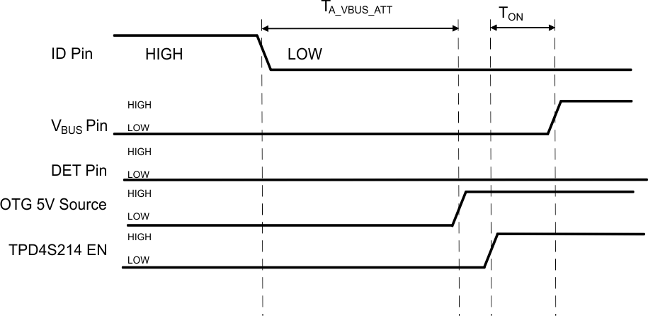 Figure 21. Timing Diagram for Valid USB Device
In Figure 22, DET pin toggles high after an active voltage is detected on VBUS within TA_VBUS_ATT. This indicates that the USB device attached is not suitable for OTG charging and both OTG 5-V source and TPD4S214 remain off.
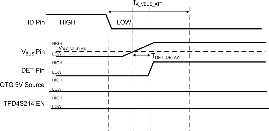 Figure 22. System Level Timing Diagram for invalid USB Device
8.3.22 Test Configuration
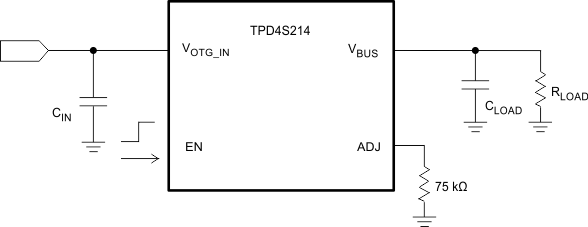 Figure 23. Inrush Current Test Configuration.
Enable is toggled from low to high. See the Application Information section for CIN and CLOAD value recommendations.
8.4 Device Functional Modes
Table 2. Device Operation
| EN | VOTG_IN | VBUS | OCP | OTP | OTG SW | FLT | FAULT CONDITION |
|---|---|---|---|---|---|---|---|
| X | 0 | 0 | F | F | OFF | L | SW Disabled |
| X | X | X | X | T | OFF | L | Over Temperature |
| H | X | X | T | X | OFF | L | Over Current |
| H | VOTG_IN > VUVLO | VBUS > VOTG_IN | F | F | OFF | L | Reverse-current |
| H | X | VBUS > VOVLO | F | F | OFF | L | VBUS over-voltage |
| H | VOTG_IN < VUVLO | X | F | F | OFF | L | VOTG_IN under-voltage |
| H | VOTG_IN > VBUS and VOTG_IN > VUVLO |
VSHORT < VBUS < VOTG_IN and VSHORT < VBUS < VOVLO |
F | F | ON | H | Normal (SW Enabled) |