SLVSA05B August   2009  – August 2015 TPS61086

PRODUCTION DATA.  

  1. Features
  2. Applications
  3. Description
  4. Revision History
  5. Pin Configuration and Functions
  6. Specifications
    1. 6.1 Absolute Maximum Ratings
    2. 6.2 ESD Ratings
    3. 6.3 Recommended Operating Conditions
    4. 6.4 Thermal Information
    5. 6.5 Electrical Characteristics
    6. 6.6 Typical Characteristics
  7. Detailed Description
    1. 7.1 Overview
    2. 7.2 Functional Block Diagram
    3. 7.3 Feature Description
      1. 7.3.1 Soft-Start
      2. 7.3.2 Undervoltage Lockout (UVLO)
      3. 7.3.3 Thermal Shutdown
      4. 7.3.4 Overvoltage Prevention
    4. 7.4 Device Functional Modes
      1. 7.4.1 Power Save Mode
      2. 7.4.2 Forced PWM Mode
  8. Application and Implementation
    1. 8.1 Application Information
    2. 8.2 Typical Applications
      1. 8.2.1 3.3-V to 12-V Boost Converter With PFM Mode at Light Load
        1. 8.2.1.1 Design Requirements
        2. 8.2.1.2 Detailed Design Procedure
          1. 8.2.1.2.1 Inductor Selection
          2. 8.2.1.2.2 Rectifier Diode Selection
          3. 8.2.1.2.3 Setting the Output Voltage
          4. 8.2.1.2.4 Compensation (COMP)
          5. 8.2.1.2.5 Input Capacitor Selection
          6. 8.2.1.2.6 Output Capacitor Selection
        3. 8.2.1.3 Application Curves
      2. 8.2.2 3.3-V to 12-V Boost Converter With Forced PWM Mode at Light Load
        1. 8.2.2.1 Design Requirements
        2. 8.2.2.2 Detailed Design Procedure
        3. 8.2.2.3 Application Curves
    3. 8.3 System Examples
  9. Power Supply Recommendations
  10. 10Layout
    1. 10.1 Layout Guidelines
    2. 10.2 Layout Example
  11. 11Device and Documentation Support
    1. 11.1 Community Resources
    2. 11.2 Trademarks
    3. 11.3 Electrostatic Discharge Caution
    4. 11.4 Glossary
  12. 12Mechanical, Packaging, and Orderable Information

パッケージ・オプション

メカニカル・データ(パッケージ|ピン)
サーマルパッド・メカニカル・データ

1 Features

  • 2.3-V to 6.0-V Input Voltage Range
  • 18.5-V Boost Converter With 2.0-A Switch Current
  • 1.2-MHz Switching Frequency
  • Power Save Mode for Improved Efficiency at Low-Output Power or Forced PWM
  • Adjustable Soft-Start
  • Thermal Shutdown
  • Undervoltage Lockout
  • 10-Pin VSON Package

2 Applications

  • Handheld Devices
  • GPS Receivers
  • Digital Still Cameras
  • Portable Applications
  • DSL Modems
  • PCMCIA Cards
  • TFT LCD Bias Supply

3 Description

The TPS61086 device is a high-frequency, high-efficiency DC-to-DC converter with an integrated 2.0-A, 0.13-Ω power switch capable of providing an output voltage up to 18.5 V. The implemented boost converter is based on a fixed frequency of 1.2-MHz, pulse-width-modulation (PWM) controller that allows the use of small external inductors and capacitors and provides fast transient response.

At light-load, the device can operate in Power Save Mode with pulse-frequency-modulation (PFM) to improve the efficiency while keeping a low-output voltage ripple. For very noise-sensitive applications, the device can be forced to PWM Mode operation over the entire load range by pulling the MODE pin high. The external compensation allows optimizing the application for specific conditions. A capacitor connected to the soft-start pin minimizes inrush current at start-up.

Device Information(1)

PART NUMBER PACKAGE BODY SIZE (NOM)
TPS61086 VSON (10) 3.00 mm × 3.00 mm
  1. For all available packages, see the orderable addendum at the end of the data sheet.

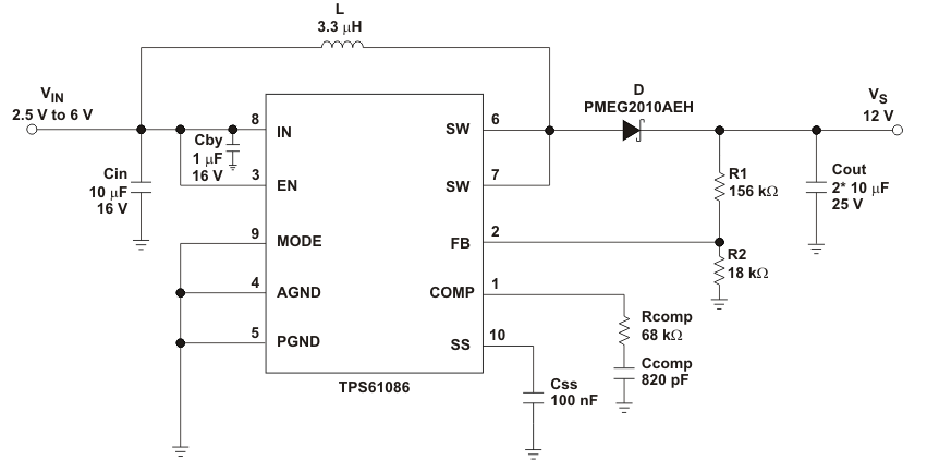
Simplified Schematic
TPS61086 appa_sch_lvsa05.gif