SLVS658C March 2006 – January 2016 TPS65810 , TPS65811
PRODUCTION DATA.
- 1 Features
- 2 Applications
- 3 Description
- 4 Revision History
- 5 Description (continued)
- 6 Pin Configuration and Functions
-
7 Specifications
- 7.1 Absolute Maximum Ratings
- 7.2 ESD Ratings
- 7.3 Recommended Operating Conditions
- 7.4 Thermal Information
- 7.5 Electrical Characteristics - System Sequencing and Operating Modes
- 7.6 Electrical Characteristics - Power Path and Charge Management
- 7.7 Electrical Characteristics - Power Path and Charge Management (Continued)
- 7.8 Electrical Characteristics - Power Path and Charge Management (Continued)
- 7.9 Electrical Characteristics - Linear Regulators
- 7.10 Electrical Characteristics - Switched-Mode SM1 Step-Down Converter
- 7.11 Electrical Characteristics - Switched-Mode SM2 Step-Down Converter
- 7.12 Electrical Characteristics - GPIOs
- 7.13 Electrical Characteristics - ADC
- 7.14 Electrical Characteristics - LED and PWM Drivers
- 7.15 Electrical Characteristics - I2C Interface
- 7.16 Timing Requirements - I2C Interface
- 7.17 Trigger Timing Characteristics
- 7.18 Dissipation Ratings
- 7.19 Typical Characteristics
-
8 Detailed Description
- 8.1 Overview
- 8.2 Functional Block Diagram
- 8.3
Feature Description
- 8.3.1 Interrupt Controller and System Sequencing
- 8.3.2
Power Path and Charge Management
- 8.3.2.1 Overview
- 8.3.2.2
Power Path Management Function
- 8.3.2.2.1 Detecting the System Status
- 8.3.2.2.2 Power Path Logic: Priority Algorithm
- 8.3.2.2.3 Input Current Limit
- 8.3.2.2.4 System Voltage Regulation
- 8.3.2.2.5 Input Overvoltage Detection
- 8.3.2.2.6 Output Short-Circuit Detection
- 8.3.2.2.7 Battery Short-Circuit Detection
- 8.3.2.2.8 Initial Power Path Operation
- 8.3.2.2.9 No-Battery Detection Circuit
- 8.3.2.2.10 Using the Input Power to Run the System and Charge the Battery Pack
- 8.3.2.3
Battery Charge Management Function
- 8.3.2.3.1 Operating Modes
- 8.3.2.3.2 Battery Preconditioning
- 8.3.2.3.3 Constant Current Charging
- 8.3.2.3.4 Charge Termination and Recharge
- 8.3.2.3.5 Battery Voltage Regulation, Charge Voltage
- 8.3.2.3.6 Temperature Qualification
- 8.3.2.3.7 Dynamic Power Path Management
- 8.3.2.3.8 Charger Off Mode
- 8.3.2.3.9 Precharge Safety Timer
- 8.3.2.3.10 Charge Safety Timer
- 8.3.2.3.11 Timer Fault Recovery
- 8.3.2.3.12 Dynamic Timer Function
- 8.3.2.4 Functionality Guide — System Power and Charge Management
- 8.3.3 Linear Regulators
- 8.3.4
Step-Down Switched-Mode Converters: SM1 and SM2
- 8.3.4.1 Output Voltage Slew Rate
- 8.3.4.2 Soft-Start
- 8.3.4.3 Dropout Operation at 100% Duty Cycle
- 8.3.4.4 Output Voltage Monitoring
- 8.3.4.5 Stand-by Mode
- 8.3.4.6 PWM Operation
- 8.3.4.7 Phase Control in PWM Mode
- 8.3.4.8 PFM Mode Operation
- 8.3.4.9 Functionality Guide — Switched-Mode Step-Down Converters
- 8.3.5
Analog-to-Digital Converter
- 8.3.5.1 Overview
- 8.3.5.2 Input Channels
- 8.3.5.3
Functional Overview
- 8.3.5.3.1 ADC Conversion Cycle
- 8.3.5.3.2 External Trigger Operation
- 8.3.5.3.3 Detecting an External Trigger Event
- 8.3.5.3.4 Executing Multiple-Sample Cycles With an External Trigger
- 8.3.5.3.5 Continuous Conversion Operation (Repeat Mode)
- 8.3.5.3.6 ADC Input Signal Range Setting
- 8.3.5.3.7 ADC State Machine
- 8.3.5.4 Battery Detection Circuit
- 8.3.5.5 Functionality Guide - Analog to Digital Converter
- 8.3.6 LED and Peripheral Drivers
- 8.3.7 General-Purpose I/Os — GPIO 1, 2, 3
- 8.4 Device Functional Modes
- 8.5
Programming
- 8.5.1
Serial Interface
- 8.5.1.1 Overview
- 8.5.1.2 Register Default Values
- 8.5.1.3 I2C Address
- 8.5.1.4 Incremental Read
- 8.5.1.5 I2C Bus Release
- 8.5.1.6 Sleep Mode Operation
- 8.5.1.7 I2C Communication Protocol
- 8.5.1.8 I2C Read and Write Operations
- 8.5.1.9 Valid Write Sequences
- 8.5.1.10 One-Byte Write
- 8.5.1.11 Valid Read Sequences
- 8.5.1.12 Non-Valid Sequences
- 8.5.1
Serial Interface
- 8.6
Register Maps
- 8.6.1 Sequencing and Operating Modes - I2C Registers
- 8.6.2 System Status — I2C Registers
- 8.6.3 Interrupt Controller - I2C Registers
- 8.6.4 Charge and System Power Management — I2C Registers
- 8.6.5 Linear Regulators — I2C Registers
- 8.6.6 Switched-Mode Step-Down Converters — I2C Registers
- 8.6.7 ADC - I2C Registers
- 8.6.8 White LED, PWM Drivers — I2C Registers
- 8.6.9 GPIOs — I2C Registers
- 9 Application and Implementation
- 10Power Supply Recommendations
- 11Layout
- 12Device and Documentation Support
- 13Mechanical, Packaging, and Orderable Information
8 Detailed Description
8.1 Overview
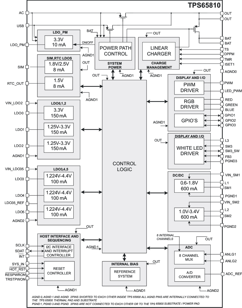
This power management IC (PMIC) integrates a battery charger, nine LDOs, two buck converters, a white LED driver, and an RGB driver in a 56-pin QFN package.
8.2 Functional Block Diagram
8.3 Feature Description
8.3.1 Interrupt Controller and System Sequencing
8.3.1.1 Overview
The TPS65810 has two dedicated internal controllers that execute the host interface and system sequencing tasks: a sequencing controller and an interrupt controller.
The sequencing controller monitors internal and system parameters and defines the sequencing of the internal power supplies during power-up, power-down, or power fault events, and executes specific internal power supply reset operations under external hardware control or host software commands.
The following parameters are monitored by the sequencing controller:
- System power bus voltage (at SYS_IN pin), input supply voltage, battery pack voltage
- TPS65810 thermal fault status
- Integrated supply status
The interrupt controller monitors multiple system status parameters and signals to the host when one of the monitored parameters toggled, as a result of a system status change. The interrupt controller inputs include all the parameters monitored by the sequencing controller plus:
- Charger status
- Battery pack status
- ADC status
Internal I2C registers enable masking of all the monitored parameters. Using those registers, the host can select which parameters trigger an interrupt or a power-good fault. Power-good faults trigger a change in the TPS65810 operating mode, as detailed in the next sections.
Figure 16 shows a simplified block diagram for the TPS65810 sections that interface to the external host.
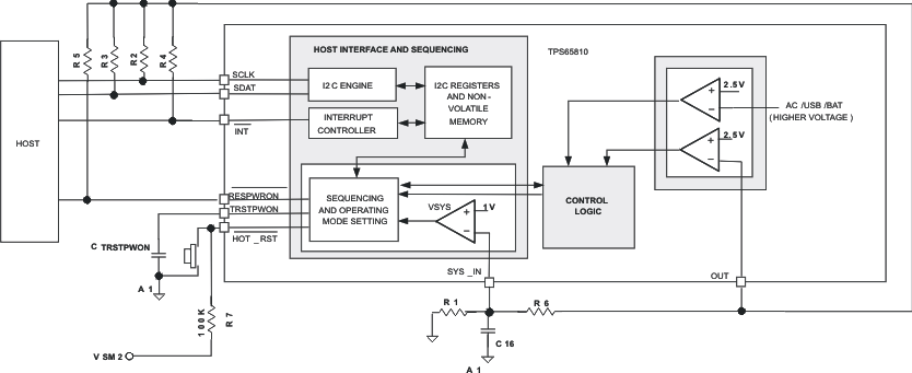 Figure 16. Simplified Block Diagram
8.3.1.2 Interrupt Controller
The TPS65810 has internal block and overall system status information stored in I2C status registers. The following subsystems and system parameters are monitored:
- External power supply status: AC or USB supply detected, AC or USB connected to system, AC/USB OVP
- Charger status: on, off, or suspend, fast charge or precharge, termination detected, DPPM on, thermal loop ON
- Battery pack status: temperature, discharge on and off
- TPS65810 thermal shutdown
- ADC status: conversion status, input out of range, ANLG1 high impedance detection
- Integrated supplies status: output out of regulation (power-good fault)
The GPIO1 and GPIO2 pins can be configured as inputs, generating an interrupt request to the host (INT:HI→LO) at the GPIO rising or falling edge. The host can use internal the INT_MASK I2C registers to define which of the monitored status variables triggers an interrupt. When a non-masked system status bit toggles state, the interrupt controller issues an interrupt, following the steps below:
- System status bits that caused the interruption are set to HI in registers INT_ACK1 and INT_ACK2
- An interrupt is sent to the host (INT:HI→LO)
When an interrupt is sent to the host, INT is kept in the LO state and the INT_ACK register contents are latched, holding the system status that generated the currently issued interrupt request. When an interrupt request is active (INT = LO) additional changes in non-masked status registers and control signals are ignored, and the INT_ACK registers are not updated.
The host must write a 0 to the INT_ACK register bit that generated the interrupt to set INT = HI and enable new updates to the INT_ACK registers. If the host stops in the middle of a WRITE or READ operation, the INT pin stays at the LO level. The TPS65810 has no reset timeout; assume that the host does not leave INT = LO and the status registers unread for a long time.
The non-masked I2C register bits and internal control signals generate a new interrupt only after INT is set to HI. The non-masked power-good fault register bits generate a power-good fault when any of the non-masked bits detects that the monitored output voltage is out of regulation, independently of the INT pin level.
8.3.1.3 System Sequencing and TPS65810 Operating Modes
The TPS65810 has a state machine that controls the device power-up and power-down sequencing. Figure 17 is a state diagram which shows the main operating modes.
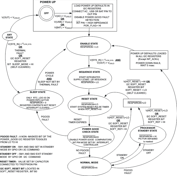 Figure 17. TPS65810 State Diagram
8.3.1.3.1 Power Up
If the AC, USB and BAT pin voltages are below the internal UVLO threshold VUVLO (2.5 V typical) all IC blocks are disabled and the TPS65810 is not operational, with all functions OFF. When an external power source or battery with voltage greater than the VUVLO voltage threshold is applied to AC/USB or BAT pins the internal TPS65810 references are powered up, biasing internal circuits. When all the main internal supply rails are active the TPS65810 I2C registers are set to the power-up default values, shown in Table 1.
Table 1. Integrated Supply and Drivers I2C Registers Power-Up Defaults
| SUPPLY | POWER-UP DEFAULT | OTHER BLOCKS | POWER-UP DEFAULT |
|---|---|---|---|
| LDO0 | OFF, 3.3 V | POWER PATH | INPUT TO SYSTEM |
| LDO1 | 1.25V, OFF | PWM | OFF |
| LDO2 | 3.3 V, OFF | PWM_LED | OFF |
| LDO3 | 1.505 V, OFF | GPIO1 | INPUT, SM1 ON/OFF CONTROL |
| LDO4 | 1.811 V, OFF | GPIO2 | INPUT, SM2 ON/OFF CONTROL |
| LD05 | 3.111 V, ON | GPIO3 | INPUT |
| SIM | 2.5 V, ON | ADC | OFF |
| RTC_OUT | ON, 1.5 V | SM3 (WHITE LED) | OFF |
| LDO_PM | 3.3 V, ON at OUT POWERED | RGB DRIVER | OFF |
| SM1 | OFF, 1.24 V | INTERRUPT MASK | NONE MASKED |
| SM2 | OFF, 3.32 V | POWER-GOOD MASK | ALL MASKED |
| CHARGER | OFF |
After the internal I2C register power-up defaults are loaded the power path control logic is enabled, connecting the external power source to the OUT pin. A status flag (nRAMLOAD) is set to LO in the SOFT_RESET register, indicating that the I2C registers were loaded with the power-up defaults, and the TPS65810 enters the ENABLE state.
8.3.1.3.2 Enable
In the ENABLE mode the RESPWRON output is set to the LO level, the INT pin mode is set to high impedance and all the power-good comparators that monitor the integrated supply outputs are disabled. The ENABLE mode is used by the TPS65810 to detect when the main system power rail (OUT pin) is powered and ready to be used on the internal supply power-up. The OUT pin voltage is sensed by an internal low-system-voltage comparator which holds the IC in the ENABLE mode until the system power-bus voltage (OUT pin) has reached a minimum operating voltage, defined by the user. The internal comparator senses the system voltage at pin SYS_IN, and the threshold for the minimum system operating voltage at the OUT pin is set by the external divider connected from OUT pin to SYS_IN pin. The threshold voltage is calculated in Equation 1.

where
- R6 and R1 are external resistors
- V(LOW_SYS) = 1 V (typical)
The minimum system operating voltage must always be set above the internal UVLO threshold VUVLO. In normal application conditions the minimum system operating voltage is usually set to a value that assures that the TPS65810 integrated regulators are not operating in the dropout region.
When the voltage at the SYS_IN pin exceeds the internal threshold V(LOW_SYS) the TPS65810 device is ready to start the system power sequencing, and the SEQUENCING mode is entered.
8.3.1.3.3 Sequencing
The sequencing state starts immediately after the enable state. In this mode of operation the integrated supplies are turned ON. The TPS65810 sequencing timing diagram shown in Figure 18 details the internal timing delays and supply sequencing. At the end of the sequencing state the user-programmable reset timer is started, and the TPS65810 enters the reset state.
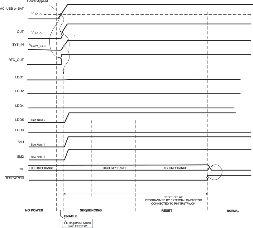
8.3.1.3.4 Reset
When the reset state starts the RESPWRON output is LO. The user can program the reset timer value by selecting the value of the external capacitor connected to pin TRSTPWON, as shown in Equation 2.
where
- KRESET is the reset timer constant (1 ms/nF typical)
The TPS65810 RESPWRON pin must be used to reset the external host. During the external host reset (RESPWRON = LO) the I2C SDA and SCL pins are not used to access TPS65810 internal registers. If a non-standard configuration is used to reset the system the SDA and SCL lines must not be used to communicate with the TPS65810 until RESPWRON = HI, to avoid overwriting the integrated power supply internal power-up settings during the sequencing mode.
The power-good comparators are masked during the reset mode. The reset mode ends when the reset timer expires, and the TPS65810 goes into the power-good check mode.
The RESPWRON signal set to a high level is the proper signal to use as an indicator that the device has transitioned out of the reset state. During the power-up sequence the RESPWRON pin is asserted LOW until the RESET TIMER expires. The RESET TIME (treset = 1ms/nF × CTRSTPWON) can be programmed through a capacitor between the TRSTPWON pin and ground.
When the RESPWRON signal is LO, all internal and external interrupts are ignored. As a result, the open-drain output that asserts the INT pin LO during a NORMAL MODE interrupt request is disabled. The INT pin is then asserted HI through a pullup resistor that is typically connected to VOUT. After the RESPWRON signal goes HI, the interrupt controller is given control of the INT pin. Finally, the rising edge of the RESPWRON pin must be used to indicate the PMIC has transitioned from the RESET STATE to the POWER-GOOD CHECK STATE. At that point, the interrupt controller asserts an interrupt if necessary.
8.3.1.3.5 Power-Good Check
In the power-good check mode the power-good comparators are enabled, providing status on the integrated supplies output voltages. An output voltage is considered as out of regulation and generates a fault condition if the output voltage is below 90% of the target output voltage regulation value. If a power-good fault is detected the SLEEP mode is set, if a power-good fault is not detected the NORMAL mode is set.
The individual supply power-good status can be masked through an I2C register PGOODFAULT_MASK. Supplies that have their power-good fault status masked do not generate a power-good fault. However, the status bit for the supply indicates that the output voltage is out of regulation.
The power-good mask register bits default to masked upon power up.
8.3.1.3.6 Sleep Mode
The SLEEP mode is set when a thermal fault or system low voltage fault is detected, under NORMAL operation mode set. This operation mode is also set when a power-good fault is detected during the power-good check state or the I2C bit SLEEP_MODE. In the SLEEP mode the RESPWRON output is set to LO, and the I2C registers keep the same contents as in the state preceding SLEEP mode, with the exception of the following control bits, which are reset to the default power-up values:
- LDO1,2,3,4,5 and RTC_OUT are enabled, SIM LDO is disabled: EN_LDO register set to default values
- LDO0 disabled, all GPIOs with no control function assigned: GPIO12, GPIO3 registers set to default values
- White LED driver is set to OFF: SM3_SET register has all bits set to LO
- RGB drivers are set to OFF: RGB_FLASH, RGB_RED, RGB_GREEN, RGB_BLUE registers are set to default values
- PWM, PWM_LED drivers OFF: PWM, LED_PWM registers are set to default values
- ADC engine reset to power-up default: ADC_SET, ADC_DELAY, ADC_WAIT registers are set to default values
NOTE
In SLEEP mode the power path and main internal blocks are still active, but the internal integrated supply sequencing is disabled. As a result of that, during SLEEP mode ALL integrated supplies (ALL LDO's, ALL buck Converters) are disabled.
At the end of the SLEEP mode, the sequencer block uses the I2C control register values (which were reset to the default power-up values) to sequence the integrated power supplies. The SLEEP mode ends when one of the three following events occurs:
- If SLEEP was set by thermal fault: The SLEEP mode ends only when all external input supplies and battery pack are removed and a UVLO condition is detected by the TPS65810, setting the NO POWER mode.
- If SLEEP was set by a system low voltage detection, or I2C bit SLEEP_MODE, only with battery present: Input power must be connected, setting the TPS65810 in the ENABLE mode. If no input power is inserted, the battery discharges until the TPS65810 detects a UVLO condition and enters the NO POWER mode.
- If sleep was set by a system low voltage detection, power-good fault or SLEEP_MODE, with battery and input power present: all external input supplies connected to AC and USB pins must be removed, and then at least one of them reconnected to the system. The input power cycling triggers a transition from SLEEP mode to the ENABLE mode.
8.3.1.3.7 Normal Mode
If a power-good fault is not present at the end of the power-good check mode the NORMAL mode starts. In this mode of operation the I2C registers define the TPS65810 operation, and the host has full control on operation modes, parameter settings, and so forth. The normal state operation ends if a thermal fault, system low voltage fault (V(SYS_IN) < VLOW_SYS) or power-good fault is detected. A thermal fault or system low voltage fault sets the SLEEP mode operation, a power-good fault sets the NO POWER operation mode. From the normal mode the converters SM1 and SM2 can be set in the STANDBY mode, with reduced output voltages. In NORMAL mode either an I2C register bit (SOFT_RESET register bit SOFT_RST) or a hardware input ( HOT_RESET pin set to LO) can trigger a transition to the RESET state, enabling implementation of a host reset function. In NORMAL mode an I2C register bit (SOFT_RESET register bit SLEEP_MODE) can trigger a transition to SLEEP mode.
8.3.1.3.8 Processor Standby State
This state is set using an I2C register or a GPIO configured as SM1 and SM2 stand-by control. In stand-by mode operation, the SM1 and SM2 voltages are set to value distinct than the normal mode output voltage, and SM1/SM2 are set to PFM mode. The stand-by output voltage is defined in I2C registers SM1_STANDBY and SM2_STANDBY.
8.3.1.4 TPS65810 Operating Mode Controls
The three operating mode controls are defined as follows:
-
HARDWARE RESET A dedicated control pin, HOT_RESET, enables implementation of a hardware reset function. The system reset pin RESPWRON is set to LO when HOT_RESET = LO for a period longer than the internal deglitch (5 ms typical). The RESET mode is started when the HOT_RESET pin transitions from LO to HI, as shown in the state diagram. When HOT_RESET = LO all I2C registers are reset to the default power-up values.
-
SOFTWARE RESET The external host can set the TPS65810 device in RESET mode using the I2C register SOFT_RESET, bit B0 (SOFT_RST).
-
SOFTWARE SLEEP The external host can set the TPS65810 in SLEEP mode using the I2C register SOFT_RESET, bit B6 (SLEEP_MODE).
A software reset does not affect the contents of the I2C registers.
8.3.1.5 Functionality Reference Guide – Host Interface and System Sequencing
Table 2. Interrupt Controller, Open-Drain Output (INT)
| SYSTEM PARAMETERS MONITORED BY THE INTERRUPT CONTROLLER | POWER UP DEFAULT |
||||
|---|---|---|---|---|---|
| SUPPLY OUTPUT POWER-GOOD FAULT DETECTION(1) |
SYSTEM STATUS MODIFICATION |
ADC STATUS | CHARGER STATUS TRANSITION | INPUT AND OUTPUT POWER TRANSITION |
|
| SM1, SM2, SM3, LDO1, LDO2, LDO3, LDO4, LDO5 |
Thermal Fault or GPIO 1,2 configured as external interrupt request | ADC conversion end ADC Input out of range External resistive load connected to ANLG1 |
Charge: Pre↔ Fast ↔Done DPPM:on ↔ off Charge Suspend: on ↔ off Thermal Foldback: on ↔ off |
AC detected: yes ↔ no USB detected: yes ↔ no Input OVP: yes ↔ no System Power: AC ↔ USB |
All interrupt controller inputs set to non-masked |
| Can be masked Individually through I2C. Blanked during initial power up | Can be masked Individually through I2C | Can be masked as a group through a single I2C mask register bit | |||
Table 3. Events Triggering TPS65810 Operating Mode Changes
| EVENT | POWER-GOOD FAULT DETECTION(1) | THERMAL FAULT | HARDWARE RESET | SOFTWARE RESET |
|---|---|---|---|---|
| How transition is triggered | Integrated regulator output voltage below target value: SM1, SM2, SM3, LDO1, LDO2,LDO3, LDO4, LDO5 | Internal IC junction temperature | Using HOT_RST control pin | I2C register control bit |
| Operating mode change | Sets Sleep mode or starts a new power-up cycle when power-good fault is detected (see state machine diagram). | Sets Sleep mode when thermal fault is detected | Generates external host reset pulse at pin RESPWON when HOT_RST = LO. | Generates external host reset pulse at pin RESPWON when I2C control bit is set. |
| Power-good fault detection comparators are blanked during initial power-up. | Input and Battery power cycling required to exit sleep | Pulse duration set by external capacitor. | Pulse duration set by external capacitor. | |
| Controls | Can be masked Individually through I2C. | Fixed Internal Threshold | External Input | Set through I2C |
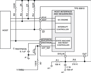 Figure 19. Required External Components, Recommended Values, External Connections
8.3.2 Power Path and Charge Management
8.3.2.1 Overview
The TPS65810 has an integrated charger with power path integrated MOSFETs. This topology, shown in Figure 20, enables using an external input power to run the system and charge the battery simultaneously. The power path has dual inputs that can be used to select either an external AC_DC adapter (AC pin) or an USB port power (USB pin) to power the end equipment main power rail (OUT pin, also referred to as the system power bus) and charge the battery pack (connected to BAT pin).
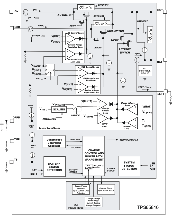 Figure 20. TPS65810 Charger and Power Path Section Simplified Block Diagram
The power path has three integrated power MOSFETs: the battery to system MOSFET (battery switch), the AC input to system MOSFET (AC switch) and the USB input to system MOSFET (USB switch). Each of those power MOSFETs can be operated either as an ON/OFF switch or as a linear pass element under distinct operating conditions, as defined by the control circuits that set the power MOSFET gate voltage.
The TPS65810 regulates the voltage at the OUT pin to 4.6 V when one of the external supplies connected to pins AC or USB is powering the OUT pin. The selected input (AC or USB pin) current is limited to a value defined by I2C register settings. The input current limit function assures compatibility with USB standard requirements, and also implements a protection function by limiting the maximum current supplied by an external AC_DC adapter or USB port power terminal.
The AC power MOSFET and USB power MOSFET operating modes are set by integrated control loops. Each of the power MOSFETs is controlled by two loops: one system voltage regulation loop and one input current limiting loop. The integrated loops modulate the AC or USB power MOSFETs drain to source resistance to regulate either the OUT pin voltage or to limit the input current. If no input power is present (AC and USB input power not detected) the AC and USB power MOSFETs are turned OFF, and the battery MOSFET is turned ON, connecting the BAT pin to the OUT pin.
The battery switch is turned ON when the AC or USB input power is detected and the charger function is enabled, charging the battery pack. During charge the battery MOSFET switch operation mode is defined by the charger control loops. The battery MOSFET switch drain-to-source resistance is modulated by the charge current loop and charge voltage loop to implement the battery charging algorithm. In addition to that multiple safety functions are activated (thermal shutdown, safety timers, short-circuit recovery), and additional functions (thermal loop and DPPM loop) optimize the charging process.
8.3.2.2 Power Path Management Function
8.3.2.2.1 Detecting the System Status
The power path and charge management block operate independently of the other TPS65810 circuits. Internal circuits check battery parameters (pack temperature, battery voltage, charge current) and system parameters (AC and USB voltage, battery voltage detection), setting the power path MOSFETs operating modes automatically. The TPS65810 has integrated comparators that monitor the battery voltage, AC pin voltage, USB pin voltage and the OUT pin voltage. The data generated by those comparators is used by the power path control logic to define which of the integrated power path switches are active. Figure 21 shows a simplified block diagram for the system status detection.
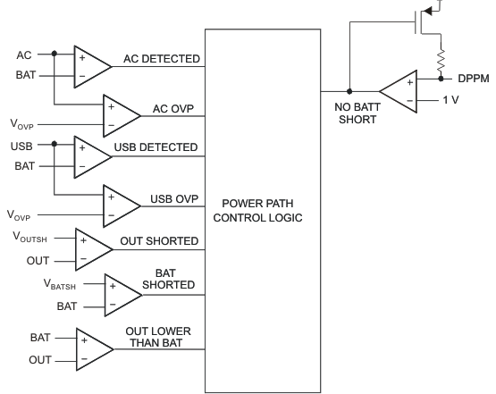 Figure 21. TPS65810 Systems Status Detection, Charger and Power Path Section
Table 4 lists the system power detection conditions. VIN(DT), VOUTSH, VBATSH, VOVP are the TPS65810 internal references, refer to the electrical characteristics in the Specifications section for additional details.
Table 4. System Status Detection, Charger and Power Path Section
| SYSTEM STATUS DETECTION | CONDITION |
|---|---|
| AC input voltage detected | V(AC) – V(BAT) > VIN(DT) |
| USB input voltage detected | V(USB) – V(BAT) > VIN(DT) |
| AC overvoltage detected | V(AC) > VOVP |
| USB overvoltage detected | V(USB) > VOVP |
| AC PIN TO OUT pin OR USB TO OUT PIN short detected | V(OUT) < VINOUTSH |
| BAT pin to OUT pin short detected | V(BAT) - V(OUT) > VBATOUTSH |
| Battery supplement mode need detected | V(BAT) – V(OUT) > VSUP |
| Blank BAT to OUT short circuit detection | V(DPPM) < 1V |
8.3.2.2.2 Power Path Logic: Priority Algorithm
The system power bus supply is automatically selected by the power path control logic, following an internal algorithm. The power path function detects an external input power connection when the input voltage exceeds the battery pack voltage. It also detects a supplement mode need (battery switch must be turned ON) when the system voltage (OUT pin) is below the battery voltage. A connected and non-selected external supply or the battery is automatically switched to the system bus, following the priority algorithm, when the external supply currently selected is disconnected from the system.
The input power priority is hard-wired internally, with the AC input having the higher priority, followed by the USB input (2nd) and the battery pack (3rd). Using the I2C CHG_CONFIG register control bit CE the user can override the power path algorithm, connecting the battery to the system power bus. Take care when using the battery-to-system connection option, as the system power bus is not connected back to the AC or USB inputs (even if those are detected) when the battery is removed. Table 5 describes the priority algorithm.
Table 5. Power Path Control Logic Priority Algorithm
| CE BIT (I2C CHG_CONFIG Register) |
EXTERNAL SUPPLY DETECTED | SWITCH MODE | SYSTEM POWER SOURCE |
|||
|---|---|---|---|---|---|---|
| AC | USB | AC | USB | BATTERY | ||
| HI | YES | NO | ON | OFF | ON if Supplement mode is required, OFF otherwise | AC |
| NO | YES | OFF | ON | USB | ||
| YES | YES | ON | OFF | AC | ||
| NO | NO | OFF | OFF | BATTERY | ||
| LO | XX | XX | OFF | OFF | ON | BATTERY |
The power path status is stored in register CHG_STAT.
8.3.2.2.3 Input Current Limit
The USB input current is limited to the maximum value programmed by the host, using the I2C interface. If the system current requirements exceed the input current limit, the output voltage collapses, the charge current is reduced, and finally, the supplement mode is set. The input current limit value is set with the I2C charge control register bits PSEL and ISET2, and it is applied to the USB input ONLY. The AC input current limit is fixed to the internal short circuit limit value.
Table 6. Charge-Current Scaling Through I2C
| PSEL (I2C) | ISET2 (I2C) | INPUT CURRENT LIMIT | |
|---|---|---|---|
| USB | AC | ||
| LO | LO | 100 mA | 2.75 A |
| LO | HI | 500 mA | 2.75 A |
| HI | LO | 2.75 A | 2.75 A |
| HI | HI | 2.75 A | 2.75 A |
8.3.2.2.4 System Voltage Regulation
The system voltage is regulated to a fixed voltage when one of the input power supplies is connected to the system. The system voltage regulation is implemented by a control loop that modulates the selected switch Rds(on).
The typical system regulation voltage is 4.6 V.
8.3.2.2.5 Input Overvoltage Detection
The AC and USB input voltages are monitored by voltage comparators that identify an overvoltage condition. If an overvoltage condition is detected a status register bit is set, indicating a potential fault condition.
When an overvoltage condition is detected, the AC or USB switches state is not modified. If any of those switches was ON, it is kept in the ON state. During overvoltage conditions, the system voltage is still regulated, and no major safety issues are observed when not modifying the input switch state.
If the input overvoltage condition results in excessive power dissipation, the thermal shutdown circuit is activated, the AC and USB switches are turned OFF, and the BAT switch is turned ON.
8.3.2.2.6 Output Short-Circuit Detection
If the OUT pin voltage falls below an internal threshold VINOUTSH the AC and USB switches are turned off and internal pullup resistors are connected from AC pin to OUT pin and USB pin to OUT pin. When the short circuit is removed those resistors enable the OUT pin voltage to rise above the VINOUTSH threshold, returning the system to normal operation.
8.3.2.2.7 Battery Short-Circuit Detection
If the OUT pin voltage falls below the BAT pin voltage by more than an internal threshold VBATOUTSH the battery switch is turned off and internal pullup resistor is connected between the OUT pin and the BAT pin. This resistor enables detection of the short removal, returning the system to normal operation.
8.3.2.2.8 Initial Power Path Operation
During the initial TPS65810 power-up the contents of the ISET2, CE and SUSPEND bits on the control register are immediately implemented. The charger is disabled (SUSPEND=LO) and the selected input current limit is set internally to 500 mA max.
8.3.2.2.9 No-Battery Detection Circuit
The ANLG1 pin may be used to detect the connection of an external resistor that is embedded in a battery pack and is used as a pack ID function. The ANLG1 pin has an internal current source connected between OUT and ANLG1, which is automatically enabled when the TPS65810 is not in SLEEP mode. The current levels for ANLG1 pin can be programmed through I2C register ADC_WAIT, bits BATID_n, as shown in Figure 22.
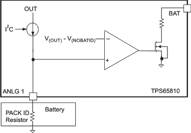 Figure 22. Battery Removal Detection, ANLG1 Pin
An internal comparator with a fixed deglitch time, t DGL(NOBAT) monitors the ANLG1 pin voltage, if V(ANLG1) > V(OUT) – VNOBATID, a battery removed condition is detected and an internal discharge switch is activated, connecting an internal resistor from BAT pin to AGND1. Note that ANLG1 can also be used as an analog input for the ADC converter, in this case the voltage at pin ANLG1 must never exceed the V(OUT) – VNOBATID, threshold to avoid undesired battery discharge.
8.3.2.2.10 Using the Input Power to Run the System and Charge the Battery Pack
The external supply connected to AC or USB pins must be capable of supplying the system power and the charger current. If the external supply power is not sufficient to run the system and charge the battery pack the TPS65810 executes a two-stage algorithm that prevents a low voltage condition at the system power bus:
- The charge current is reduced, until the total (charger + system current) is at a level that can be supplied by the external input supply. This function is implemented by a dedicated charger control loop (see Dynamic Power Path Management for additional details).
- The battery switch is turned ON if the charge current is reduced to zero and the input current is not enough to run the system. In this mode of operation both the battery and the external input power supply the system power ( supplement operation mode).
The supplement operation mode is automatically set by the TPS65810 when the input power is switched to the OUT pin, and the OUT pin voltage falls below the battery voltage.
8.3.2.3 Battery Charge Management Function
8.3.2.3.1 Operating Modes
The TPS65810 supports charging of single-cell Li-Ion or Li-Pol battery packs. The charge process is executed in three phases: precharge (or preconditioning), constant current and constant voltage.
The charge parameters are selectable through I2C interface and using external components. The charge process starts when an external input power is connected to the system, the charger is enabled by the I2C register CHG_CONFIG bits CE = HI and CHGON = HI, and the battery voltage is below the recharge threshold, V(BAT) < V(RCH). When the charge cycle starts a safety timer is activated. The safety timer timeout value is set by an external resistor connected to the TMR pin.
When the charger is enabled two control loops modulate the battery switch drain to source impedance to limit the BAT pin current to the programmed charge current value (charge current loop) or to regulate the BAT pin voltage to the programmed charge voltage value (charge voltage loop). If V(BAT) < 3 V (typical) the BAT pin current is internally set to 10% of the programmed charge current value. Figure 23 shows a typical charge profile for an operation condition that does not cause the IC junction temperature to exceed 125°C (typical).
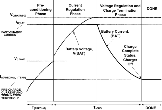 Figure 23. Typical Charge Cycle, Thermal Loop not Active
If the operating conditions cause the IC junction temperature to exceed 125°C the charge cycle is modified, with the activation of the integrated thermal control loop. The thermal control loop is activated when an internal voltage reference, which is inversely proportional to the IC junction temperature, is lower than a fixed, temperature stable internal voltage. The thermal loop overrides the other charger control loops and reduces the charge current until the IC junction temperature returns to 125°C, effectively regulating the IC junction temperature.
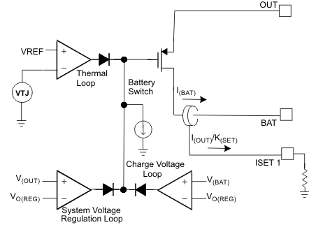
Figure 24 shows a modified charge cycle, with the thermal loop active.
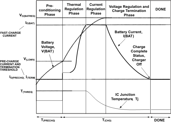 Figure 24. Typical Charge Cycle, Thermal Loop Active
8.3.2.3.2 Battery Preconditioning
The TPS65810 applies a precharge current Io(PRECHG) to the battery if the battery voltage is below the V(LOWV) threshold, preconditioning deeply discharged cells. The charge current loop regulates the ISET1 pin voltage to an internal reference value, V(PRECHG). The resistor connected between the ISET1 and AGND pins, RSET, determines the precharge rate.
The precharge rate programmed by RSET is always applied to a deeply discharged battery pack, independently of the input power selection (AC or USB). Use Equation 3 to calculate the precharge current.

where
- K(SET) is the charge current scaling factor
- V(PRECHG) is the precharge set voltage
8.3.2.3.3 Constant Current Charging
The constant charge current mode (fast charge) is set when the battery voltage is higher than the precharge voltage threshold. The charge current loop regulates the ISET1 pin voltage to an internal reference value, VSET. The fast charge current regulation point is defined by the external resistor connected to the ISET1 pin, RSET, as shown in the following:

where
- V(SET) (2.5 V typical) is the voltage at ISET1 pin during charge current regulation
- K(SET) = charge- current scaling factor
The reference voltage V(SET) can be reduced through I2C register CHG_CONFIG bits ISET1_1 and ISET1_0. V(SET) can be selected as a percentage (75%, 50% or 25%) of the original 2.5 V typ, non-attenuated V(SET) value, effectively scaling down the charge current.
The ISET1 resistor always sets the maximum charge current if the AC input is selected. When the USB input is selected, the maximum charge current is defined by the USB input current limit and the programmed charge current. If the USB input current limit is lower than the IO(OUT) value, the battery switch is set in the dropout region and the charge current is defined by the input current limit value and system load, as shown in Figure 25.
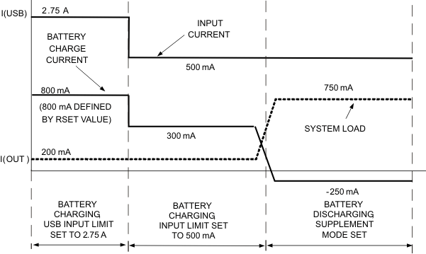 Figure 25. Input Current Limit Impact on Effective Charge Current
8.3.2.3.4 Charge Termination and Recharge
The TPS65810 monitors the charging current during the voltage regulation phase. Charge is terminated when the charge current is lower than an internal threshold, set to 10% (typical) of the fast charge current rate. The termination point applies to both AC and USB charging. Use Equation 5 to calculate the termination point, I(TERM).

where
- V(TERM) is the termination detection voltage reference
The voltage at ISET1 pin is monitored to detect termination, and termination is detected when V(SET1) < V(TERM) (0.25 V typical). The voltage reference V(TERM) is internally set to 10% of the V(SET) reference voltage, and it is modified if the reference voltage V(SET) is scaled through I2C register CHG_CONFIG bits ISET1_1 and ISET1_0. V(TERM) is reduced by the same percentage used to scale down V(SET).
Table 7 lists the charge current and termination thresholds for a 1-A charge current set (1-kΩ resistor connected to ISET1 pin), with the selected input current limit set to a value higher than the programmed charge current. The termination current is scaled for all charge current modes (AC or USB), as it is always set by the ISET1 pin external resistor value.
Table 7. Charge Current and Termination Threshold Selection Example
| CHARGE CONTROL REGISTER BITS | CHARGE CURRENT, (% OF TYPICAL VALUE PROGRAMMED BY ISET1 RESISTOR) | V(SET) (V) | V(TERM) (mV) | CHARGE CURRENT (A) | TERMINATION CURRENT (mA) | |
|---|---|---|---|---|---|---|
| ISET1_1 | ISET1_0 | |||||
| 0 | 0 | 25% | 0.6 | 60 | 0.24 | 20 |
| 0 | 1 | 50% | 1.25 | 115 | 0.5 | 40 |
| 1 | 0 | 75% | 1.9 | 160 | 0.78 | 60 |
| 1 | 1 | 100% | 2.5 | 250 | 1 | 100 |
When the termination is detected, a new charge cycle starts if the voltage on the BAT pin falls below the V(RCH) threshold. A new charge start is also triggered if the charger is enabled, disabled, or re-enabled through I2C (CHG_CONFIG register bits CE or CHGON), or if both AC and USB input power are removed and then at least one of them is re-inserted.
The termination is disabled when the thermal loop OR DPPM loop are active, and during supplement mode.
8.3.2.3.5 Battery Voltage Regulation, Charge Voltage
The voltage regulation feedback is Implemented by sensing the BAT pin voltage, which is connected to the positive side of the battery pack. The TPS65810 monitors the battery-pack voltage between the BAT and AGND1 pins, when the battery voltage rises to the VO(REG) threshold the voltage regulation phase begins and the charging current tapers down.
The charging voltage can be selected as 4.2 V or 4.365 V (typical). The default power-up voltage is 4.2 V. As a safety measure the 4.365 V charge voltage is programmed only if two distinct bits are set through I2C: VCHG=HI in the CHG_CONFIG, and CHG_VLTG=LO in the GPIO3 register.
8.3.2.3.6 Temperature Qualification
The TPS65810 charger section does not monitor the battery temperature. This function may be implemented by an external host, which can measure the pack temperature by monitoring the ADC channel connected to the TS pin. An external pullup resistor must be connected to the TS pin to bias the pack thermistor, as the TPS65810 device has no internal current source connected to the TS pin.
8.3.2.3.7 Dynamic Power Path Management
Under normal operating conditions, the OUT pin voltage is regulated when the AC or USB pin is powering the OUT pin and the battery pack is being charged. If the total (system + charge current) exceeds the available input current, the system voltage drops below the regulation value.
The dynamic power path management function monitors the system output voltage. A condition where the external input supply rating has been exceeded or the input current limit has been reached is detected when the OUT pin voltage drops below an user-defined threshold, VDPPM. Use Equation 6 to calculate the value of VDPPM.

where
- RDPPM = external resistor connected to DPPM pin
- KDPPM = DPPM scaling factor
- IDPPM = DPPM pin internal current source
To correct this situation the DPPM loop reduces the charge current, regulating the OUT pin voltage to the user-defined VDPPM threshold. The DPPM loop effectively identifies the maximum current that can be delivered by the selected input and dynamically adjusts the charge current to guarantee that the end equipment is always powered. To minimize OUT voltage ripple during DPPM operation the VDPPM threshold must be set just below the system regulation voltage.
If the charge current is reduced to zero by the DPPM and the input current is still lower than the OUT pin load, the output voltage falls below the DPPM threshold, decreasing until the battery supplement mode is set
[V(OUT) = V(BAT) – VSUP(DT) ].
8.3.2.3.8 Charger Off Mode
The TPS65810 charger circuitry enters the low-power OFF mode if both AC and USB power are not detected. This feature prevents draining the battery during the absence of input supply.
8.3.2.3.9 Precharge Safety Timer
The TPS65810 device activates an internal safety timer during the battery preconditioning phase. The precharge safety timer time-out value is set by the external resistor connected to TMR pin, RTMR, and the timeout constants KPRE and KTMR. Use Equation 7 to calculate the timeout value value of the precharge safety timer.
The KPRE constant typical value is 0.1, setting the precharge timer value to 10% of the charge safety timer value.
When the charger is in suspend mode, set through I2C register CHG_CONFIG bit CHGON or set by a pack temperature fault, the precharge safety timer is put on hold (that is, charge safety timer is not reset). Normal operation resumes when the charger exits the suspend mode. If V(BAT) does not reach the internal voltage threshold VPRECHG within the precharge timer period a fault condition is detected and the charger is turned off.
If the TMR pin is left floating, an internal resistor of 50 KΩ (typical) is used to generate the time base used to set the precharge timeout value. The typical precharge timeout value can be then calculated using Equation 8.
8.3.2.3.10 Charge Safety Timer
As a safety mechanism the TPS65810 has a user-programmable timer that measures the total fast charge time. This timer (charge safety timer) is started at the end of the preconditioning period. The safety charge timeout value is set by the value of an external resistor connected to the TMR pin RTMR). Use Equation 9 to calculate the charge safety timer time-out value.
When the charger is in suspend mode, set through I2C register CHG_CONFIG bit CHGON or set by a pack temperature fault, the charge safety timer is put on hold (that is, charge safety timer is not reset). Normal operation resumes when the charger exits the suspend mode. If charge termination is not reached within the timer period a fault condition is detected, and the charger is turned off.
The charge safety timer is held in reset if the TMR pin is left floating. Under this mode of operation an internal resistor, 50 kΩ typical, sets the internal charger and power path deglitch and delay times, as well as the precharge safety timer timeout value.
8.3.2.3.11 Timer Fault Recovery
The TPS65810 provides a recovery method to deal with timer fault conditions. The following summarizes this method:
- Condition 1: Charge voltage above recharge threshold, V(RCH), and timeout fault occurs.
-
Recovery method The IC waits for the battery voltage to fall below the recharge threshold. This could happen as a result of a load on the battery, self-discharge or battery removal. When the battery falls below the recharge threshold, the IC clears the fault and starts a new charge cycle.
- Condition 2: Charge voltage below recharge threshold,V(RCH), and timeout fault occurs.
-
Recovery method Under this scenario, the IC connects an internal pullup resistor from OUT pin to BAT pin. This pullup resistor is used to detect a battery removal condition and remains on as long as the battery voltage stays below the recharge threshold. If the battery voltage goes above the recharge threshold, the IC disables the pullup resistor connection and executes the recovery method described for condition 1.
All timers are reset and all timer fault conditions are cleared when a new charge cycle is started either through I2C (toggling CHG_CONFIG bits CE, CHGON) or by cycling the input power. All timers are reset and all timer fault conditions are cleared when the TPS65810 enters the UVLO mode.
8.3.2.3.12 Dynamic Timer Function
The charge and precharge safety timers are programmed by the user to detect a fault condition if the charge cycle duration exceeds the total time expected under normal conditions. The expected total charge time is usually calculated based on the fast charge current rate.
When the thermal loop or the DPPM loops are activated the charge current is reduced, and a false safety timer fault can be observed if this mode of operation is active for a long periods. To avoid this undesirable fault condition the TPS65810 activates the dynamic timer function when the DPPM and thermal loops are active. The dynamic timer function slows down the safety timers clock, effectively adding an extra time to the programmed timeout value as follows:
- If the battery voltage is below the battery depleted threshold: the precharge timer value is modified while the thermal loop or the DPPM loop are active
- If the battery voltage is above the precharge threshold: the safety timer value is modified if the DPPM or the thermal loop are active AND the battery voltage is below the recharge threshold.
The TPS65810 dynamic timer function circuit monitors the voltage at pin ISET1 during precharge and fast charge. When the charger is regulating the charge current, the voltage at pin ISET1 is regulated by the control loops to either V(SET) or V(PRECHG). If the thermal loop or DPPM loops are active, the voltage at pin ISET1 is lower than V(SET) or VPRECHG, and the dynamic timer control circuit changes the safety timers clock period based on the V(SET)/V(ISET1) ratio (fast charge) or V(PRECHG)/V(ISET1) ratio (precharge).
The maximum clock period is internally limited to twice the value of the programmed clock period, which is defined by the resistor connected to TMR pin, as shown in Figure 26.
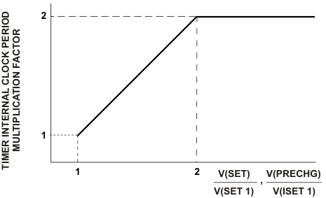 Figure 26. Safety Timer Internal Clock Slowdown
The effective charge safety timer value can then be expressed as follows:
Effective precharge timeout = t(PRECHG) + t(PCHGADD)
Effective charge safety timeout = t(CHG) + t(CHGADD)
The added timeout values, t(PCHGADD), t(CHGADD), are equal to the sum of all time periods when either the thermal loop or DPPM loops were active. The maximum added timeout value is internally limited to 2 × t(CHG) or 2 × t(PRECHG)
8.3.2.4 Functionality Guide — System Power and Charge Management
Table 8. Charge Management
| FAST CHARGE(1) | PRECHARGE CURRENT | TERMINATION | CHARGE VOLTAGE | PRECHARGE VOLTAGE | SAFETYTIMER TIMEOUT | POWER UP DEFAULT | ||
|---|---|---|---|---|---|---|---|---|
| CHARGE CURRENT VALUE | CHARGE CURRENT SCALING | CURRENT | CURRENT SCALING | |||||
| IO(BAT), Programmable, 1.5 A (maximum) | 25%, 50%, 75%, 100% of IO(BAT) | 10% of IO(BAT) |
I(TERM), 10% of IO(BAT) | 25%, 50%, 75%, 100% of I(TERM) value | 4.2 V or 4.36 V |
3 V | Programmable | Charger OFF |
| Set through external resistor | Set through I2C | Fixed ratio | Fixed ratio | Set through I2C | Set through I2C | Fixed | Set through external resistor | |
Table 9. Power Path Management
| INPUT CURRENT LIMIT | INPUT CONNECTED TO OUT PIN | POWER UP DEFAULT | |||
|---|---|---|---|---|---|
| AC PIN | USB PIN | INPUT POWER TO SYSTEM | BATTERY TO SYSTEM | ||
| 2.5 A typical | 100 mA maximum or 500 mA maximum or 2.5 A typical |
#1 – #2 – #3 – |
AC USB Battery (when AC pin power and USB pin power are not detected ) |
Battery connected to system, independently of battery voltage | Input Power to System, USB mode selected, 100 mA max |
| Internal fixed current limit | Set through I2C | Automatic internal algorithm | Set through I2C, overrides internal algorithm | ||
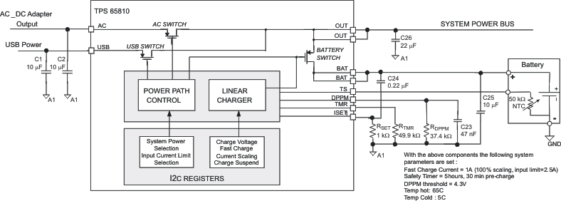 Figure 27. Required External Components, Recommended Values, External Connections
8.3.3 Linear Regulators
The TPS65810 offers nine integrated linear regulators, designed to be stable over the operating load range with use of external ceramic capacitors, as long as the recommended filter capacitor values (see Figure 51 and the Pin Configuration and Functions section) are used. The output voltage can be programmed through I2C (LDO0-2, LDO3-5) or have a fixed output voltage.
8.3.3.1 Simplified Block Diagram
Figure 28 shows a simplified block diagram for the LDOs.
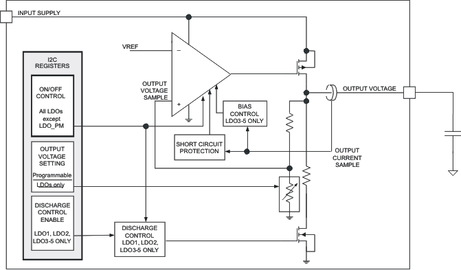 Figure 28. Simplified Block Diagram
8.3.3.2 Connecting the LDO Input Supply
Both LDO1-2 and LDO3-5 have uncommitted input power supply pins (VIN_LDO12, VIN_LDO35), which must be externally connected to the OUT pin. Optionally the LDO0-2 and LDO3-5 input supplies can be connected to the output of the available buck converters SM1 or SM2, as long as the resulting overall power-up sequence meets the system requirements.
The RTC_OUT, SIM, LDO0 and LDO_PM linear regulators are internally connected to the OUT pin.
8.3.3.3 ON/OFF Control
All the LDOs, with exception of LDO_PM LDO, have a ON and OFF control which can be set through I2C commands, facilitating host management of the distinct system power rails. The LDO_PM LDO ON and OFF control is internally hard-wired, and it is set to ON when either the AC or USB input power is detected.
8.3.3.4 Output Discharge Switch
LDO1, LDO2 AND LDO3-5 have integrated switches that discharge each output to ground when the LDO is set to OFF by an I2C command. The output discharge switch function can be disabled by using I2C register control bits. The discharge switches are enabled after the initial power-up
8.3.3.5 Special Functions
The RTC_OUT, SIM (Subscriber line interface module) and LDO_PM linear regulators are designed to support lower load currents. The SIM and RTC_LDO have low leakage in OFF mode, with the input pin voltage above or below the output pin voltage. The LDO_PM can be used for USB enumeration, or a status indication of input power connection.
8.3.3.6 Output Voltage Monitoring
Internal power-good comparators monitor the LDO outputs and detect when the output voltage is below 90% of the programmed value. This information is used by the TPS65810 to generate interrupts or to trigger distinct operating modes, depending on specific I2C register settings. See the Interrupt Controller and System Sequencing section for additional details.
8.3.3.7 Functionality Guide — Linear Regulators
Table 10. Selectable Output Voltage LDO
| SUPPLY | ON/OFF CONTROL | OUTPUT DISCHARGE SWITCH | OUTPUT VOLTAGE (V), SET THROUGH I2C | IO MAX (mA) |
ACCURACY % | POWER UP DEFAULT | ||
|---|---|---|---|---|---|---|---|---|
| NUMBER OF STEPS | AVAILABLE VALUES (V) | |||||||
| LDO1 | Yes, set through I2C | Yes, enabled through I2C | 8 | 1.25/1.5/1.8/2.5/2.85/3/3.2/3.3 | 150 | 3 | OFF, 1.25 V | |
| LDO2 | Yes, set through I2C | Yes, enabled through I2C | 8 | 1.25/1.5/1.8/2.5/2.85/3/3.2/3.3 | 150 | 3 | OFF, 3.3 V | |
| SIM | Yes, set through I2C | no | 2 | 1.8 / 2.5 | 8 | 2 | ON, 2.5 V | |
Table 11. Programmable Output Voltage LDO
| SUPPLY | ON/OFF CONTROL | OUTPUT DISCHARGE SWITCH | OUTPUT VOLTAGE (V), SET THROUGH I2C | IO MAX (mA) | ACCURACY % | POWER UP DEFAULT | ||
|---|---|---|---|---|---|---|---|---|
| RANGE | NUMBER OF STEPS | MINIMUM STEP | ||||||
| LDO3 | Yes, set through I2C | Yes, enabled through I2C | 1.224 to 4.46 | 128 | 25 mV | 100 | 3 | OFF, 1.505 V |
| LDO4 | Yes, set through I2C | Yes, enabled through I2C | 1.224 to 4.46 | 128 | 25 mV | 100 | 3 | OFF, 1.811 V |
| LDO5 | Yes, set through I2C | Yes, enabled through I2C | 1.224 to 4.46 | 128 | 25 mV | 100 | 3 | ON, 3.111 V |
Table 12. Fixed-Output Voltage LDOs
| SUPPLY | ON/OFF CONTROL | OUTPUT VOLTAGE (V) | IO MAX (mA) | ACCURACY % | POWER UP DEFAULT | |||
|---|---|---|---|---|---|---|---|---|
| RTC_OUT | Yes, through I2C | 1.5, fixed | 8 | 5 | ON | |||
| LDC0 | 3.3, fixed | 150 | 3 | OFF | ||||
| LDO_PM | NO, enabled internally | 3.3, fixed | 20 | 5 | ON if AC or USB power detected | |||
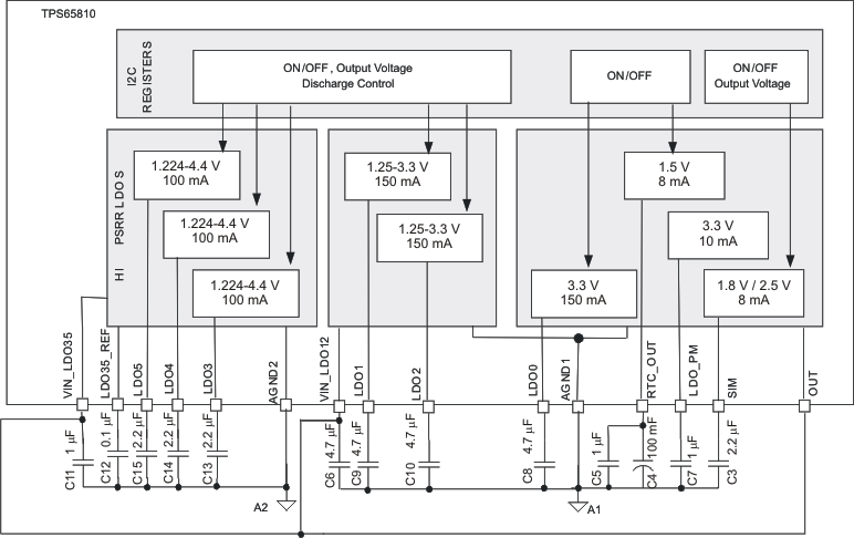 Figure 29. Required External Components, Recommended Values, External Connections
8.3.4 Step-Down Switched-Mode Converters: SM1 and SM2
The TPS65810 device has two high-efficiency, step-down, synchronous converters. The integration of the power stage switching MOSFETs reduces the external component count, and only the external output inductor and filter capacitor are required. The integrated power stage supports 100% duty cycle operation. Multiple operation modes are available, enabling optimization of the overall system performance under distinct load conditions.
The converters have two modes of operation: a 1.5-MHz fixed frequency pulse width modulation (PWM) mode at moderate to heavy loads, and a pulse frequency modulation (PFM) mode at light loads. The converter output voltage is programmable through I2C registers SM1_SET1 and SM2_SET1.
When the SM1/SM2 converters are disabled an integrated switch automatically discharges the converter output capacitor. The discharge switch function can be disabled by setting the control bits DISCHSM1 and DISCHSM2 to LO, in I2C registers SM1_SET2 and SM2_SET2.
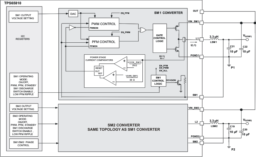 Figure 30. SM1 and SM2 Converter
The TPS65810 SM1 and SM2 buck converters can be set to operate only in PWM mode or to switch automatically between PFM and PWM modes. The average load current is monitored, and the PFM mode is set if the average load current is below the threshold IPFM(ENTER). When in PFM mode the load current is also monitored, and the PWM mode is set when the load current exceeds the threshold IPFM(LEAVE). Use Equation 10 to calculate the thresholds for automatic PFM/PWM switching for the SM1 converter. The same thresholds apply to the SM2 converter by replacing VIN_SM1 by VIN_SM2.

The automatic switching mode is enabled through the control bits PFM_SM1 and PFM_SM2 on I2C registers SM1_SET1 and SM2_SET1.
8.3.4.1 Output Voltage Slew Rate
I2C registers enable setting the output voltage slew rate, when transitioning from one programmed voltage to a new programmed voltage value. These events can be triggered by a new output voltage selection or by switching from a low-power mode (stand-by) to a normal operating mode. During a transition, the output voltage is stepped from the currently programmed voltage to the new target voltage. The slew rate from the initial voltage to the final voltage can be selected using I2C registers, SM1_SET2 and SM2_SET2, ranging from 0.24 mV/μs to 15.36 mV/μs for the SM1 converter and 0.48 to 30.72 mV/μs for the SM2 converter. If the slew rate is set to OFF the output voltage goes from the current value to the programmed value in a single step.
During the transition to stand-by mode the power-good comparators are disabled.
8.3.4.2 Soft-Start
SM1 and SM2 have an internal soft-start circuit that limits the inrush current during start-up. An initial delay (170 μs typical) from the converter enabled command to the converter effectively being operational is required, to assure that the internal circuits of the converter are properly biased. At the end of that initial delay the soft-start is initiated, and the internal compensation capacitor is charged with a low value current source. The soft-start time is typically 750 μs, with the output voltage ramping from 5% to 95% of the final target value.
8.3.4.3 Dropout Operation at 100% Duty Cycle
The TPS65810 buck converters offer a low input to output voltage difference while still maintaining operation when the duty cycle is set to 100%. In this mode of operation the P-channel switch is constantly turned on, enabling operation with a low input voltage. The dropout operation begins if Equation 11 is true:

where
- I(L1) = Output current plus inductor ripple current
- RL = DC resistance of the inductor
Equation 11 can be also used for the SM2 converter, replacing SM1 by SM2 and L1 by L2.
8.3.4.4 Output Voltage Monitoring
The output voltage of converters SM1 and SM2 is monitored by internal comparators, and an output low voltage condition is detected when the output voltage is below 90% of the programmed value. The power-good status for SM1 and SM2 is accessible through I2C, see interrupt controller section for more details.
The power-good comparators for SM1 and SM2 are disabled during the transition to stand-by mode operation. They are enabled when the transition to stand-by mode is complete.
8.3.4.5 Stand-by Mode
Using the I2C SM1 and SM2 can be set in stand-by mode. In stand-by mode the PFM operation mode is set and the output voltage is defined by I2C registers SM1_STANDBY and SM2_STANDBY, and it can be set to a value different than the normal mode output regulation voltage. The stand-by mode can also be set by the GPIO pins, if those are configured as control pins that define the SM1 and SM2 operating modes.
8.3.4.6 PWM Operation
During PWM operation the converters use a fast response voltage mode controller scheme with input voltage feed-forward, enabling the use of small ceramic input and output capacitors. At the beginning of each clock cycle the P-channel MOSFET switch is turned on, and the oscillator starts the voltage ramp. The inductor current ramps up until the ramp voltage reaches the error amplifier output voltage, when the comparator trips and the P-channel MOSFET switch is turned off. Internal adaptative break-before-make circuits turn on the integrated N-channel MOSFET switch after an internal, fixed dead-time delay, and the inductor current ramps down, until the next cycle is started. When the next cycle starts the ramp voltage is reset to its low value and the P-channel MOSFET switch is turned on again.
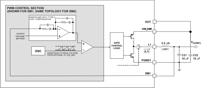 Figure 31. PWM Operation
The integrated power MOSFETs current is monitored at all times and the power MOSFET is turned off if the internal short circuit current limit is reached.
8.3.4.7 Phase Control in PWM Mode
The SM1 and SM2 converters operate synchronized to each other when both are in PWM mode, with converter SM1 as the master. I2C control register bits S1S2PHASE in register SM1_SET2 enables delaying the SM2 PWM clock with respect to SM1 PWM clock, selecting a phase shift from 0 to 270 degrees. The out-of-phase operation reduces the average current at the input node, enabling use of smaller input filter capacitors when both converters are connected to the same input supply.
8.3.4.8 PFM Mode Operation
Using the I2C interface the SM1 and SM2 converters can have the automatic power saving PFM mode enabled. When the PFM mode is set the switching frequency is reduced and the internal bias currents are decreased, optimizing the converter efficiency under light load conditions.
In PFM mode, the output voltage is monitored by a voltage comparator, which regulates the output voltage to the programmed value, VO(SM1). If the output voltage is below VO(SM1), the PFM control circuit turns on the power stage, applying a burst of pulses to increase the output voltage. When the output voltage exceeds the target regulation voltage, VO(SM1), the power stage is disabled, and the output voltage drops until it is below the regulation voltage target, when the power stage is enabled again.
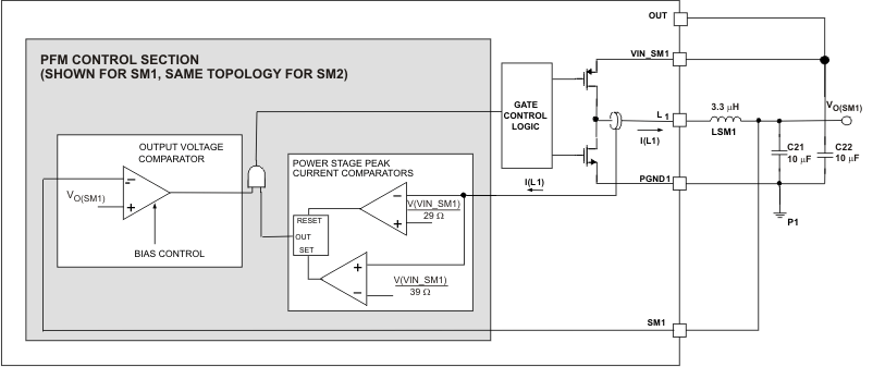 Figure 32. PFM Mode Operation
During burst operation two current comparators control the power stage integrated MOSFETs. These comparators monitor the instantaneous inductor current and compare it to the internal thresholds IPFM(ENTER) and IPFM(LEAVE), turning the P-channel switch on if the inductor current is less than IPFM(LEAVE) and turning it off if the inductor current exceeds IPFM(ENTER). The N-channel switch is turned on when the P-channel MOSFET is off.
The PFM output voltage comparator quiescent current may be reduced using the I2C register bits PFM_RPL1 and PFM_RPL2 in registers SM1_SET and SM2_SET. The voltage comparator quiescent current is reduced if PFM_RPL1 and PFM_RPL2 bits are set to LO, and the comparator response time (tCOMP, see Figure 33) increases. A reduction in quiescent current increases the converter efficiency at light loads, at the expense of a larger output voltage ripple when in PFM mode.
The ripple is minimized if PFM_RPL1 and PFM_RPL2 bits are set to HI, at the expense of reduced efficiency under light loads. The operation under low and high ripple settings is described in Figure 33.
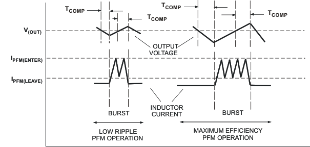 Figure 33. PFM Mode Operation Waveforms
When a burst of pulses is generated, the PFM current comparators control the power-stage MOSFETs to limit the inductor current to a value between the thresholds IPFM(LEAVE) and IPFM(ENTER). The number of pulses in a burst cycle is proportional to the load current, and the average current is always below IPFM(LEAVE) once PFM operation is set. The typical burst operation in PFM mode is shown in Figure 34.
 Figure 34. Typical Burst Operation in PFM Mode
The PFM operation is disabled and PWM operation set if one of the following events occur during PFM operation:
- The total burst operation time exceeds 10 μs (typical).
- The output voltage falls below 2% of the target regulation voltage.
The PFM mode can be disabled through the serial interface to force the individual converters to stay in fixed frequency PWM mode.
8.3.4.9 Functionality Guide — Switched-Mode Step-Down Converters
Table 13. Buck Converters, I2C Programmable Output Voltage
| SUPPLY | PFM MODE | STANDBY MODE | OUTPUT VOLTAGE (V), SET THROUGH I2C, SEPARATE SETTINGS FOR NORMAL OR STANDBY MODE | IO MAX (mA) | PWM FREQUENCY AND PHASE | SLEW RATE, mV/μs, SET THROUGH I2C | POWER UP DEFAULT | |||||
|---|---|---|---|---|---|---|---|---|---|---|---|---|
| RANGE | NUMBER OF STEPS | MIN STEP | ACC. (%) | RANGE | NO. OF STEPS | MIN STEP | ||||||
| SM1 | PFM/PWM with automatic mode selection or PWM only. | Standby mode with distinct voltage available. Standby mode set through I2C or with GPIO pin | 0.6 to 1.8 | 32 | 40 mV | 3 | 600 | 1.5 MHz, 0° | 0, 0.24 to 15.36 | 8 | 0.24 | OFF, skip mode off, PWM only, 1.24 V (on/sby), 15.36 mV/μs |
| SM2 | Mode of operation set through I2C | 1 to 3.4 | 32 | 80 mV | 3 | 600 | 1.5 MHz, 0/90/180 270°, with respect to SM1, set through I2C | 0, 0.48 to 30.72 | 8 | 0.48 | OFF, skip mode on, PWM/PFM, 3.32 V (on/sby), 180°, 30.72 mV/μs | |
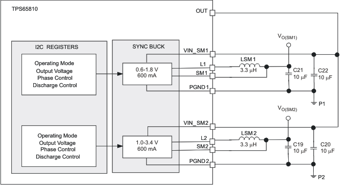 Figure 35. Required External Components, Recommended Values, External Connections
8.3.5 Analog-to-Digital Converter
8.3.5.1 Overview
The TPS65810 has a 10-bit integrated successive approximation A/D, capable of running A/D conversions on eight distinct channels in a variety of modes. Two of the eight channels are connected to uncommitted pins ANLG1 and ANLG2, and can be used to convert external voltages. The other six channels monitor system parameters which are critical to the overall system monitoring. The channel selection is set through I2C.
A dedicated set of I2C registers enables configuration of the ADC to perform a conversion cycle with either a single conversion or a multiple conversions. The ALU generates a data set containing maximum value detection, minimum value detection and average value calculation for each conversion cycle. Each cycle can be performed a single time or multiple times.
8.3.5.2 Input Channels
The channels listed in Table 14 are available for selection through the I2C register ADC_SET bits CHSEL_SET bits.
Table 14. ADC Input Channel Overview
| CHANNEL | CONNECTION | PARAMETER SAMPLED | VOLTAGE RANGE UNDER NORMAL OPERATING CONDITIONS | SPECIAL FEATURES | FULL SCALE READING (INTERNAL REFERENCE SELECTED) | LSB VALUE |
|---|---|---|---|---|---|---|
| CH1 | ANLG1 pin | User defined | User defined | Internal pullup current source programmable through I2C: 0/ 10/50/60 μA |
2.535 V | Full scale reading ÷ 1023 |
| CH2 | ANLG2 pin | 2.535 V | ||||
| CH3 | ISET1 pin | Voltage proportional to charge current | 0 V (charger off) to 2.525 V (fast charge) | — | 2.535 V | |
| CH4 | TS pin | Voltage proportional to pack temperature | 0 V (short) to 4.7V (no thermistor) | No internal pullup current, use external pullup resistor to bias pack thermistor | 2.535 V | |
| CH5 | Internal junction temperature | Voltage proportional to IC junction temperature | 1.85 V at TJ = 25°C, –6.5 mV/°C slope typ | — | 2.535 V | |
| CH6 | RTC_OUT pin | Internal LDO output voltage | 0 V to 3.3 V | — | 4.7 V | |
| CH7 | OUT pin | System power bus voltage | 0 V to 4.4 V | — | 4.7 V | |
| CH8 | BAT pin | Battery pack positive terminal voltage | 0 V to 4.4 V | — | 4.7 V |
8.3.5.3 Functional Overview
The TPS65810 ADC can be subdivided in four sections which are defined as follows:
-
Input Selection The input selection section has two major blocks, the input bias control and an 8 channel MUX. The input bias control provides the bias currents that are applied to pins ANLG1 and ANLG2. The bias currents for pins ANLG1 and ANLG2 are set on I2C register ADC_WAIT.
The ANLG1 pin current source is automatically enabled when the input power is detected, providing the required setup to measure a battery ID resistor (ANLG1 pin). ANLG1 and ANLG2 can be used to measure external resistive loads or analog voltages. The bias current sources are always connected to the OUT pin internally.
The internal MUX connects one of the monitored analog inputs to the ADC engine, following the selection defined on register ADC_SET.
-
ADC Engine The ADC engine uses an internal or external voltage reference, as defined by the ADC_REF bit on the ADC_SET control register. If the internal reference is selected ADC_REF is connected to an internal LDO that regulates the ADC_REF pin voltage to generate the ADC supply and internal voltage reference. The internal LDO maximum output current is 6 mA typical, and a conversion must be started only after the external capacitor is fully charged.
If an external reference is used it must be connected to the ADC_REF pin. When an external reference is selected the internal LDO connected to ADC_REF is disabled. Care must be taken when selecting an external reference as the ADC reference voltage, as it affects the ADC LSB absolute value.
-
Trigger Control and Synchronization The ADC engine starts a conversion of the selected input when the trigger control circuit sends a start command. The trigger control circuit starts the ADC conversion and transfers the ADC output data to the arithmetic logic unit (ALU) at the end of the conversion. It also synchronizes the data transfer from the ALU to the I2C ADC_READING register at the end of a conversion cycle, and generates the ADC status information sent to the ADC registers.
An ADC engine conversion is triggered by the TPS65810 trigger control circuit using either an internal trigger or an external trigger. The internal trigger is automatically generated by the TPS65810 at the end of each ADC engine conversion, following the timing parameters set on I2C registers ADC_SET, ADC_DELAY and ADC_WAIT.
The GPIO3 pin can be used as an external trigger if the bit ADC_TRG_GPIO3 is set HI, in the I2C register ADC_DELAY. In the external trigger mode a new conversion is started after the GPIO3 pin has an edge transition, following the timing parameters set on I2C registers ADC_SET, ADC_DELAY and ADC_WAIT.
-
Arithmetic Logic Unit (ALU) The ALU performs mathematical operations on the ADC output data as defined by the I2C ADC_READING registers. It executes average calculations or minimum /maximum detection. The result of the calculations is stored in a 11 bit accumulator register (1 bit allocated for carry-over). The accumulator value is transferred to the I2C data register at the end of a conversion cycle.
Figure 36 shows a simplified block diagram for the ADC.
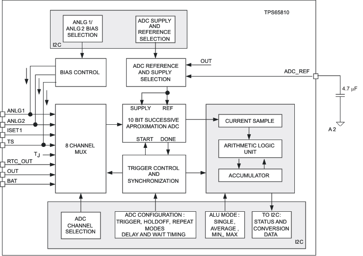 Figure 36. ADC Simplified Block Diagram
8.3.5.3.1 ADC Conversion Cycle
A conversion cycle includes all the steps required to successfully sample the selected input signal and transfer the converted data to the I2C, generating an interrupt request to the host ( pin: HI→LO). The number of individual conversions (samples) in a conversion cycle is defined by the I2C ADC_SET register bits READ_MODE settings, and can range from a single sample to 256 samples. The conversion cycle settings for the ALU is defined by register ADC_READING and it can be set to average, maximum value detection, minimum value detection or no processing (ADC engine output loaded in the accumulator directly).
The conversion cycle begins with the first sampling and ends when the following occurs:
- The required ALU operations are performed on the final sample, and
- The ALU accumulator data is transferred to the I2C ADC_READING register, and
- The register bit ADC_STATUS in the ADC_READING register is set to LO.
A conversion cycle is always started by the external host when the ADC_EN bit in the ADC_SET register is toggled from LO to HI by a I2C write operation. Resetting the ADC_EN bit to LO before the current conversion cycle ends (INT: LO → HI, ADC_STATUS bit set to LO) is not recommended, as the ADC keeps its current configuration until the current conversion cycle ends.
At the end of a conversion cycle the output data is stored at registers in the ALU block. The ADC_STATUS bit is set to LO ( DONE ) and an interrupt is generated (INT pin: HI→LO ) if the ADC_STATUS bit is unmasked, at the interrupt masking registers INT_MASK. It must be noted that the minimum, maximum and average values are ALWAYS calculated by the ALU for each conversion cycle.
The value loaded in the I2C registers ADC READING_HI and ADC READING_LO at the end of a conversion cycle is defined by control bits ADC_READ0 and ADC_READ1 in register ADC READING_HI. The average, minimum, maximum, and last-sample values for a conversion cycle can be read if the external host executes an I2C write operation, changing the values of bits ADC_READ0 and ADC_READ1, followed by an I2C read operation on registers ADC READING_HI and ADC READING_LO. The minimum, maximum, average, and last values have the same value if a conversion cycle with only one sample is executed.
The ADC_READ0 and ADC_READ1 bits can not be modified during the execution of a conversion cycle. A new conversion cycle must be started only after the current conversion cycle is completed, by toggling the ADC_EN bit from HI to LO and HI again.
8.3.5.3.2 External Trigger Operation
The trigger control circuit can be programmed to use an external signal to start a conversion. The TPS65810 GPIO3 input is configurable as an ADC trigger, with ADC conversion starting on either a rising edge or falling edge. When using an external trigger the trigger delay, trigger wait time delay and trigger hold-off mode can be programmed using I2C registers.
The procedure to start an externally-triggered conversion cycle has the following steps:
- Verify that the current conversion cycle has ended (ADC_STATUS = LO, I2C register ADC_READING_HI)
- Set ADC_EN = LO
- Configure ADC sampling mode, ALU mode, trigger parameters, and so forth
- Set ADC_EN = HI
After step 4 the ADC is armed, waiting for an external trigger detection to start a conversion cycle. Similarly to the non-triggered mode, the ADC configuration must not be modified until the current conversion cycle ends. Note that in the external trigger mode the current cycle does not end if the converter is armed and an external trigger is not detected.
8.3.5.3.3 Detecting an External Trigger Event
An external trigger event is detected when the GPIO3 input has an edge that matches the edge detection programmed in the EDGE bit, at the I2C register ADC_DELAY. The internal ADC trigger can be delayed with respect to the external trigger signal edge. The delay time value is set by the ADC_DELAY register bits DELAY_n, and can range from 0 μs (no delay) to 750 μs. A conversion is started only if the external trigger remains at its active level when the delay time expires, as shown in Figure 37. In a positive-edge detection the active trigger level is HI; in a negative-edge detection the active trigger level is LO.
 Figure 37. ADC Conversion Triggered by GPIO3 Positive Edge Triggered Active Level Hi
8.3.5.3.4 Executing Multiple-Sample Cycles With an External Trigger
When executing conversion cycles that require multiple samples it may be desirable to synchronize the input signal conversion using either an external trigger that has a periodic repetition rate or an external asynchronous trigger that indicates when the external input signal being converted is valid. The TPS65810 has additional operating modes and timing parameters that can be programmed using the I2C to configure multiple sample conversion cycles.
In multiple sample cycles the host can select the wait time between samples using the bits WAITn in the ADC_WAIT register to set the wait time between samples. The wait time is measured between the end of a conversion and the start of a new conversion.
With the default power-up settings (HOLDOFF=LO, ADC_DELAY register), the TPS65810 executes a multiple-sample conversion cycle if the first sample is taken when the trigger is at its active level. Subsequent samples are converted at the end of the wait time, even if the trigger returns to the non-active level. The external trigger level edge is ignored until the current conversion cycle ends.
 Figure 38. ADC Conversion Triggered by GPIO3 Positive Edge Triggered Active Level Hi, Holdoff = LC
If the sample conversion needs to be synchronized with an external trigger, during multiple sample conversion cycles, the control bit HOLDOFF must be set to HI. When the holdoff mode is active, the internal trigger starts a sample conversion only if the external trigger was detected and is at its active level at the end of the wait time, as shown in Figure 39.
 Figure 39. ADC Conversion Triggered by GPIO3 Positive Edge Triggered Active Level HI,
Holdoff = HI, Four Sample Cycles
When the multiple sample cycles are executed the host must configure the maximum and minimum limits for the ADC output using registers DLOLIM1, DLOLIM2, DHILIM1 and DHILIM2. A conversion cycle ends if any individual conversion result exceeds the maximum limit value or is below the minimum limit value. When an out of limit conversion is detected an interrupt is sent to the host, and the ADC_STATUS bit on register ADC READING_HI is set to DONE.
8.3.5.3.5 Continuous Conversion Operation (Repeat Mode)
The TPS65810 ADC can be set to operate in a continuous conversion mode, with back-to-back conversion cycles executed. The REPEAT mode is targeted at applications where an input is continuously monitored for a period of time, and the host must be informed if the monitored input is out of the range set by I2C registers DLOLIM1, DLOLIM2, DHILIM1 and DHILIM2. In REPEAT mode each conversion is started when the ADC trigger (internal or external) is detected, and a new conversion cycle is started when the current conversion cycle ends. All the trigger and sampling modes available for normal conversion cycles are available in repeat mode. Executing I2C read operations to get the ADC readings for average, minimum, maximum and last sample values is possible in REPEAT mode. However, TI does not recommend this operation, as the REPEAT mode does not generate a DONE status flag making it difficult to synchronize the ADC data reading to the end of a conversion cycle.
TI recommends using these steps for the REPEAT mode:
- Configure the ADC conversion cycle: trigger mode, sample mode, select input signal, or others.
- Configure the HI and LO limits for the ADC readings
- Set the ADC_DELAY register bit REPEAT to HI
- Toggle ADC_DELAY register bit ADC_EN bit from LO to HI
- Monitor the INT pin. An interrupt triggered by ADC_STATUS = LO indicates that the selected input signal is out of range
To exit the continuous mode the host must follow the steps below, if external trigger mode was set:
- Exit external trigger mode
- Set REPEAT bit to LO, effectively terminating the repeat mode. This generates an additional conversion; at the end of this conversion the ADC is ready for a new configuration.
- Set ADC_EN to LO after on-going conversion ends.
To exit the continuous mode the host must follow the steps below, if internal trigger mode was set:
- Set REPEAT bit to LO, effectively terminating the repeat mode.
- Set ADC_EN to LO, after on-going conversion ends
8.3.5.3.6 ADC Input Signal Range Setting
The registers DHILIMn and DLOLIMn can be used by the host to set maximum and minimum limits for the DAC engine output. At the end of each conversion the ADC output is checked for the maximum and minimum limits, and a status flag is set if the converted data exceeds the high limit or is under the low limit. In multiple sample operation the converted data range is checked when all programmed samples have been converted.
The host can mask or unmask interrupts caused by the ADC range status bits using the INT_MASKn registers.
8.3.5.3.7 ADC State Machine
Figure 40 shows the ADC state machine with all the trigger and operation modes.
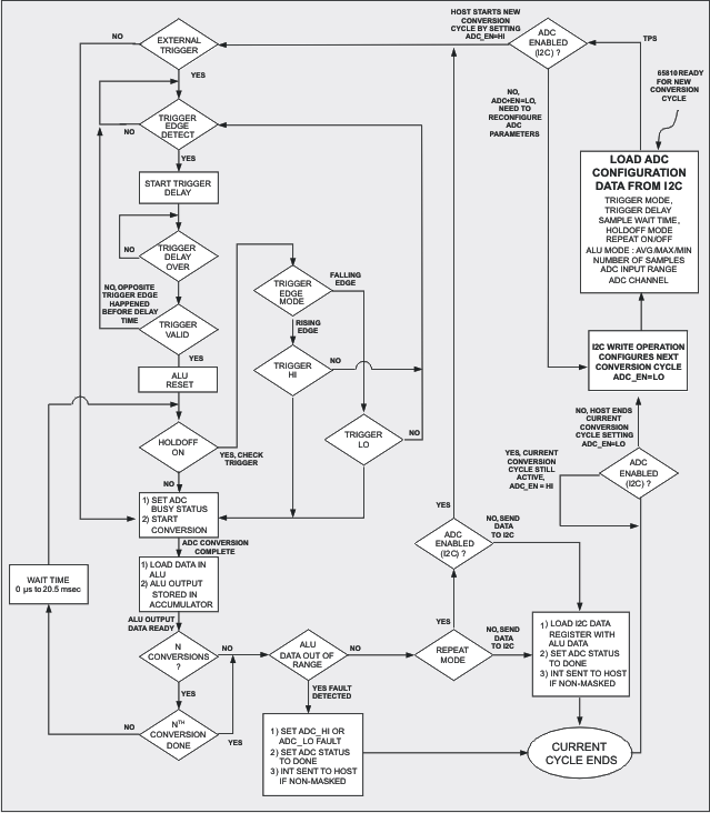 Figure 40. Trigger and Operation Modes for the ADC State Machine
8.3.5.4 Battery Detection Circuit
The ANLG1 pin has an internal current source connected between OUT and ANLG1, which is automatically turned on when the OUT pin voltage exceeds the minimum system voltage set by the SYS_IN pin external resistive divider. The current levels for ANLG1 pin can be programmed through I2C register ADC_WAIT, bits BATID_n. An integrated switch discharges the BAT pin to AGND1 when V(ANLG1)> V(OUT) – V(NOBATID), enabling implementation of a battery removal function if an external pack resistor ID is connected between ANLG1 and ground.
The ANLG1 pin may be used to monitor other parameters than a pack ID resistor. When ANLG1 pin is used as a generic ADC analog input V(ANLG1) must never exceed V(OUT) – V(NOBATID), to avoid undesired battery discharge caused by activation of the battery pin discharge circuit.
8.3.5.5 Functionality Guide – Analog to Digital Converter
Table 15. 10-Bit Successive Approximation ADC
| ADC INPUT CHANNELS | TRIGGER MODE | CONVERSION COUNT | CONVERTER MODE | TRIGGER DELAY | WAIT TIME, MULTIPLE CONVERSIONS | POWER UP DEFAULT | ||
|---|---|---|---|---|---|---|---|---|
| INTERNAL | EXTERNAL | RANGE | MIN STEP | |||||
| Charge Current, Thermistor temperature, IC junction temperature, RTC_OUT voltage, OUT voltage, Battery voltage | ANLG1 and ANLG2 voltages | GPIB, I2C driven, Repeat | 1, 4, 8, 16, 32, 64, 128, 256 | Single, Average, Find max value, Find min value | 0 to 750 μs, 16 steps |
50 μs | μs: 20, 40, 60, 80, 160, 240, 320, 640 ms: 1.28, 1.92, 2.56, 5.12, 10.24, 15.36, 20.48 |
ADC off |
| Fixed internally | Selectable through I2C | Selectable through I2C | Selectable through I2C | Selectable through I2C | Selectable through I2C | Selectable through I2C | Selectable through I2C | |
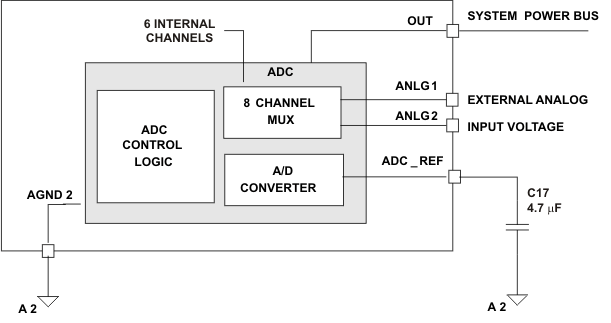 Figure 41. Required External Components, Recommended Values, External Connections
8.3.6 LED and Peripheral Drivers
8.3.6.1 White LED Constant Current Driver
The TPS65810 has an integrated boost converter (SM3) that is optimized to drive white LEDs connected in a series configuration. Up to six series white LEDs can be driven, with programmable current and duty cycle adjustable through a dedicated I2C register.
The SM3 boost converter (SM3) has a 30-V, 500-mA, low-side integrated power stage switch that drives the external inductor. Another integrated 30-V, 25-mA switch (LED switch) is used to modulate the brightness of the external white LEDs. Figure 42 shows a simplified block diagram.
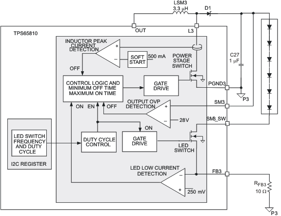 Figure 42. Simplified Block Diagram
The SM3 converter operates like a standard boost converter. The LED current is defined by the value of the external resistor RFB3, connected from pin FB3 to AGND1. The integrated power stage switch control monitors the LED switch current (FB3) and the integrated power stage switch current, implementing a topology that effectively regulates the LED current independently of the input voltage and number of LEDs connected. The high voltage rating of the integrated switches enables driving up to six white LEDs, connected in a series configuration.
The internal LED switch, in series with the external LEDs, disconnects the LEDs from ground during shutdown. In addition, the LED switch is driven by a PWM signal that sets the duty cycle, enabling adjustment to the average LED current by modifying the settings of the I2C register SM3_SET. With this control method, the LED brightness depends on the LED-switch duty cycle only, and is independent of the PWM control signal.
The duty cycle control used in the SM3 converter LED switch is implemented by generating a burst of high frequency pulses, with a pattern that is repeated periodically. For a duty cycle of 50%, all of the high frequency pulses have a 50% duty cycle. The duty cycle control sets individual pulses to 100% duty cycle when increasing the LED_PWM output duty cycle; for decreasing LED_PWM output duty cycles, individual pulses are set to 0% duty cycle. An example of distinct duty cycles is shown in Figure 43, the sum of the individual pulses ON and OFF-time over the repetition period are equivalent to the duty cycle obtained with traditional single-pulse duty cycle circuits.
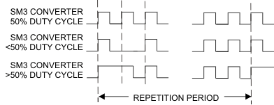 Figure 43. Example of Distinct Duty Cycles
The repetition period can be set using the register SOFT_RESET control bit SM3_LF_OSC to either 183 Hz (HI) or 122 Hz (LO). Each repetition period has a total of 256 pulses, enabling a resolution of 0.4% when programming the duty cycle.
8.3.6.1.1 SM3 Control Logic Overview
The SM3 boost converter operates in a pulse frequency modulation (PFM) scheme with constant peak current control. This control scheme maintains high efficiency over the entire load current range and enables the use of small external components, as the switching frequency can reach up to 1 MHz depending on the load conditions. The LED current ripple is defined by the external inductor size.
The converter monitors the sense voltage at pin FB3, and turns on the integrated power stage switch when V(FB3) is below the 250-mV (typical) internal reference voltage and the LED Switch is ON, starting a new cycle. The integrated power switch turns off when the inductor current reaches the internal 500-mA (typical) peak current limit, or if the switch is on for a period longer than the maximum on-time of 6 μs (typical). The integrated power switch also turns off when the LED switch is set to OFF. As the integrated power switch is turned off, the external Schottky diode is forward biased, delivering the stored inductor energy to the output. The main switch remains off until the FB3 pin voltage is below the internal 250-mV reference voltage and the LED switch is turned ON, when it is turned on again.
This PFM peak current control scheme sets the converter in discontinuous conduction mode (DCM), and the switching frequency depends on the inductor, input/output voltage and LED current. Lower LED currents reduce the switching frequency, with high efficiency over the entire LED current range. This regulation scheme is inherently stable, allowing a wide range for the selection of the inductor and output capacitor.
8.3.6.1.2 Peak Current Control (Boost Converter)
The SM3 integrated power stage switch is turned on until the inductor current reaches the DC current limit IMAX(L3) (500 mA, typical). Because of internal delays, typically around 100 ns, the actual current exceeds the DC current limit threshold by a small amount. Use Equation 12 to calculate the typical peak current limit.

The current overshoot is directly proportional to the input voltage, and inversely proportional to the inductor value.
8.3.6.1.3 Soft-Start
All inductive step-up converters exhibit high in-rush current during start-up. If no special precautions are taken, voltage drops can be observed at the input supply rail during start-up, with unpredictable results in the overall system operation.
The SM3 boost converter limits the inrush current during start-up by increasing the current limit in the following three steps:
- 125 mA (typical),
- 250 mA (typical) and
- 500 mA (typical)
The two initial steps (125 mA and 250 mA) are active for 256 power stage switching cycles.
8.3.6.1.4 Enabling the SM3 Converter
The SM3_SET I2C register controls the SM3 LED-switch duty cycle. If the register is set to all zeros SM3 is set to OFF mode. When the host writes a value other than 00 in SM3_SET the SM3 converter is enabled, entering the soft-start phase and then normal operation. The SM3 converter can operate with duty cycles varying from 0.4% to 99.6%, with LED switch frequencies of 122 Hz or 180 Hz. The LED switch operating frequency is set by bit SM3_LF, in the SOFT_RESET register.
8.3.6.1.5 Overvoltage Protection
The output voltage of the boost converter is sensed at pin SM3, and the integrated power stage switch is turned OFF when V(SM3) exceeds the internal overvoltage threshold VOVP3. The converter returns to normal operation when V(SM3) < VOVP3 – VHYS(OVP3).
8.3.6.1.6 Under Voltage Lockout Operation
When the TPS65810 device enters the UVLO mode, the SM3 converter is set to OFF mode with the power stage MOSFET switch and the LED switch open (off).
8.3.6.1.7 Thermal Shutdown Operation
When the TPS65810 device enters the thermal shutdown mode, the SM3 converter is set to OFF mode with the power stage MOSFET switch and the LED switch open (off).
8.3.6.2 PWM Drivers
8.3.6.2.1 PWM Pin Driver
The TPS65810 device offers one low-frequency, open-drain PWM driver, capable of driving up to 150 mA. The PWM frequency and duty cycle are defined by the PWM I2C register settings. The PWM parameters are set in I2C register PWM. Available frequency values range from 500 Hz to 15 kHz, with 8 frequency values and 16 duty cycle options (6.25% each).
8.3.6.2.2 LED_PWM Pin Driver
The TPS65810 has another PWM driver output (pin LED_PWM), which is optimized to drive a backlight LED. The LED_PWM driver controls the external LED current intensity using a pulse-width control method, with duty cycle being set by the I2C register LED_PWM.
The pulse width method implemented generates a burst of high frequency pulses, with a pattern that is repeated periodically. For a duty cycle of 50%, all of the high -frequency pulses have a 50% duty cycle. The duty cycle control sets individual pulses to 100% duty cycle when increasing the LED_PWM output duty cycle; for decreasing LED_PWM output duty cycles individual pulses are set to 0% duty cycle. An example of distinct duty cycles is shown in Figure 44; the sum of the individual pulses on/off time over the repetition period is equivalent to the duty cycle obtained with traditional single-pulse duty cycle circuits.
 Figure 44. Example of Distinct Duty Cycles
The repetition period can be set using the register SOFT_RESET control bit SM3_LF_OSC to either 180 Hz (HI) or 122 Hz (LO). Each repetition period has a total of 256 pulses, enabling a resoltuion of 0.4% when programming the duty cycle. The LED_SET register enables control of the duty cycle through I2C, with duty cycle ranging from 0.4% to 99.6%. Setting the LED_SET register to all zeros forces the LED_PWM pin to 0% duty cycle (OFF).
8.3.6.2.3 RGB Driver
The TPS65810 has a dedicated driver for an RGB external LED. Three outputs are available (pins RED, GREEN, BLUE), with common settings for operation mode (flash on/off, flash period, flash on time), LED current and phase delay between outputs. The TPS65810 RGB driver continually flashes the external LEDs connected to the RED, GREEN and BLUE pins using the flash operation parameters defined in register RGB_FLASH.
The currents for the external LEDs can be programmed through I2C, and external resistors are not required to limit the LED current. However, they can be added to set the LED current if the available I2C values are not compatible with the current application, as shown in Figure 45.
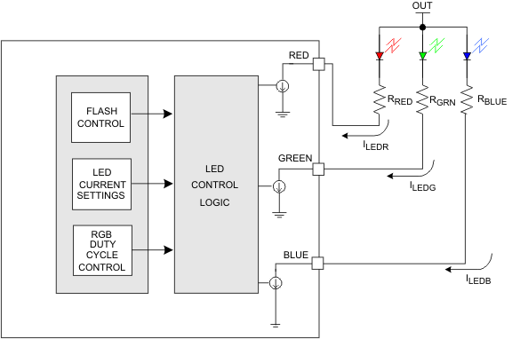 Figure 45. Limiting the External LED Current
The flashing-mode parameters defined in register RGB_FLASH enable setting the flashing period from 1 to 8 seconds in 0.5-sec steps, or to continuous operation. Flashing operation is enabled by setting the FLASH_EN bit in register RGB_FLASH to HI. This bit must be set HI to enable the RGB current-sink channels.
Each driver has an individual duty cycle control. The duty cycle modulation method used is similar to the PWM_LED duty cycle control, with high frequency pulses being generated when the driver (RED, GREEN, or BLUE pins) is ON. The repetition period for the RGB drivers has a total of 32 pulses, enabling a 3.125% resolution when programming the individual RED, GREEN and BLUE drivers duty cycles. The duty cycles for each driver can be set individually using control bits on registers RGB_RED, RGB_GREEN and RGB_BLUE.
The RGB drivers can be programmed to sink 4, 8, or 12 mA, with no external current limiting resistor.
8.3.6.3 Functionality Guide — LED And Peripheral Drivers
Table 16. White Led Constant Current Driver
| DRIVER | PWM | OUTPUT VOLTAGE |
LED CURRENT | EFFICIENCY (%) | POWER UP DEFAULT |
|||
|---|---|---|---|---|---|---|---|---|
| DUTY CYCLE RANGE |
NUMBER OF STEPS | IO (TYP) | MAX | ACCURACY (%) | ||||
| SM3 | Off (0%), 0.4% to 99.6% Set through I2C |
256 | 5 V to 25 V | Set by external resistor | 25 mA | 25 | 80 | Off (0%) |
Table 17. Open-Drain PWM Drivers
| DRIVER | PWM FREQUENCY (kHz) | PWM DUTY CYCLE | IO(MAX)
mA |
POWER UP DEFAULT | ||
|---|---|---|---|---|---|---|
| RANGE | NUMBER OF STEPS | MIN STEP | ||||
| PWM | 0.5/1/1.5/2/3/ 4.5/7.8/15.6 Set through I2C |
Off (0%), 6.25% to 100 Set through I2C |
8 | 6.25% | 150 | Off(0%) |
| LED_PWM | 15.625 or 23.4 , set through I2C | Off(0%), 0.4% to 99.6% Set through I2C |
256 | 0.4% | 150 | Off (0%) |
Table 18. RGB Open-Drain LED Driver
| DRIVER | FLASH PERIOD (SAME FOR RGB) | FLASH ON TIME (SAME FOR RGB) | BRIGHTNESS (INDIVIDUAL R/G/B CONTROL) |
IO mA | POWER UP DEFAULT | ||||||
|---|---|---|---|---|---|---|---|---|---|---|---|
| RANGE | NUMBER OF STEPS | MIN STEP | RANGE | NUMBER OF STEPS | MIN STEP | DUTY (%) | NUMBER OF STEPS | MIN STEPS | |||
| RED, GREEN, BLUE | No flash, or 1 to 8 s Set through I2C |
16 | 0.5 s | 0.1 to 0.6 s Set through I2C |
8 | 0.1 s | Off (0%), 3.125 to 96.87 Set through I2C |
32 | 3.125% | 0/4/8/12 | Flash Off, 0 mA, 0% brightness duty cycle |
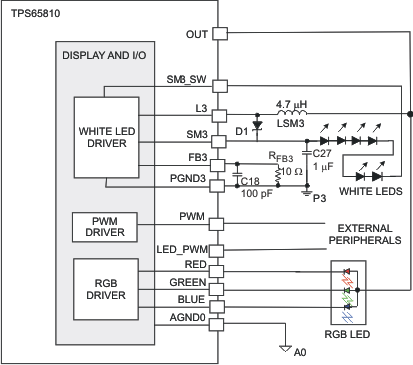 Figure 46. Required External Components, Recommended Values, External Connections
Table 19. SM3 Duty Cycle Settings
| DEC | B7-B0 | DCPU | DEC | B7-B0 | DCPU | DEC | B7-B0 | DCPU | DEC | B7-B0 | DCPU | DEC | B7-B0 | DCPU | ||||
|---|---|---|---|---|---|---|---|---|---|---|---|---|---|---|---|---|---|---|
| 0 | 0000 0000 | – | 52 | 0011 0100 | 0.203 | 104 | 0110 1000 | 0.406 | 156 | 1001 1100 | 0.609 | 208 | 1101 0000 | 0.813 | ||||
| 1 | 0000 0001 | 0.004 | 53 | 0011 0101 | 0.207 | 105 | 0110 1001 | 0.41 | 157 | 1001 1101 | 0.613 | 209 | 1101 0001 | 0.816 | ||||
| 2 | 0000 0010 | 0.008 | 54 | 0011 0110 | 0.211 | 106 | 0110 1010 | 0.414 | 158 | 1001 1110 | 0.617 | 210 | 1101 0010 | 0.82 | ||||
| 3 | 0000 0011 | 0.012 | 55 | 0011 0111 | 0.215 | 107 | 0110 1011 | 0.418 | 159 | 1001 1111 | 0.621 | 211 | 1101 0011 | 0.824 | ||||
| 4 | 0000 0100 | 0.016 | 56 | 0011 1000 | 0.219 | 108 | 0110 1100 | 0.422 | 160 | 1010 0000 | 0.625 | 212 | 1101 0100 | 0.828 | ||||
| 5 | 0000 0101 | 0.02 | 57 | 0011 1001 | 0.223 | 109 | 0110 1101 | 0.426 | 161 | 1010 0001 | 0.629 | 213 | 1101 0101 | 0.832 | ||||
| 6 | 0000 0110 | 0.023 | 58 | 0011 1010 | 0.227 | 110 | 0110 1110 | 0.43 | 162 | 1010 0010 | 0.633 | 214 | 1101 0110 | 0.836 | ||||
| 7 | 0000 0111 | 0.027 | 59 | 0011 1011 | 0.23 | 111 | 0110 1111 | 0.434 | 163 | 1010 0011 | 0.637 | 215 | 1101 0111 | 0.84 | ||||
| 8 | 0000 1000 | 0.031 | 60 | 0011 1100 | 0.234 | 112 | 0111 0000 | 0.438 | 164 | 1010 0100 | 0.641 | 216 | 1101 1000 | 0.844 | ||||
| 9 | 0000 1001 | 0.035 | 61 | 0011 1101 | 0.238 | 113 | 0111 0001 | 0.441 | 165 | 1010 0101 | 0.645 | 217 | 1101 1001 | 0.848 | ||||
| 10 | 0000 1010 | 0.039 | 62 | 0011 1110 | 0.242 | 114 | 0111 0010 | 0.445 | 166 | 1010 0110 | 0.648 | 218 | 1101 1010 | 0.852 | ||||
| 11 | 0000 1011 | 0.043 | 63 | 0011 1111 | 0.246 | 115 | 0111 0011 | 0.449 | 167 | 1010 0111 | 0.652 | 219 | 1101 1011 | 0.855 | ||||
| 12 | 0000 1100 | 0.047 | 64 | 0100 0000 | 0.25 | 116 | 0111 0100 | 0.453 | 168 | 1010 1000 | 0.656 | 220 | 1101 1100 | 0.859 | ||||
| 13 | 0000 1101 | 0.051 | 65 | 0100 0001 | 0.254 | 117 | 0111 0101 | 0.457 | 169 | 1010 1001 | 0.66 | 221 | 1101 1101 | 0.863 | ||||
| 14 | 0000 1110 | 0.055 | 66 | 0100 0010 | 0.258 | 118 | 0111 0110 | 0.461 | 170 | 1010 1010 | 0.664 | 222 | 1101 1110 | 0.867 | ||||
| 15 | 0000 1111 | 0.059 | 67 | 0100 0011 | 0.262 | 119 | 0111 0111 | 0.465 | 171 | 1010 1011 | 0.668 | 223 | 1101 1111 | 0.871 | ||||
| 16 | 0001 0000 | 0.063 | 68 | 0100 0100 | 0.266 | 120 | 0111 1000 | 0.469 | 172 | 1010 1100 | 0.672 | 224 | 1110 0000 | 0.875 | ||||
| 17 | 0001 0001 | 0.066 | 69 | 0100 0101 | 0.27 | 121 | 0111 1001 | 0.473 | 173 | 1010 1101 | 0.676 | 225 | 1110 0001 | 0.879 | ||||
| 18 | 0001 0010 | 0.07 | 70 | 0100 0110 | 0.273 | 122 | 0111 1010 | 0.477 | 174 | 1010 1110 | 0.68 | 226 | 1110 0010 | 0.883 | ||||
| 19 | 0001 0011 | 0.074 | 71 | 0100 0111 | 0.277 | 123 | 0111 1011 | 0.48 | 175 | 1010 1111 | 0.684 | 227 | 1110 0011 | 0.887 | ||||
| 20 | 0001 0100 | 0.078 | 72 | 0100 1000 | 0.281 | 124 | 0111 1100 | 0.484 | 176 | 1011 0000 | 0.688 | 228 | 1110 0100 | 0.891 | ||||
| 21 | 0001 0101 | 0.082 | 73 | 0100 1001 | 0.285 | 125 | 0111 1101 | 0.488 | 177 | 1011 0001 | 0.691 | 229 | 1110 0101 | 0.895 | ||||
| 22 | 0001 0110 | 0.086 | 74 | 0100 1010 | 0.289 | 126 | 0111 1110 | 0.492 | 178 | 1011 0010 | 0.695 | 230 | 1110 0110 | 0.898 | ||||
| 23 | 0001 0111 | 0.09 | 75 | 0100 1011 | 0.293 | 127 | 0111 1111 | 0.496 | 179 | 1011 0011 | 0.699 | 231 | 1110 0111 | 0.902 | ||||
| 24 | 0001 1000 | 0.094 | 76 | 0100 1100 | 0.297 | 128 | 1000 0000 | 0.5 | 180 | 1011 0100 | 0.703 | 232 | 1110 1000 | 0.906 | ||||
| 25 | 0001 1001 | 0.098 | 77 | 0100 1101 | 0.301 | 129 | 1000 0001 | 0.504 | 181 | 1011 0101 | 0.707 | 233 | 1110 1001 | 0.91 | ||||
| 26 | 0001 1010 | 0.102 | 78 | 0100 1110 | 0.305 | 130 | 1000 0010 | 0.508 | 182 | 1011 0110 | 0.711 | 234 | 1110 1010 | 0.914 | ||||
| 27 | 0001 1011 | 0.105 | 79 | 0100 1111 | 0.309 | 131 | 1000 0011 | 0.512 | 183 | 1011 0111 | 0.715 | 235 | 1110 1011 | 0.918 | ||||
| 28 | 0001 1100 | 0.109 | 80 | 0101 0000 | 0.313 | 132 | 1000 0100 | 0.516 | 184 | 1011 1000 | 0.719 | 236 | 1110 1100 | 0.922 | ||||
| 29 | 0001 1101 | 0.113 | 81 | 0101 0001 | 0.316 | 133 | 1000 0101 | 0.52 | 185 | 1011 1001 | 0.723 | 237 | 1110 1101 | 0.926 | ||||
| 30 | 0001 1110 | 0.117 | 82 | 0101 0010 | 0.32 | 134 | 1000 0110 | 0.523 | 186 | 1011 1010 | 0.727 | 238 | 1110 1110 | 0.93 | ||||
| 31 | 0001 1111 | 0.121 | 83 | 0101 0011 | 0.324 | 135 | 1000 0111 | 0.527 | 187 | 1011 1011 | 0.73 | 239 | 1110 1111 | 0.934 | ||||
| 32 | 0010 0000 | 0.125 | 84 | 0101 0100 | 0.328 | 136 | 1000 1000 | 0.531 | 188 | 1011 1100 | 0.734 | 240 | 1111 0000 | 0.938 | ||||
| 33 | 0010 0001 | 0.129 | 85 | 0101 0101 | 0.332 | 137 | 1000 1001 | 0.535 | 189 | 1011 1101 | 0.738 | 241 | 1111 0001 | 0.941 | ||||
| 34 | 0010 0010 | 0.133 | 86 | 0101 0110 | 0.336 | 138 | 1000 1010 | 0.539 | 190 | 1011 1110 | 0.742 | 242 | 1111 0010 | 0.945 | ||||
| 35 | 0010 0011 | 0.137 | 87 | 0101 0111 | 0.34 | 139 | 1000 1011 | 0.543 | 191 | 1011 1111 | 0.746 | 243 | 1111 0011 | 0.949 | ||||
| 36 | 0010 0100 | 0.141 | 88 | 0101 1000 | 0.344 | 140 | 1000 1100 | 0.547 | 192 | 1100 0000 | 0.75 | 244 | 1111 0100 | 0.953 | ||||
| 37 | 0010 0101 | 0.145 | 89 | 0101 1001 | 0.348 | 141 | 1000 1101 | 0.551 | 193 | 1100 0001 | 0.754 | 245 | 1111 0101 | 0.957 | ||||
| 38 | 0010 0110 | 0.148 | 90 | 0101 1010 | 0.352 | 142 | 1000 1110 | 0.555 | 194 | 1100 0010 | 0.758 | 246 | 1111 0110 | 0.961 | ||||
| 39 | 0010 0111 | 0.152 | 91 | 0101 1011 | 0.355 | 143 | 1000 1111 | 0.559 | 195 | 1100 0011 | 0.762 | 247 | 1111 0111 | 0.965 | ||||
| 40 | 0010 1000 | 0.156 | 92 | 0101 1100 | 0.359 | 144 | 1001 0000 | 0.563 | 196 | 1100 0100 | 0.766 | 248 | 1111 1000 | 0.969 | ||||
| 41 | 0010 1001 | 0.16 | 93 | 0101 1101 | 0.363 | 145 | 1001 0001 | 0.566 | 197 | 1100 0101 | 0.77 | 249 | 1111 1001 | 0.973 | ||||
| 42 | 0010 1010 | 0.164 | 94 | 0101 1110 | 0.367 | 146 | 1001 0010 | 0.57 | 198 | 1100 0110 | 0.773 | 250 | 1111 1010 | 0.977 | ||||
| 43 | 0010 1011 | 0.168 | 95 | 0101 1111 | 0.371 | 147 | 1001 0011 | 0.574 | 199 | 1100 0111 | 0.777 | 251 | 1111 1011 | 0.98 | ||||
| 44 | 0010 1100 | 0.172 | 96 | 0110 0000 | 0.375 | 148 | 1001 0100 | 0.578 | 200 | 1100 1000 | 0.781 | 252 | 1111 1100 | 0.984 | ||||
| 45 | 0010 1101 | 0.176 | 97 | 0110 0001 | 0.379 | 149 | 1001 0101 | 0.582 | 201 | 1100 1001 | 0.785 | 253 | 1111 1101 | 0.988 | ||||
| 46 | 0010 1110 | 0.18 | 98 | 0110 0010 | 0.383 | 150 | 1001 0110 | 0.586 | 202 | 1100 1010 | 0.789 | 254 | 1111 1110 | 0.992 | ||||
| 47 | 0010 1111 | 0.184 | 99 | 0110 0011 | 0.387 | 151 | 1001 0111 | 0.59 | 203 | 1100 1011 | 0.793 | 255 | 1111 1111 | 0.996 | ||||
| 48 | 0011 0000 | 0.188 | 100 | 0110 0100 | 0.391 | 152 | 1001 1000 | 0.594 | 204 | 1100 1100 | 0.797 | |||||||
| 49 | 0011 0001 | 0.191 | 101 | 0110 0101 | 0.395 | 153 | 1001 1001 | 0.598 | 205 | 1100 1101 | 0.801 | |||||||
| 50 | 0011 0010 | 0.195 | 102 | 0110 0110 | 0.398 | 154 | 1001 1010 | 0.602 | 206 | 1100 1110 | 0.805 | |||||||
| 51 | 0011 0011 | 0.199 | 103 | 0110 0111 | 0.402 | 155 | 1001 1011 | 0.605 | 207 | 1100 1111 | 0.809 |
Table 20. RGB Duty Cycle Control Settings
| RGB_D4 | RGB_D3 | RGB_D2 | RGB_D1 | RGB_D0 | DC(%) | FLASH_PER3 | FLASH_PER2 | FLASH_PER1 | FLASH_PER0 | P(s) | |
|---|---|---|---|---|---|---|---|---|---|---|---|
| 0 | 0 | 0 | 0 | 0 | 0.00 | 0 | 0 | 0 | 0 | 1 | |
| 0 | 0 | 0 | 0 | 1 | 3.23 | 0 | 0 | 0 | 1 | 1.5 | |
| 0 | 0 | 0 | 1 | 0 | 6.45 | 0 | 0 | 1 | 0 | 2 | |
| 0 | 0 | 0 | 1 | 1 | 9.68 | 0 | 0 | 1 | 1 | 2.5 | |
| 0 | 0 | 1 | 0 | 0 | 12.90 | 0 | 1 | 0 | 0 | 3 | |
| 0 | 0 | 1 | 0 | 1 | 16.13 | 0 | 1 | 0 | 1 | 3.5 | |
| 0 | 0 | 1 | 1 | 0 | 19.35 | 0 | 1 | 1 | 0 | 4 | |
| 0 | 0 | 1 | 1 | 1 | 22.58 | 0 | 1 | 1 | 1 | 4.5 | |
| 0 | 1 | 0 | 0 | 0 | 25.80 | 1 | 0 | 0 | 0 | 5 | |
| 0 | 1 | 0 | 0 | 1 | 29.03 | 1 | 0 | 0 | 1 | 5.5 | |
| 0 | 1 | 0 | 1 | 0 | 32.25 | 1 | 0 | 1 | 0 | 6 | |
| 0 | 1 | 0 | 1 | 1 | 35.48 | 1 | 0 | 1 | 1 | 6.5 | |
| 0 | 1 | 1 | 0 | 0 | 38.70 | 1 | 1 | 0 | 0 | 7 | |
| 0 | 1 | 1 | 0 | 1 | 41.93 | 1 | 1 | 0 | 1 | 7.5 | |
| 0 | 1 | 1 | 1 | 0 | 45.15 | 1 | 1 | 1 | 0 | 8 | |
| 0 | 1 | 1 | 1 | 1 | 48.38 | 1 | 1 | 1 | 1 | Continuous | |
| 1 | 0 | 0 | 0 | 0 | 51.60 | ||||||
| 1 | 0 | 0 | 0 | 1 | 54.83 | ||||||
| 1 | 0 | 0 | 1 | 0 | 58.05 | FLASH_ON2 | FLASH_ON1 | FLASH_ON0 | ON_TIME (s) | ||
| 1 | 0 | 0 | 1 | 1 | 61.23 | 0 | 0 | 0 | 0.1 | ||
| 1 | 0 | 1 | 0 | 0 | 64.50 | 0 | 0 | 1 | 0.15 | ||
| 1 | 0 | 1 | 0 | 1 | 67.73 | 0 | 1 | 0 | 0.2 | ||
| 1 | 0 | 1 | 1 | 0 | 70.95 | 0 | 1 | 1 | 0.25 | ||
| 1 | 0 | 1 | 1 | 1 | 74.18 | 1 | 0 | 0 | 0.3 | ||
| 1 | 1 | 0 | 0 | 0 | 77.40 | 1 | 0 | 1 | 0.4 | ||
| 1 | 1 | 0 | 0 | 1 | 80.63 | 1 | 1 | 0 | 0.5 | ||
| 1 | 1 | 0 | 1 | 0 | 83.85 | 1 | 1 | 1 | 0.6 | ||
| 1 | 1 | 0 | 1 | 1 | 87.08 | ||||||
| 1 | 1 | 1 | 0 | 0 | 90.30 | ||||||
| 1 | 1 | 1 | 0 | 1 | 93.53 | ||||||
| 1 | 1 | 1 | 1 | 0 | 96.75 | ||||||
| 1 | 1 | 1 | 1 | 1 | 99.98 |
Table 21. PWM Frequency and Duty Cycle Settings
| PWM FREQUENCY TABLE | PWM_D DUTY CYCLE | |||||||
|---|---|---|---|---|---|---|---|---|
| PWM_F2 | PWM_F1 | PWM_F0 | F (Hz) | PWM2_D3 | PWM2_D2 | PWM2_D1 | PWM2_D0 | D_cycle (pu) |
| 0 | 0 | 0 | 15600 | 0 | 0 | 0 | 0 | 0.0625 |
| 0 | 0 | 1 | 7800 | 0 | 0 | 0 | 1 | 0.125 |
| 0 | 1 | 0 | 4500 | 0 | 0 | 1 | 0 | 0.1875 |
| 0 | 1 | 1 | 3000 | 0 | 0 | 1 | 1 | 0.25 |
| 1 | 0 | 0 | 2000 | 0 | 1 | 0 | 0 | 0.3125 |
| 1 | 0 | 1 | 1500 | 0 | 1 | 0 | 1 | 0.375 |
| 1 | 1 | 0 | 1000 | 0 | 1 | 1 | 0 | 0.4375 |
| 1 | 1 | 1 | 500 | 0 | 1 | 1 | 1 | 0.5 |
| 1 | 0 | 0 | 0 | 0.5625 | ||||
| 1 | 0 | 0 | 1 | 0.625 | ||||
| 1 | 0 | 1 | 0 | 0.6875 | ||||
| 1 | 0 | 1 | 1 | 0.75 | ||||
| 1 | 1 | 0 | 0 | 0.8125 | ||||
| 1 | 1 | 0 | 1 | 0.875 | ||||
| 1 | 1 | 1 | 0 | 0.9375 | ||||
| 1 | 1 | 1 | 1 | 1 | ||||
8.3.7 General-Purpose I/Os — GPIO 1, 2, 3
The TPS65810 device integrates 3 general-purpose, open-drain ports (GPIOs) that can be configured as selectable inputs or outputs. When configured as outputs the output level can be set to LO or HI through I2C commands. When the GPIOs are configured as inputs the action to be taken when a transition or HI/LO level is detected at the GPIO pin is selectable through I2C.
When configured as inputs the GPIOs can be set in the following modes which are defined as follows:
-
Interrupt request In this mode of operation, a transition at the GPIO pin generates an interrupt request at the interrupt controller. The GPIO interrupt request can be masked at the INT_MASK register. This operation mode is available for GPIOs 1 and 2.
-
SM1 and SM2 control The GPIOs can be used to turn the converters SM1 and SM2 ON/OFF, as well as setting them in stand-by mode. This control mode is available for GPIO1 (SM1 on/off and SM1/SM2 stand-by) and GPIO2 (SM2 on/off control).
-
ADC trigger GPIO3 can be configured as an external ADC trigger. The GPIO3 trigger configuration bit is located at the ADC register ADC_DELAY.
8.3.7.1 GPIOs Input Level Configuration
When using I2C commands, the GPIO1 and GPIO2 pins can be configured as logic output signals or as level-controlled inputs which enables (or disables) the switch mode converters SM1 and/or SM2. These pins may also be configured as rising- or falling-edge-triggered inputs to externally control the generation of an interrupt signal (INT), if desired.
The GPIO3 pin may be used as an external trigger source to start an A/D conversion cycle or as a logic output.
See Figure 47 for a description of the logic used for GPIO1 and GPIO2 inputs when configured for edge-triggered interrupt generation. The signal from the GPIO pin input is double-latched before being sent to the interrupt controller logic. The inversion of the Q output from the first flip-flop must be HI to allow the output latch to be cleared when a READ command occurs. On the initial edge of the GPIO signal, the Q output of the flip-flop is set (HI). The INT line is asserted (LO) after the initial selected edge from the GPIO pin. On the next falling (or rising) edge of the GPIO pin, the interrupt can again be cleared (which allows the INT pin to go back high). The INT signal is cleared (set back HI) after an I2C READ operation is performed.
Thus, two successive edges of the GPIO signal, followed by an I2C READ command, are required to clear the INT pin output. If no I2C READ commands occur, repeatedly applying edges to the GPIO pin does not toggle the state of the INT pin output.
In addition to an I2C READ command after two GPIO edges, a UVLO event or reconfiguration of the GPIO pins as outputs also deasserts the INT signal.
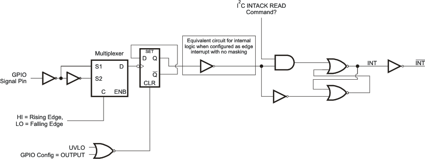 Figure 47. GPIO 1 or GPIO2 Configured as an Interrupt Request Input
8.3.7.2 Function Implementation: I2C Commands Versus GPIO Commands
Some of the GPIO SM1/SM2 control functions overlap I2C register control functions. Table 22 lists the TPS65810 action when the command of the GPIOs and I2C registers commands are not compatible with each other.
Table 22. GPIO Commands and I2C Registers Commands
| SM1 AND SM2 I2C COMMAND | GPIO COMMAND | SM1 OR SM2 MODE SET |
|---|---|---|
| ON/OFF | ||
| CONVERTER DISABLED | CONVERTER DISABLED | DISABLED |
| CONVERTER ENABLED | DON’T CARE | ENABLED |
| DON’T CARE | CONVERTER ENABLED | ENABLED |
| STANDBY | ||
| DO NOT SET STANDBY | DON’T CARE | NORMAL |
| SET STANDBY | SET STANDBY | STANDBY |
| DON’T CARE | DO NOT SET STANDBY | NORMAL |
8.3.7.2.1 GPIO Configuration Table
Table 23 lists the I2C register settings required to program the available GPIO modes. The GPIO pins logic level is available at register SM1_STANDBY, bits B5, B6 and B7.
Table 23. Recommended GPIO Configuration Procedure
| GPIO MODE | I2C REGISTERS | I2C REGISTER BIT SETTING | ADDITIONAL DETAILS |
|---|---|---|---|
| GPIO3 = OUTPUT | GPIO3 | GPIO3I/O=HI AND GPIO3OUT = HI | GPIO3 PIN SET TO HIGH IMPEDANCE MODE |
| GPIO3I/O=HI AND GPIO3OUT = LO | V(GPIO3) = VOL | ||
| GPIO3 =INPUT
ADC CONVERSION START TRIGGER |
GPIO3 AND ADC_DELAY | GPIO3I/O=LO AND ADC_TRG_GPIO3 = HI AND EDGE_GPIO3 = HI | GPIO3 pin rising edge triggers ADC conversion |
| GPIO3I/O=LO AND ADC_TRG_GPIO3 = HI AND EDGE_GPIO3=LO | GPIO3 pin falling edge triggers ADC conversion | ||
| GPIO2 = OUTPUT | GPIO12 | GPIO2I/O=HI AND GPIO2OUT = HI | GPIO2 PIN SET TO HIGH IMPEDANCE MODE |
| GPIO2I/O=HI AND GPIO2OUT = LO | V(GPIO2) = VOL | ||
| GPIO2=INPUT,
HOST INTERRUPT REQUEST |
GPIO12 AND GPIO3 | GPIO2I/O=LO AND GPIO2INT = HI AND GPIO2LVL=HI AND GPIO2SM2=LO | INT pin HI→LO→HI at V(GPIO2) falling edge |
| GPIO2I/O=LO AND GPIO2INT = HI AND GPIO2LVL=HI AND GPIO2SM2=LO | INT pin HI→LO→HI at V(GPIO2) rising edge | ||
| GPIO2=INPUT,
SM2 ENABLE |
GPIO12 AND GPIO3 | GPIO2I/O=LO AND GPIO2INT = LO AND GPIO2LVL=HI AND GPIO2SM2 = HI | SM2 converter ON at V(GPIO2) = HI |
| GPIO2I/O=LO AND GPIO2INT = LO AND GPIO2LVL=LO AND GPIO2SM2 = HI | SM2 converter ON at V(GPIO2) = LO | ||
| GPIO1 = OUTPUT | GPIO12 | GPIO1I/O=HI AND GPIO1OUT = HI | GPIO1 PIN SET TO HIGH IMPEDANCE MODE |
| GPIO1I/O=HI AND GPIO1OUT = LO | V(GPIO1) = VOL | ||
| GPIO1=INPUT,
HOST INTERRUPT REQUEST |
GPIO12 AND GPIO3 | GPIO1I/O=LO AND GPIO1INT = HI AND GPIO1LVL=HI AND GPIO1SM1=LO AND GPIO1SMSBY = LO | INT pin HI→LO→HI at V(GPIO1) falling edge |
| GPIO1I/O=LO AND GPIO1INT = HI AND GPIO1LVL=LO AND GPIO1SM1=LO AND GPIO1SMSBY = LO | INT pin HI→LO→HI at V(GPIO1) rising edge | ||
| GPIO1=INPUT,
SM1 ENABLE |
GPIO12 AND GPIO3 | GPIO1I/O=LO AND GPIO1INT = LO AND GPIO1LVL=HI AND GPIO1SM1 = HI AND GPIO1SMSBY = LO | SM1 converter ON at V(GPIO1) = HI |
| GPIO1I/O=LO AND GPIO1INT = LO AND GPIO1LVL=LO AND GPIO1SM1 = HI AND GPIO1SMSBY = LO | SM1 converter ON at V(GPIO1) = LO | ||
| GPIO1=INPUT,
SM1/SM2 STANDBY CONTROL |
GPIO12 AND GPIO3 | GPIO1I/O=LO AND GPIO1INT = LO AND GPIO1LVL=HI AND GPIO1SM1=LO AND GPIO1SMSBY = HI | SM1/SM2 converter stand-by set at V(GPIO1) = HI |
| GPIO1I/O=LO AND GPIO1INT = LO AND GPIO1LVL=LO AND GPIO1SM1=LO AND GPIO1SMSBY = HI | SM1/SM2 converter stand-by set at V(GPIO1) = LO |
8.3.7.3 Functionality Guide – General-Purpose Inputs and Outputs
Table 24. GPIO3 Functions
| CONFIGURED AS OUTPUT | CONFIGURED AS INPUT | POWER-UP DEFAULT | |||
|---|---|---|---|---|---|
| OUTPUT LEVEL | IO(MAX) mA | A/D CONVERSION START TRIGGER | |||
| HI or LO at output set through I2C |
5 | Falling or rising edge selected through I2C | Input, no mode selected | ||
Table 25. GPIO2 Functions
| CONFIGURED AS OUTPUT | CONFIGURED AS INPUT | POWER-UP DEFAULT | |||
|---|---|---|---|---|---|
| OUTPUT LEVEL | IO(MAX) mA | HOST INTERRUPT REQUEST | SM2 ENABLE | ||
| HI or LO at output set through I2C |
5 | Set INT pin to LO through I2C when GPIO2 pin edge is detected. Rising or falling edge detection selected through I2C | GPIO2 level sets SM2 converter ON/OFF operation. GPIO2 pin level (HI or LO) for ON operation selected through I2C | Input, SM2 enable, SM2 ONat GPIO2 = HI | |
| The host interrupt request and SM2 enable GPIO2 functions are mutually exclusive, and they must NOT be configured simultaneously | |||||
Table 26. GPIO1 Functions
| CONFIGURED AS OUTPUT | CONFIGURED AS INPUT | POWER-UP DEFAULT | |||
|---|---|---|---|---|---|
| OUTPUT LEVEL | IO(MAX) mA | HOST INTERRUPT REQUEST | SM1 ENABLE | SM1 AND SM2 STANDBY CONTROL | |
| HI or LO at output set through I2C |
5 | Set INT pin to LO through I2C when GPIO1 pin edge is detected. Rising or falling edge detection set through I2C | GPIO1 level sets SM1 converter ON/OFF operation. GPIO2 pin level (HI or LO) for ON operation set through I2C | GPIO1 level sets SM2 and SM1 converters in stand-by mode. GPIO1 pin level (HI or LO) for stand-by mode set selected through I2C | Input, SM1 enable, SM1 ONat GPIO1 = HI |
| The host interrupt request, SM1 enable and SM1/SM2 stand-by control GPIO1 functions are mutually exclusive, and they must NOT be configured simultaneously. | |||||
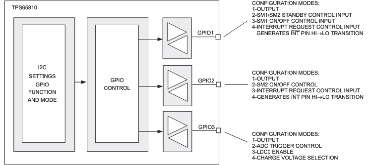 Figure 48. Required External Components, Recommended Values, External Connections
8.4 Device Functional Modes
8.4.1 Sleep Mode
The device enters the Sleep mode if a thermal fault or a system low voltage fault is detected. For a detailed description of which registers are reset to their default state and which registers keep their state, reference the section on System Sequencing and TPS65810 Operating Modes.
8.4.2 Normal Mode
The device enters the Normal mode after all power-good checks pass. In this mode, the I2C registers define the operation of the device.
8.5 Programming
8.5.1 Serial Interface
8.5.1.1 Overview
The TPS65810 device is compatible with a host-controlled environment, with internal parameters and status information accessible through an I2C interface. An I2C communication port provides a simple way for an
I2C-compatible host to access system status information and reset fault modes, functioning as a SLAVE port enabling I2C-compatible hosts to WRITE to or to READ from internal registers. The TPS65810 I2C port is a
2-wire bidirectional interface using SCL (clock) and SDA (data) pins; the SDA pin is open-drain and requires an external pullup. The I2C is designed to operate at SCL frequencies up to 400 kHz. The standard 8-bit command is supported, the CMD part of the sequence is the 8-bit register address to READ from or to WRITE to.
8.5.1.2 Register Default Values
The internal TPS65810 registers are loaded during the initial power-up from an internal, non-volatile memory bank. The power-up default values are described in the sections detailing the registers functionality.
The register contents remain intact as long as OUT pin voltage remains above the internal UVLO threshold, VUVLO. All register bits are reset to the internal power up default when the OUT pin voltage falls below the VUVLO threshold or if the HOT_RESET pin is set to LO.
8.5.1.3 I2C Address
The I2C specification contains several global addresses, which the slaves on the bus are required to respond to. The TPS65810 only responds (ACK) to addresses: 0x90 and 0x91 and does not respond (NACK) to any other address.
Table 27. TPS65810 I2C Read and Write Address
| BYTE | BIT | |||||||
|---|---|---|---|---|---|---|---|---|
| MSB | 6 | 5 | 4 | 3 | 2 | 1 | LSB | |
| TPS65810 I2C WRITE ADDRESS | 1 | 0 | 0 | 1 | 0 | 0 | 0 | 0 |
| TPS65810 I2C READ ADDRESS | 1 | 0 | 0 | 1 | 0 | 0 | 0 | 1 |
| I/O DATA BUS | B7 | B6 | B5 | B4 | B3 | B2 | B1 | B0 |
8.5.1.4 Incremental Read
The TPS65810 does not support incremental read operations. Each register must be accessed in a single read operation.
8.5.1.5 I2C Bus Release
The TPS65810 I2C engine does not create START or STOP states on the I2C bus during normal operation.
8.5.1.6 Sleep Mode Operation
When the sleep mode is set SDAT is held LO by the TPS65810. The overall system operation is not affected, as in sleep mode all TPS65810 integrated supplies are disabled and no power is available for any external devices connected to the TPS65810 SDAT pin. When sleep mode ends the SDAT pin is released before the TPS65810 integrated regulated supplies are enabled. See section on System Sequencing and TPS65810 Operating Modes for additional details on sleep mode operation.
8.5.1.7 I2C Communication Protocol
Table 28 lists the conventions used when describing the communication protocol.
Table 28. I2C Naming Conventions Used
| CONDITION | CODE |
|---|---|
| START sent from host | S |
| STOP sent from host | P |
| TPS65810 I2C slave address sent from host, bus direction set from host to TPS65810 (WRITE) | hA0 |
| TPS65810 register address sent from TPS65810, bus direction is from TPS65810 to host (READ) | hA1 |
| Non-valid I2C slave address sent from host | hA_N |
| Valid TPS65810 register address sent from host | HCMD |
| Non-valid TPS65810 register address sent from host | HCMD_N |
| I/O data byte (8 bits) sent from host to TPS65810 | hDATA |
| I/O data byte (8 bits) sent from TPS65810 to host | bqDATA |
| Acknowledge (ACK) from host | hA |
| Not acknowledge (NACK) from host | hN |
| Acknowledge (ACK) from TPS65810 | bqA |
| Not acknowledge (NACK) from TPS65810 | bqN |
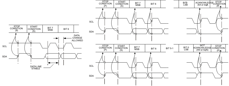 Figure 49. I2C operation waveforms
For normal data transfers, SDA is allowed to change only when SCL is low, and one clock pulse is used per bit of data. The SDA line must remain stable whenever the SCL line is high, as SDA changes when SCL is high are reserved for indicating the start and stop conditions. Each data transfer is initiated with a start condition and terminated with a stop condition.
When addressed, the TPS65810 device generates an acknowledge bit after the reception of each byte by pulling the SDA line Low. The master device (microprocessor) must generate an extra clock pulse that is associated with the acknowledge bit. After the acknowledge or not acknowledge bit, the TPS65810 device leaves the data line high, enabling a STOP condition generation.
8.5.1.8 I2C Read and Write Operations
The TPS65810 device supports the standard I2C one-byte Write. The basic I2C read protocol has the following steps:
- Host sends a start and sets TPS65810 I2C slave address in write mode
- The TPS65810 device acknowledges (ACKs) that this is a valid I2C address and that the bus is configured for write
- Host sends TPS65810 register address
- The TPS65810 device acknowledges (ACKs) that this is a valid register and stores the register address to be read
- Host sends a repeated start and TPS65810 I2C slave address, reconfiguring the bus for read
- The TPS65810 device acknowledges (ACKs) that this is a valid address and that bus is reconfigured
- Bus is in read mode, TPS65810 device begins sending data from selected register
The I2C write protocol is similar to the read, without the need for a repeated start and bus being set in write mode. In a WRITE, it is not necessary to end each 1-byte WRITE command with a STOP; a START has the same effect (repeated start).
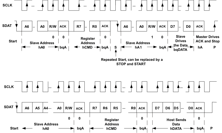 Figure 50. I2C read and write operations
The host can complete a READ or a WRITE sequence with either a STOP or a START.
8.5.1.9 Valid Write Sequences
The TPS65810 device always ACKs its own address. If the CMD points to an allowable READ or WRITE address, bq writes the address into its RAM address register and sends an ACK. If the CMD points to a
non-allowed address, bq does NOT write the address into its RAM address register and sends a NACK.
Table 1. Valid Write Sequence Address Registers
| S | hA0 | bqA | ||
| S | hA0 | bqA | hCMD | bqA |
| S | hA0 | bqA | hCMD_N | bqN |
8.5.1.10 One-Byte Write
The data is written to the addressed register when the bq ACK ending the one byte write sequence is received. The host can cancel a WRITE by sending a STOP or START before the trailing edge of the bq ACK clock pulse.
Table 2. One-Byte Write Address Register
| S | hA0 | bqA | hCMD | bqA | hDATA | bqA |
8.5.1.11 Valid Read Sequences
The TPS65810 always ACKs its own address.
Table 3. Valid Read Sequence ACK Register
| S | hA1 | bqA |
Upon receiving hA1, TPS65810 starts at wherever the RAM address register is pointing. The START and the STOP both act as priority interrupts. If the host has been interrupted and is not sure where it left off it can send a STOP and reset the TPS65810 state machine to the WAIT state; once in WAIT state, the TPS65810 ignores all activity on the SCL and SDA lines until it receives a START. A repeated START and START in the I2C specification are both treated as a START.
Table 4. Valid Read Sequence Address Registers
| S | hA0 | bqA | hCMD | bqA | P | |||||
| S | hA0 | bqA | hCMD | bqA | S | hA1 | bqA | bqDATA | hN | P |
| S | hA1 | bqA | bqDATA | hN | P | |||||
8.5.1.12 Non-Valid Sequences
Table 5. Incremental Read Sequences
| S | hA1 | bqA | bqDATA | hA | bqDATA | hA | bqDATA | hA | bqDATA | hA | ... | bqDATA | hA | P |
A START followed by an address which is not bqA0 or bqA1 is NACKED.
Table 6. START and Non-HA0 or Non-HA1 Address
| S | hA_N | bqN |
If the CMD points to a non-allowed READ address (reserved registers), bq sends a NACK back to the host, and it does not load the address in the RAM address register. Note that TPS65810 NACKS whether a stop is sent or not.
Table 7. Attempt to Specify Non-Allowed READ Address
| S | hA0 | bqA | hCMD_N | bqN | P |
| S | hA0 | bqA | hCMD_N | bqN |
If the host attempts to WRITE to a READ-ONLY or non-accessible address TPS65810 ACKS the CMD containing the allowed READ address, loads the address into the address register and NACKS after the host sends the next data byte. After issuing the NACK TPS65810 returns to WAIT state. A subsequent hA1 READ could read this address.
Table 8. Attempt to Specify Non-Allowed WRITE Address
| S | hA0 | bqA | hCMD | bqA | hDATA | bN |
8.6 Register Maps
Table 29. TPS65810 Internal Register Map
| Hex | Name | Description | Additional Details |
|---|---|---|---|
| 0 | RESERVED_01 | RESERVED | FACTORY ONLY |
| 1 | RESERVED_02 | RESERVED | FACTORY ONLY |
| 2 | PGOOD | Output voltage status for linear regulators and DC–DC buck converters | |
| 3 | INTMASK1 | Interrupt request masking settings | |
| 4 | INTMASK2 | Interrupt request masking settings | |
| 5 | INT_ACK1 | Masked interrupt request register, latched | |
| 6 | INT_ACK2 | Masked interrupt request register, latched | |
| 7 | PGOODFAULT_MASK | System Reset masking settings | |
| 8 | SOFT_RESET | Generates a software reset | |
| 9 | CHG_CONFIG | Battery charger configuration | |
| A | CHG_STAT | Battery charger status | |
| B | EN_LDO | Linear regulator ON/OFF control | |
| C | LDO12 | LDO1 and LDO2 output voltage setting | |
| D | LDO3 | LDO3 output voltage settings | |
| E | LDO4 | LDO4 output voltage settings | |
| F | LDO5 | LDO5 output voltage settings | |
| 10 | SM1_SET1 | SM1 Buck converter ON/OFF control and output voltage setting, normal mode | |
| 11 | SM1_SET2 | SM1 Buck converter configuration | |
| 12 | SM1_STANDBY | SM1 Buck converter stand-by mode ON/OFF and stand-by output voltage setting | |
| 13 | SM2_SET1 | SM2 Buck converter ON/OFF control and output voltage setting, normal mode | |
| 14 | SM2_SET2 | SM2 Buck converter configuration | |
| 15 | SM2_STANDBY | SM2 Buck converter stand-by mode ON/OFF and stand-by output voltage setting | |
| 16 | SM3_SET | SM3 White LED driver ON/OFF control and settings | |
| 17 | RGB_FLASH | Overall RGB driver timing settings | |
| 18 | RGB_RED | RGB driver: RED duty cycle and output current setting | |
| 19 | RGB_GREEN | RGB driver: GREEN duty cycle and output current setting | |
| 1A | RGB_BLUE | RGB driver: BLUE duty cycle and output current setting | |
| 1B | GPIO12 | GPIO1 and GPIO2 configuration | |
| 1C | GPIO3 | GPIO2 and GPIO3 configuration, battery charge voltage selection | |
| 1D | PWM | PWM output configuration | |
| 1E | ADC_SET | ADC On/OFF control, ADC configuration | |
| 1F | ADC reading_hi | ADC data output | |
| 20 | ADC reading_lo | ADC data output | |
| 21 | DHILIM1 | ADC Maximum threshold setting | |
| 22 | DHILIM2 | ADC Maximum threshold setting | |
| 23 | DLOLIM1 | ADC Minimum threshold setting | |
| 24 | DLOLIM2 | ADC Minimum threshold setting | |
| 25 | ADC_DELAY | ADC configuration: conversion delay | |
| 26 | ADC_WAIT | ADC configuration: wait and repeat operation | |
| 27 | LED_PWM | LED_PWM configuration | |
| 2E | RESERVED_03 | RESERVED | FACTORY ONLY |
8.6.1 Sequencing and Operating Modes – I2C Registers
The I2C registers that control sequencing-related functions are shown in Table 30. The HEX address for each register is shown by the register name, together with the R or W functionality for the register bits. Shaded values indicate default initial power-up values.
Table 30. I2C Registers – Sequencing and Operating Modes
| B7 | B6 | B5 | B4 | B3 | B2 | B1 | B0 | |
|---|---|---|---|---|---|---|---|---|
| Soft_reset, Address = 08, All Bits R/W, Bits B7/B6/B1/B0 Apply to Sequencing. | ||||||||
| Bit Name | STBY MODE | SLEEP MODE | NOT USED | NOT USED | SM3_LF_OSc | NOT USED | nRAMLOAD | SOFT RST |
| Function | SET SM1 AND SM2 IN STANDBY MODE | SET TPS65810 IN SLEEP MODE | NOT USED | NOT USED | NOT RELATED TO SEQUENCING See SM3 SECTION | NOT USED | RAM RESET FLAG | SOFTWARE RESET CONTROL |
| When 0 | NOT ACTIVE | NOT ACTIVE | NOT USED | NOT USED | NOT USED | RAM DEFAULTS LOADED | NOT ACTIVE | |
| When 1 | When 1 SET SM1 AND SM2 IN STANDBY | SET SLEEP MODE (reset to LO internally) | NOT USED | NOT USED | NOT USED | RAM DEFAULTS NOT LOADED | SET RESET MODE (reset to LO internally) | |
Some host algorithms need to identify when the power-up defaults are loaded in the RAM, to start routines that initialize specific RAM registers. If that functionality is required the nRAMLOAD bit must be set to HI by the host when entering the NORMAL operation mode. The nRAMLOAD bit is reset to LO by the TPS65810 when the power-up defaults are loaded in the I2C registers (V(OUT) < VUVLO OR V(HOT_RESET) = LO), enabling the host algorithm to detect that the RAM registers need to be initialized.
The integrated supplies status is available in a dedicated register, shown below. The host can select which integrated supply outputs trigger a power-good fault condition using the PGOODFAULT_MASK register. When a non-masked power-good status register bit toggles state, the sequence controller generates a transition in the TPS65810 state machine, indicated as a PGOOD FAULT in TPS65810 state diagram. The power-good status register and mask register are shown below:
Table 31. System Status Monitored By Sequencing Controller
| B7 | B6 | B5 | B4 | B3 | B2 | B1 | B0 | |
|---|---|---|---|---|---|---|---|---|
| PGOOD, Address = 02, All Bits Read Only - Power Up Defaults Show System Status When Exiting Power Down | ||||||||
| Bit name | PGOOD SM1 | PGOOD SM2 | PGOOD SM3 | PGOOD LDO1 | PGOOD LDO2 | PGOOD LDO3 | PGOOD LDO4 | PGOOD LDO5 |
| Function | SM1 OUTPUT STATUS | SM2 OUTPUT STATUS | SM3 OVP STATUS | LDO1 OUTPUT STATUS | LDO2 OUTPUT STATUS | LDO3 OUTPUT STATUS | LDO4 OUTPUT STATUS | LDO5 OUTPUT STATUS |
| When 0 | OK | OK | OK | OK | OK | OK | OK | OK |
| When 1 | FAULT | FAULT | FAULT | FAULT | FAULT | FAULT | FAULT | FAULT |
| PGOODFAULT_MASK, Address = 07, All Bits R/W | ||||||||
| Bit name | MASK_PSM1 | MASK_PSM2 | MASK_PSM3 | MASK_PLDO1 | MASK_PLDO2 | MASK_PLDO3 | MASK_PLDO4 | MASK_PLDO5 |
| Function | MASK PGOOD FAULT BY SM1 | MASK PGOOD FAULT BY SM2 | MASK PGOOD FAULT BY SM3 | MASK PGOOD FAULT BY LDO1 | MASK PGOOD FAULT BY LDO2 | MASK PGOOD FAULT BY LDO3 | MASK PGOOD FAULT BY LDO4 | MASK PGOOD FAULT BY LDO5 |
| When 0 | UNMASKED | UNMASKED | UNMASKED | UNMASKED | UNMASKED | UNMASKED | UNMASKED | UNMASKED |
| When 1 | MASKED | MASKED | MASKED | MASKED | MASKED | MASKED | MASKED | MASKED |
8.6.2 System Status — I2C Registers
The I2C registers that have system status data are shown below. The HEX address for each register is shown by the register name, together with the R or W functionality for the register bits. Those registers are valid, after an initial power up, when the TPS65810 enters the normal operation mode.
Table 32. System Status Monitored By Interrupt Controller
| B7 | B6 | B5 | B4 | B3 | B2 | B1 | B0 | |
|---|---|---|---|---|---|---|---|---|
| PGOOD, Address = 02, All Bits Read Only - Power Up Defaults Show System Status When Exiting Power Down | ||||||||
| Bit name | PGOOD SM1 | PGOOD SM2 | PGOOD SM3 | PGOOD LDO1 | PGOOD LDO2 | PGOOD LDO3 | PGOOD LDO4 | PGOOD LDO5 |
| Function | SM1 OUTPUT STATUS | SM2 OUTPUT STATUS | SM3 OVP STATUS | LDO1 OUTPUT STATUS | LDO2 OUTPUT STATUS | LDO3 OUTPUT STATUS | LDO4 OUTPUT STATUS | LDO5 OUTPUT STATUS |
| When 0 | OK | OK | OK | OK | OK | OK | OK | OK |
| When 1 | FAULT | FAULT | FAULT | FAULT | FAULT | FAULT | FAULT | FAULT |
| ADC STATUS | ||||||||
| REGISTER ADC_READING_HI, B7: CONVERSION COMPLETE; INTERNAL STATUS BITS (NO I2C REGISTER BIT AVAILABLE: INPUT OUT OF RANGE (HI OR LO), ANLG1 PIN IMPEDANCE TO AGND2 EXCEEDS 1 mΩ. See additional details in the Analog-to-Digital Converter section. |
||||||||
| OTHER SYSTEM STATUS: THERMAL FAULT DETECTED | ||||||||
8.6.3 Interrupt Controller – I2C Registers
The I2C registers that control an interrupt generation (INT: HI→LO) are shown below. The HEX address for each register is shown by the register name, together with the R or W functionality for the register bits. Shaded values indicate default initial power-up values.
Table 33. Interrupt and Power-Good Fault Managerment Register
| B7 | B6 | B5 | B4 | B3 | B2 | B1 | B0 | |
|---|---|---|---|---|---|---|---|---|
| INTMASK1, Address = 03, All Bits R/W | ||||||||
| Bit name | MASK_ISM1 | MASK_ISM2 | MASK_ISM3 | MASK_ILDO1 | MASK_ILDO2 | MASK_ILDO3 | MASK_ILDO4 | MASK_ILDO5 |
| Function | MASK INT by SM1 PGOOD FAULT | MASK INT by SM2 PGOOD FAULT | MASK INT by SM3 PGOOD FAULT | MASK INT by LDO1 PGOOD FAULT | MASK INT by LDO2 PGOOD FAULT | Mask INT by LDO3 PGOOD FAULT | MASK INT by LDO4 PGOOD FAULT | MASK INT by LDO5 PGOOD FAULT |
| When 0 | UNMASKED | UNMASKED | UNMASKED | UNMASKED | UNMASKED | UNMASKED | UNMASKED | UNMASKED |
| When 1 | MASKED | MASKED | MASKED | MASKED | MASKED | MASKED | MASKED | MASKED |
| INTMASK2, Address = 04, All Bits R/W | ||||||||
| Bit name | MASK_IADC | MASK_IANLG1 | MASK_IGPIO2 | MASK_IGPIO1 | MASK_ITHSHUT | MASK_ICHGST | MASK_IADC_HI | MASK_IADC_LO |
| Function | MASKS INT BY ADC END OF CONVERSION | MASKS INT BY ANLG1 HIGH IMPEDANCE | MASKS INT BY GPIO2 EDGE TRANSITION | MASKS INT BY GPIO1 EDGE TRANSITION | MASKS INT BY THERMAL FAULT | MASK INT BY CHG_STAT REGISTER BITS | MASK INT BY ADC INPUT ABOVE HI LIMIT | MASK INT BY ADC INPUT BELOW LO LIMIT |
| When 0 | UNMASKED | UNMASKED | UNMASKED | UNMASKED | UNMASKED | UNMASKED | UNMASKED | UNMASKED |
| When 1 | MASKED | MASKED | MASKED | MASKED | MASKED | MASKED | MASKED | MASKED |
| INT_ACK1, Address = 05, All Bits R/W | ||||||||
| Bit name | ACK_SM1 | ACK_SM2 | ACK_SM3 | ACK_LDO1 | ACK_LDO2 | ACK_LDO3 | ACK_LDO4 | ACK_LDO5 |
| Function | SM1 INT REQUEST | SM2 INT REQUEST | SM3 INT REQUEST | LDO1 INT REQUEST | LDO2 INT REQUEST | LDO3 INT REQUEST | LDO4 INT REQUEST | LDO5 INT REQUEST |
| When 0 | CLEAR FLAG | CLEAR FLAG | CLEAR FLAG | CLEAR FLAG | CLEAR FLAG | CLEAR FLAG | CLEAR FLAG | CLEAR FLAG |
| When 1 | SM1 PGOOD FAULT GENERATED INT | SM2 PGOOD FAULT GENERATED INT | SM3 OVP FAULT GENERATED INT | LDO1 PGOOD FAULT GENERATED INT | LDO2 PGOOD FAULT GENERATED INT | LDO3 PGOOD FAULT GENERATED INT | LDO4 PGOOD FAULT GENERATED INT | LDO5 PGOOD FAULT GENERATED INT |
| INT_ACK2, Address = 06, All Bits Read Only | ||||||||
| Bit name | ACK_ADC | ACK_ANLG1 | ACK_GPIO2 | ACK_GPIO1 | ACK_THSHUT | ACK_CHGSTAT | ACK_ADC_HI | ACK_ADC_LO |
| Function | ADC INT REQUEST 1 | ANLG1 COMPARATOR INT REQUEST | GPIO2 INT REQUEST | GPIO1 INT REQUEST | THERMAL FAULT INT REQUEST | CHARGER INT REQUEST | ADC INT REQUEST 2 | ADC INT REQUEST 3 |
| When 0 | CLEAR FLAG | CLEAR FLAG | CLEAR FLAG | CLEAR FLAG | CLEAR FLAG | CLEAR FLAG | CLEAR FLAG | CLEAR FLAG |
| When 1 | ADC DONE GENERATED INT REQUEST | ANLG1 HIGH IMPEDANCE DETECTION GENERATED INT REQUEST | GPIO2 EDGE GENERATED INT REQUEST | GPIO1 EDGE GENERATED INT REQUEST | THERMAL FAULT GENERATED INT REQUEST | CHARGER STATUS CHANGE GENERATED INT REQUEST | ADC INPUT ABOVE HI LIMIT GENERATED INT REQUEST | ADC INPUT BELOW LO LIMIT GENERATED INT REQUEST |
| PGOODFAULT_MASK, Address = 07, All Bits R/W | ||||||||
| Bit name | PGOOD SM1 | PGOOD SM2 | PGOOD SM3 | PGOOD LDO1 | PGOOD LDO2 | PGOOD LDO3 | PGOOD LDO4 | PGOOD LDO5 |
| Function | MASK PGOOD FAULT BY SM1 | MASK PGOOD FAULT BY SM2 | MASK PGOOD FAULT BY SM3 | MASK PGOOD FAULT BY LDO1 | MASK PGOOD FAULT BY LDO2 | MASK PGOOD FAULT BY LDO3 | MASK PGOOD FAULT BY LDO4 | MASK PGOOD FAULT BY LDO5 |
| When 0 | UNMASKED | UNMASKED | UNMASKED | UNMASKED | UNMASKED | UNMASKED | UNMASKED | UNMASKED |
| When 1 | MASKED | MASKED | MASKED | MASKED | MASKED | MASKED | MASKED | MASKED |
8.6.4 Charge and System Power Management — I2C Registers
The I2C registers that control charger and power path related functions are shown below. The HEX address for each register is shown by the register name, together with the R or W functionality for the register bits. Shaded values indicate default initial power-up values. Note that the CHG_STAT register contents are valid only when either AC or USB power are applied to the TPS65810. The output of linear regulator LDO_PM can be used as an indicator of external input power detection; if LDO_PM is in regulation the CHG_STAT register contents are valid.
Table 34. CHG_CONFIG Address
| B7 | B6 | B5 | B4 | B3 | B2 | B1 | B0 | |
|---|---|---|---|---|---|---|---|---|
| CHG_CONFIG, Address = 9, All Bits R/W | ||||||||
| Bit name | VCHG | CHGON | NOT USED | ISET1_1 | ISET1_0 | ISET2 | PSEL | CE(1) |
| Function | CHARGE VOLTAGE SELECTION | SUSPEND CHARGE | NOT USED | CHARGE CURRENT SCALING FACTOR | USB CURRENT LIMIT | SELECTED INPUT CURRENT LIMIT | SYSTEM POWER SELECTION | |
| When 0 | 4.36 V | CHARGE SUSPENDED | NOT USED | 00= 0.25 10=0.75 01= 0.5 11= 1 Note: Relative to charge current programmed by external ISET pin resistor. |
100 mA | USE USB CURRENT LIMIT | BATTERY TO SYSTEM | |
| When 1 | 4.20 V | CHARGE ON | NOT USED | 500 mA | INPUT CURRENT LIMIT SET TO MAXIMUM | INPUT POWER TO SYSTEM(1) | ||
Table 35. GPIO3 Address
| B7 | B6 | B5 | B4 | B3 | B2 | B1 | B0 | |
|---|---|---|---|---|---|---|---|---|
| GPIO3, Address = 1C, All Bits R/W(1) | ||||||||
| Bit name | GPIO3i/O | GPIO3_LEVEL | LDO0_ENABLE | CHARGE _VLTG | NOT USED | GPIO2 _INTSRC | GPIO1 _INTSRC | GPIO2 _SM2 |
| Function | See Table 23 | See Table 23 | See Table 23 | CHARGE VOLTAGE SELECTION SAFETY BIT | NOT USED | See Table 23 | Table 23 | See Table 23 |
| When 0 | 4.2 V | |||||||
| When 1 | 4.36 V | |||||||
Table 36. CHG_STAT Address
| B7 | B6 | B5 | B4 | B3 | B2 | B1 | B0 | |
|---|---|---|---|---|---|---|---|---|
| CHG_STAT, Address = A, All Bits Read Only– Power Up Defaults Show System Status When Exiting Power Down | ||||||||
| Bit name | BAT_STAT(1) (2) | INPUT _PWR | THDPPM_ON | ACPG(3) | USBPG(3) | STAT1 | STAT2 | INP_OV |
| Function | BATTERY SUPPLEMENT MODE STATUS | SELECTED INPUT POWER STATUS | THERMAL LOOP AND DPPM STATUS | AC INPUT POWER STATUS | USB INPUT POWER STATUS | CHARGE STATUS | AC OR USB INPUT OVP DETECTION | |
| When 0 | SUPPLEMENT MODE OFF | AC INPUT SELECTED | BOTH OFF | AC NOT DETECTED | USB NOT DETECTED | 00 = FAULT/SUSPEND/OFF 01 = CHARGE DONE 10 = FAST CHARGE ON 11 = PRECHARGE |
NO OVP | |
| When 1 | SUPPLEMENT MODE ON | USB INPUT SELECTED | DPPM ON OR THERMAL ON | AC DETECTED | USB DETECTED | OVP DETECTED | ||
8.6.5 Linear Regulators — I2C Registers
The I2C registers that control LDO-related functions are shown below. The HEX address for each register is shown by the register name, together with the R or W functionality for the register bits. Shaded values indicate default initial power-up values.
Table 37. Linear Regulators Registers
| B7 | B6 | B5 | B4 | B3 | B2 | B1 | B0 | |
|---|---|---|---|---|---|---|---|---|
| EN_LDO: Address = B, All Bits R/W | ||||||||
| Bit name | LDO1_EN | LDO2_EN | LDO3_EN | LDO4_EN | LDO5_EN | SIM_SET | SIM EN1 | RTC_EN |
| Function | LDO1…5 ON/OFF CONTROL | SIM LDO output voltage | SIM/RTC ON/OFF CONTROL | |||||
| When 0 | OFF | OFF | OFF | OFF | OFF | 2.5 V, ON | OFF | OFF |
| When 1 | ON | ON | ON | ON | ON | 1.8 V | ON | ON |
| LDO12: Address = C, All Bits R/W | ||||||||
| Bit name | LDO1_DISCH | LDO1_2 SET | LDO1_1 SET | LDO1_0 SET | LDO2_DISCH | LDO2_2 SET | LDO2_1 SET | LDO2_0 SET |
| Function | LDO1 output discharge switch enable | LDO1 OUTPUT VOLTAGE SETTING | LDO2 output discharge switch enable | LDO2 OUTPUT VOLTAGE SETTING | ||||
| When 0 | OFF | 000 = 1.25 V
010 = 1.8 V 100 = 2.85 V 110 = 3.2 V |
001 = 1.5 V 011 = 2.5 V 110 = 3 V 111 = 3.3 V |
Default =
1.25 V |
OFF | 000 = 1.25 V 010 = 1.8 V 100 = 2.85 V 110 = 3.2 V |
001 = 1.5 V 011 = 2.5 V 110 = 3 V 111 = 3.3 V |
Default = 3.3 V |
| When 1 | ON | ON | ||||||
| LDO3, Address = D, All Bits R/W | ||||||||
| Bit name | LDO3_DISCH | LDO3_6 SET | LDO3_5 SET | LDO3_4 SET | LDO3_3 SET | LDO3_2 SET | LDO3_1 SET | LDO3_0 SET |
| Function | LDO3 output discharge switch enable | LDO3 OUTPUT VOLTAGE SETTING | ||||||
| When 0 | OFF | See Table 38 for LDO3-5 output voltage setting, Power-up default = 1.505 V | ||||||
| When 1 | ON | |||||||
| LDO4, Address = E, All Bits R/W | ||||||||
| Bit name | LDO4_DISCH | LDO4_6 SET | LDO4_5 SET | LDO4_4 SET | LDO4_3 SET | LDO4_2 SET | LDO4_1 SET | LDO4_0 SET |
| Function | LDO4 output discharge switch enable | LDO4 OUTPUT VOLTAGE SETTING | ||||||
| When 0 | OFF | See Table 38 for LDO3-5 output voltage setting, Power-up default = 1.811 V | ||||||
| When 1 | ON | |||||||
| LDO5, Address = F, All Bits R/W | ||||||||
| Bit name | LDO5_DISCH | LDO5_6 SET | LDO5_5 SET | LDO5_4 SET | LDO5_3 SET | LDO5_2 SET | LDO5_1 SET | LDO5_0 SET |
| Function | LDO5 output discharge switch enable | LDO5 OUTPUT VOLTAGE SETTING | ||||||
| When 0 | OFF | See Table 38 for LDO3-5 output voltage setting, Power-up default = 3.111 V | ||||||
| When 1 | ON | |||||||
| GPIO3, Address = 1C, All Bits R/W. NOTE: ONLY BIT B5 CONTROLS LDO-RELATED FUNCTIONALITY | ||||||||
| Bit name | GPIO3i/O | GPIO3 LEVEL | LDO0 ENABLE | CHARGE _VLTG | NOT USED | GPIO2 _INTSRC | GPIO1 _INTSRC | GPIO2 _SM2 |
| Function | See Table 23 | See Table 23 | LDO0 ON/OFF CONTROL | See Table 23 | NOT USED | See Table 23 | See Table 23 | See Table 23 |
| When 0 | LDO0 OFF | |||||||
| When 1 | LDO0 ON | |||||||
Table 38. LDO 3–5 Programming Step Values
| Step | B6–B0 | Vset | Step | B6–B0 | Vset | Step | B6–B0 | Vset | Step | B6-B0 | Vset | |||
|---|---|---|---|---|---|---|---|---|---|---|---|---|---|---|
| 0 | 000 0000 | 1.224 | 32 | 010 0000 | 2.040 | 64 | 100 0000 | 2.015 | 96 | 110 0000 | 2.856 | |||
| 1 | 000 0001 | 1.250 | 33 | 010 0001 | 2.066 | 65 | 100 0001 | 2.040 | 97 | 110 0001 | 2.882 | |||
| 2 | 000 0010 | 1.275 | 34 | 010 0010 | 2.091 | 66 | 100 0010 | 2.907 | 98 | 110 0010 | 3.723 | |||
| 3 | 000 0011 | 1.301 | 35 | 010 0011 | 2.117 | 67 | 100 0011 | 2.933 | 99 | 110 0011 | 3.749 | |||
| 4 | 000 0100 | 1.326 | 36 | 010 0100 | 2.142 | 68 | 100 0100 | 2.958 | 100 | 110 0100 | 3.774 | |||
| 5 | 000 0101 | 1.352 | 37 | 010 0101 | 2.168 | 69 | 100 0101 | 2.984 | 101 | 110 0101 | 3.800 | |||
| 6 | 000 0110 | 1.377 | 38 | 010 0110 | 2.193 | 70 | 100 0110 | 3.009 | 102 | 110 0110 | 3.825 | |||
| 7 | 000 0111 | 1.403 | 39 | 010 0111 | 2.219 | 71 | 100 0111 | 3.035 | 103 | 110 0111 | 3.851 | |||
| 8 | 000 1000 | 1.428 | 40 | 010 1000 | 2.244 | 72 | 100 1000 | 3.060 | 104 | 110 1000 | 3.876 | |||
| 9 | 000 1001 | 1.454 | 41 | 010 1001 | 2.270 | 73 | 100 1001 | 3.086 | 105 | 110 1001 | 3.902 | |||
| 10 | 000 1010 | 1.479 | 42 | 010 1010 | 2.295 | 74 | 100 1010 | 3.111 | 106 | 110 1010 | 3.927 | |||
| 11 | 000 1011 | 1.505 | 43 | 010 1011 | 2.321 | 75 | 100 1011 | 3.137 | 107 | 110 1011 | 3.953 | |||
| 12 | 000 1100 | 1.530 | 44 | 010 1100 | 2.346 | 76 | 100 1100 | 3.162 | 108 | 110 1100 | 3.978 | |||
| 13 | 000 1101 | 1.556 | 45 | 010 1101 | 2.372 | 77 | 100 1101 | 3.188 | 109 | 110 1101 | 4.004 | |||
| 14 | 000 1110 | 1.581 | 46 | 010 1110 | 2.397 | 78 | 100 1110 | 3.213 | 110 | 110 1110 | 4.029 | |||
| 15 | 000 1111 | 1.607 | 47 | 010 1111 | 2.423 | 79 | 100 1111 | 3.239 | 111 | 110 1111 | 4.055 | |||
| 16 | 001 0000 | 1.632 | 48 | 011 0000 | 2.448 | 80 | 101 0000 | 3.264 | 112 | 111 0000 | 4.080 | |||
| 17 | 001 0001 | 1.658 | 49 | 011 0001 | 2.474 | 81 | 101 0001 | 3.290 | 113 | 111 0001 | 4.106 | |||
| 18 | 001 0010 | 1.683 | 50 | 011 0010 | 2.499 | 82 | 101 0010 | 3.315 | 114 | 111 0010 | 4.131 | |||
| 19 | 001 0011 | 1.709 | 51 | 011 0011 | 2.525 | 83 | 101 0011 | 3.341 | 115 | 111 0011 | 4.157 | |||
| 20 | 001 0100 | 1.734 | 52 | 011 0100 | 2.550 | 84 | 101 0100 | 3.366 | 116 | 111 0100 | 4.182 | |||
| 21 | 001 0101 | 1.760 | 53 | 011 0101 | 2.576 | 85 | 101 0101 | 3.392 | 117 | 111 0101 | 4.208 | |||
| 22 | 001 0110 | 1.785 | 54 | 011 0110 | 2.601 | 86 | 101 0110 | 3.417 | 118 | 111 0110 | 4.233 | |||
| 23 | 001 0111 | 1.811 | 55 | 011 0111 | 2.627 | 87 | 101 0111 | 3.443 | 119 | 111 0111 | 4.259 | |||
| 24 | 001 1000 | 1.836 | 56 | 011 1000 | 2.652 | 88 | 101 1000 | 3.468 | 120 | 111 1000 | 4.284 | |||
| 25 | 001 1001 | 1.862 | 57 | 011 1001 | 2.678 | 89 | 101 1001 | 3.494 | 121 | 111 1001 | 4.310 | |||
| 26 | 001 1010 | 1.887 | 58 | 011 1010 | 2.703 | 90 | 101 1010 | 3.519 | 122 | 111 1010 | 4.335 | |||
| 27 | 001 1011 | 1.913 | 59 | 011 1011 | 2.729 | 91 | 101 1011 | 3.545 | 123 | 111 1011 | 4.361 | |||
| 28 | 001 1100 | 1.938 | 60 | 011 1100 | 2.754 | 92 | 101 1100 | 3.570 | 124 | 111 1100 | 4.386 | |||
| 29 | 001 1101 | 1.964 | 61 | 011 1101 | 2.780 | 93 | 101 1101 | 3.596 | 125 | 111 1101 | 4.412 | |||
| 30 | 001 1110 | 1.989 | 62 | 011 1110 | 2.805 | 94 | 101 1110 | 3.621 | 126 | 111 1110 | 4.437 | |||
| 31 | 001 1111 | 2.015 | 63 | 011 1111 | 2.831 | 95 | 101 1111 | 3.647 | 127 | 111 1111 | 4.463 |
8.6.6 Switched-Mode Step-Down Converters — I2C Registers
The I2C registers that control buck converter-related functions are shown below. The HEX address for each register is shown by the register name, together with the R or W functionality for the register bits. Shaded values indicate default initial power-up values.
Table 39. Switched-Mode Step-Down Converters Registers
| B7 | B6 | B5 | B4 | B3 | B2 | B1 | B0 | |
|---|---|---|---|---|---|---|---|---|
| SM1_SET1, Address = 10, All Bits R/W | ||||||||
| Bit name | SM1 EN | PFM_RPL1 | PFM_SM1 | SetV4_SM1 | SetV3_SM1 | SetV2_SM1 | SetV1_SM1 | SetV0_SM1 |
| Function | SM1 ON/OFF CONTROL | SM1 PFM FUNCTION OPERATION | SM1 PFM MODE ON/OFF CTRL | SM1 OUTPUT VOLTAGE REGULATION VALUE, STANDBY MODE NOT SET | ||||
| When 0 | OFF | MAXIMIZE EFFICIENCY | PWM/PFM | See Table 40 for SM1, SM2 voltage setting, Power up default=1.24 V | ||||
| When 1 | ON | MINIMIZE OUTPUT RIPPLE | Only PWM | |||||
| SM1_SET2, Address = 11, All Bits R/W | ||||||||
| Bit name | NOT USED | STANDBY_SM1 | DISCHSM1 | S1S2PHASE_1 | S1S2PHASE_0 | SLEWSM1_2 | SLEWSM1_1 | SLEWSM1_0 |
| Function | NOT USED | SM1 STANDBY MODE ON | SM1 output discharge switch enable | SM2 PWM CLOCK DELAY, WITH RESPECT TO SM1 PWM CLOCK | SM1 OUTPUT SLEW RATE SETTING | |||
| When 0 | NOT USED | OFF | OFF | 00 = 0° 01 = 90° |
10 = 180°
11 = 270° Default = 180° |
000 = 0.24 010 = 0.96 100 = 5.84 110 = 15.36
001 = 0.48 011 = 1.92 101 = 7.68 111 = IMMEDIATE Unit: mV/μs Default= 15.36 |
||
| When 1 | NOT USED | ON | ON |
|||||
| SM1_STANDBY, Address = 12, B4-B0 R/W, B7-B5 Read Only | ||||||||
| Bit name | GPIO3LVL | GPIO2LVL | GPIO1LVL | SetV4_SM1SL | SetV3_SM1SL | SetV2_SM1SL | SetV1_SM1SL | SetV0_SM1SL |
| Function | GPIO3 pin logic level | GPIO2 pin logic level | GPIO1 pin logic level | SM1 OUTPUT VOLTAGE REGULATION VALUE, STANDBY MODE SET | ||||
| When 0 | LO | LO | LO | See Table 40 for SM1, SM2 voltage setting, Power-up default = 1.24 V | ||||
| When 1 | HI | HI | HI | |||||
| SM2_SET1, Address = 13, All Register Bits R/W | ||||||||
| Bit name | SM2 EN | PFM_RPL2 | PFM_SM2 | SetV4_SM2 | SetV3_SM2 | SetV2_SM2 | SetV1_SM2 | SetV0_SM2 |
| Function | SM2 ON/OFF CONTROL | SM2 PFM FUNCTION OPERATION | SM2 PFM MODE ON/OFF CTRL | SM2 OUTPUT VOLTAGE REGULATION VALUE, STANDBY MODE NOT SET | ||||
| When 0 | OFF | MAXIMIZE EFFICIENCY | PWM/PFM | See Table 40 for SM1, SM2 voltage setting, Power-up default = 3.32 V | ||||
| When 1 | ON | MINIMIZE OUTPUT RIPPLE | ONLY PWM | |||||
| SM2_SET2, Address = 14, All Register Bits R/W | ||||||||
| Bit name | NOT USED | STANDBY_SM2 | DISCHSM2 | NOT USED | NOT USED | SLEWSM2_2 | SLEWSM2_1 | SLEWSM2_0 |
| Function | NOT USED | SM2 STANDBY MODE ON | SM2 output discharge switch enable | NOT USED | NOT USED | SM2 OUTPUT SLEW RATE SETTING | ||
| When 0 | NOT USED | OFF | OFF | NOT USED | NOT USED | 000 = 0.48 010 = 1.92 100 = 7.68 110 = 30.72 001 = 0.096 011 = 3.84 101 = 15.36 111 = IMMEDIATE Unit: mV/μs Default = 30.72 |
||
| When 1 | NOT USED | ON | ON | NOT USED | NOT USED | |||
| SM2_STANDBY, Address = 15, All Register Bits R/W | ||||||||
| Bit name | NOT USED | NOT USED | NOT USED | SetV4_SM2SL | SetV3_SM2SL | SetV2_SM2SL | SetV1_SM2SL | SetV0_SM2SL |
| Function | NOT USED | NOT USED | NOT USED | SM1 OUTPUT VOLTAGE REGULATION VALUE, STANDBY MODE SET | ||||
| When 0 | NOT USED | NOT USED | NOT USED | See Table 40 for SM1, SM2 voltage setting, Power up default=3.32 V | ||||
| When 1 | NOT USED | NOT USED | NOT USED | |||||
Table 40. Programmable Settings for SM1 and SM2 (Including STANDBY)
| SetV4_ SM | SetV3_ SM | SetV2_ SM | SetV1_ SM | SetV0_ SM | Vset SM1 | Vset SM2 | SetV4_ SM | SetV3_ SM | SetV2_ SM | SetV1_ SM | SetV0_ SM | Vset SM1 | Vset SM2 | |
|---|---|---|---|---|---|---|---|---|---|---|---|---|---|---|
| 0 | 0 | 0 | 0 | 0 | 0.6 | 1 | 1 | 0 | 0 | 0 | 0 | 1.24 | 2.28 | |
| 0 | 0 | 0 | 0 | 1 | 0.64 | 1.08 | 1 | 0 | 0 | 0 | 1 | 1.28 | 2.36 | |
| 0 | 0 | 0 | 1 | 0 | 0.68 | 1.16 | 1 | 0 | 0 | 1 | 0 | 1.32 | 2.44 | |
| 0 | 0 | 0 | 1 | 1 | 0.72 | 1.24 | 1 | 0 | 0 | 1 | 1 | 1.36 | 2.52 | |
| 0 | 0 | 1 | 0 | 0 | 0.76 | 1.32 | 1 | 0 | 1 | 0 | 0 | 1.4 | 2.6 | |
| 0 | 0 | 1 | 0 | 1 | 0.8 | 1.4 | 1 | 0 | 1 | 0 | 1 | 1.44 | 2.68 | |
| 0 | 0 | 1 | 1 | 0 | 0.84 | 1.48 | 1 | 0 | 1 | 1 | 0 | 1.48 | 2.76 | |
| 0 | 0 | 1 | 1 | 1 | 0.88 | 1.56 | 1 | 0 | 1 | 1 | 1 | 1.52 | 2.84 | |
| 0 | 1 | 0 | 0 | 0 | 0.92 | 1.64 | 1 | 1 | 0 | 0 | 0 | 1.56 | 2.92 | |
| 0 | 1 | 0 | 0 | 1 | 0.96 | 1.72 | 1 | 1 | 0 | 0 | 1 | 1.6 | 3 | |
| 0 | 1 | 0 | 1 | 0 | 1 | 1.8 | 1 | 1 | 0 | 1 | 0 | 1.64 | 3.08 | |
| 0 | 1 | 0 | 1 | 1 | 1.04 | 1.88 | 1 | 1 | 0 | 1 | 1 | 1.68 | 3.16 | |
| 0 | 1 | 1 | 0 | 0 | 1.08 | 1.96 | 1 | 1 | 1 | 0 | 0 | 1.72 | 3.24 | |
| 0 | 1 | 1 | 0 | 1 | 1.12 | 2.04 | 1 | 1 | 1 | 0 | 1 | 1.76 | 3.32 | |
| 0 | 1 | 1 | 1 | 0 | 1.16 | 2.12 | 1 | 1 | 1 | 1 | 0 | 1.8 | 3.4 | |
| 0 | 1 | 1 | 1 | 1 | 1.2 | 2.2 | 1 | 1 | 1 | 1 | 1 | 0.6 | 1 |
Table 41. Programmable Settings for SM1 and SM2 Phase and Slew Rate
| SM1, SM2 PHASE | SMX_SLEW RATE, SMX = SM1 OR SM2 | |||||||
|---|---|---|---|---|---|---|---|---|
| S1S2_PHASE1 | S1S2_PHASE0 | PHASE | SLEWX_2 | SLEWX_1 | SLEWX_0 | SM1
mV/μs |
SM2
mV/μs |
|
| 0 | 0 | 0° | 0 | 0 | 0 | 0.24 | 0.48 | |
| 0 | 1 | 90° | 0 | 0 | 1 | 0.48 | 0.96 | |
| 1 | 0 | 180° | 0 | 1 | 0 | 0.96 | 1.92 | |
| 1 | 1 | 270° | 0 | 1 | 1 | 1.92 | 3.84 | |
| 1 | 0 | 0 | 3.84 | 7.68 | ||||
| 1 | 0 | 1 | 7.68 | 15.36 | ||||
| 1 | 1 | 0 | 15.36 | 30.72 | ||||
| 1 | 1 | 1 | Immediate | |||||
8.6.7 ADC – I2C Registers
The I2C registers that control ADC-related functions are shown below. The HEX address for each register is shown by the register name, together with the R or W functionality for the register bits. Default, initial power-up values are shown in bold. In the timing equations, replace Bn with 1 for HI state, and 0 for LO state.
Table 42. ADC Registers
| B7 | B6 | B5 | B4 | B3 | B2 | B1 | B0 | |
|---|---|---|---|---|---|---|---|---|
| ADC_SET, Address = 1E, All Bits R/W | ||||||||
| Bit Name | ADC_ENABLE | ADC_REF_EN | CHSEL2_SET | CHSEL1_SET | CHSEL0_SET | READ_MODE2 | READ_MODE1 | READ_MODE0 |
| Function | ADC ON/OFF CONTROL | ADC REFERENCE SELECTION | ADC CHANNEL SELECTION | ADC SAMPLING SETTINGS | ||||
| When 0 | OFF | Internal | 000 = ANLG1
001 = ANLG2 010 = V(ISET1) |
011 = V(TS) 100 = Tj 101 = V(RTC_OUT) |
110 = V(OUT) 111 = V(BAT) Default = ANLG1 |
000 = 1
001= 4 010 = 8 |
011 = 16 100 = 32 101 = 64 |
110 = 128 111 = 256 Default = 1 |
| When 1 | ON | External | ||||||
| ADC READING_HI, Address = 1F, Bits B3/B4 R/W, All Other Bits Read Only | ||||||||
| Bit Name | ADC_STATUS | NOT USED | NOT USED | ADC_READ1 | ADC_READ0 | D10 | D9_MSB | D8 |
| Function | CURRENT CONVERSION STATUS | NOT USED | NOT USED | ALU OUTPUT DATA SELECTION | ADC AVERAGE CARRYOVER BIT | ADC CONVERSION OUTPUT BITS | ||
| When 0 | DONE | NOT USED | NOT USED | 00=LAST 10 = MAXIMUM 01=AVERAGE 11 = MINIMUM Default= LAST |
VALID ONLY AFTER ADC CONVERSION ENDS SEE ADC_READING_LO | |||
| When 1 | BUSY | NOT USED | NOT USED | |||||
| ADC READING_LO, Address = 20, Read Only | ||||||||
| Bit Name | D7 | D6 | D5 | D4 | D3 | D2 | D1 | D0_LSB |
| Function | ADC CONVERSION OUTPUT BITS, VALID ONLY AFTER ADC CONVERSION ENDS | |||||||
| Value | VALUE=[B10*512 + B9*256 + B8*128 + B7*64 + B6*32 + B5*16 + B4*8 + B3*4 + B2*2 + B1] * [ VRNG(CHn) / 1023]; Unit=Volts, The LSB bit value is proportional to the ADC reference voltage - See VRNG(CHn) in electrical parameters |
|||||||
| DHILIM1, Address = 21, All Bits R/W | ||||||||
| Bit Name | NOT USED | NOT USED | NOT USED | NOT USED | NOT USED | DHILIM10 | DHILIM9 | DHILIM8 |
| Function | RESERVED | ADC MAX INPUT LIMIT RANGE SETTING (3 MSBs) | ||||||
| DHILIM2, Address = 22, All Bits R/W | ||||||||
| Bit Name | DHILIM7 | DHILIM6 | DHILIM5 | DHILIM4 | DHILIM3 | DHILIM2 | DHILIM1 | DHILIM0_LSB |
| Function | ADC MAX INPUT LIMIT RANGE SETTING (8 LSBs) | |||||||
| DLOLIM1, Address = 23, All Bits R/W | ||||||||
| Bit Name | NOT USED | NOT USED | NOT USED | NOT USED | NOT USED | DLOLIM10 | DLOLIM9 | DLOLIM8 |
| Function | RESERVED | ADC MIN INPUT LIMIT RANGE SETTING (3 MSBs) | ||||||
| DLOLIM2, Address = 24, All Bits R/W | ||||||||
| Bit Name | DLOLIM7 | DLOLIM6 | DLOLIM5 | DLOLIM4 | DLOLIM3 | DLOLIM2 | DLOLIM1 | DLOLIM0_LSB |
| Function | ADC MIN INPUT LIMIT RANGE SETTING (8 LSBs) | |||||||
| ADC_DELAY, Address = 25, All Bits R/W | ||||||||
| Bit Name | ADC_TRG_GPIO3 | EDGE _GPIO3 | HOLDOFF | REPEAT | Delay_3 | Delay_2 | Delay_1 | Delay_0 |
| Function | USE GPIO3 AS ADC TRIGGER | GPIO3 TRIGGER MODE | ADC HOLDOFF ON/OFF CONTROL | REPEAT MODE ON/OFF | ADC EXTERNAL TRIGGER DELAY SETTING | |||
| When 0 | OFF | Falling Edge | OFF | OFF | tDLY(TRIG)= B4*400 + B3 * 200 + B2*100 + B1* 50, Units = μs Default = 0 μs | |||
| When 1 | ON | Rising Edge | ON | ON | ||||
| ADC_WAIT, Address = 26, All Bits R/W | ||||||||
| Bit Name | ADC_cH2I_D1 | ADC_cH2I_D0 | BATIDI_D1 | BATIDI_D0 | WAIT_D3 | WAIT_D2 | WAIT_D1 | WAIT_LSB |
| Function | ANLG2 PULL-UP CURRENT SOURCE VALUE | ANLG1 PULL-UP CURRENT SOURCE VALUE | ADC SAMPLE WAIT TIME, MULTIPLE SAMPLES MODE | |||||
| When 0 | 11:60 μA, 10:50 μA, 01:10 μA,00: 0
Default= 00 |
11:60 μA, 10:50 μA, 01:10 μA, 00: WEAK PULL UP Default: 00 |
0000 = 0
0001 = 0.02 0010 = 0.04 0011 = 0.06 Units = ms |
0100 = 0.08 0101 = 0.16 0110 = 0.24 0111 = 0.32 |
1000 = 0.64 1001 = 1.28 1010 = 1.92 1011 = 2.56 |
1100 = 5.12 1101 = 10.24 1110 = 15.36 1111 = 20.48 Default = 0 |
||
| When 1 | ||||||||
8.6.8 White LED, PWM Drivers — I2C Registers
The I2C registers that control LED AND PWM driver related functions are shown below. The HEX address for each register is shown by the register name, together with the R or W functionality for the register bits. Shaded values indicate default initial power-up values. In the equations replace Bn with 1 for HI state, and 0 for LO state.
Table 43. White LED, PWM Drivers Registers
| B7 | B6 | B5 | B4 | B3 | B2 | B1 | B0 | |
|---|---|---|---|---|---|---|---|---|
| SM3_SET, Address = 16, All Bits R/W | ||||||||
| Bit Name | SM3_I7 set | SM3_I6 set | SM3_I5 set | SM3_I4 set | SM3_I3 set | SM3_I2 set | SM3_I1 set | SM3_I0 set |
| Function | SM3 DUTY CYCLE CONTROL | |||||||
| Value | See Table 19 for SM3 duty cycle settings, default = 0 (OFF) | |||||||
| RGB_FLASH, Address = 17, All Bits R/W | ||||||||
| Bit Name | FLASH_EN | FLASH_ON2 | FLASH_ON1 | FLASH_ON0 | FLASH_PER3 | FLASH_PER2 | FLASH_PER1 | FLASH_PER0 |
| Function | FLASH MODE ON/OFF CTRL | FLASH MODE ON TIME | FLASH MODE PERIOD | |||||
| When 0 | OFF | See Table 20 for RGB ON TIME settings, default = 0.1 | See Table 20 for RGB FLASH settings, default = 1 | |||||
| When 1 | ON | |||||||
| RGB_RED, Address = 18, All Bits R/W | ||||||||
| Bit Name | RGB_ISET1 | RGB_ISET0 | PHASE | PWMR_D4 | PWMR_D3 | PWMR_D2 | PWMR_D1 | PWMR_D0 |
| Function | RGB LED CURRENT SETTINGS | PHASE CONTROL | REG DRIVER DUTY CYCLE CONTROL | |||||
| When 0 | 00= 0 10= 8 mA 01= 4 mA 11=12 mA |
GREEN out of Φ with RED & BLUE | See Table 20 for RGB_RED DUTY settings, default = 0 | |||||
| When 1 | BLUE out of Φ with RED & GREEN | |||||||
| RGB_GREEN, Address = 19, All Bits R/W | ||||||||
| Bit Name | NOT USED | NOT USED | NOT USED | PWMG_D4 | PWMG_D3 | PWMG_D2 | PWMG_D1 | PWMG_D0 |
| Function | NOT USED | NOT USED | NOT USED | GREEN DRIVER DUTY CYCLE CONTROL | ||||
| Value | NOT USED | NOT USED | NOT USED | See Table 20 for RGB_GREEN DUTY settings, default = 0 | ||||
| RGB_BLUE, Address = 1A, All Bits R/W | ||||||||
| Bit Name | NOT USED | NOT USED | NOT USED | PWMB_D4 | PWMB_D3 | PWMB_D2 | PWMB_D1 | PWMB_D0 |
| Function | NOT USED | NOT USED | NOT USED | BLUE DRIVER DUTY CYCLE CONTROL | ||||
| Value | NOT USED | NOT USED | NOT USED | See Table 20 for RGB_BLUE DUTY settings, default = 0 | ||||
| PWM, Address = 1D, All Bits R/W | ||||||||
| Bit Name | PWM_EN | PWM1_F2 | PWM_F1 | PWM_F0 | PWM_D3 | PWM_D2 | PWM_D1 | PWM_D0 |
| Function | PWM ON/OFF CONTROL | PWM DRIVER FREQUENCY SETTINGS | PWM DRIVER DUTY CYCLE SETTINGS | |||||
| When 0 | Disabled | 000 = 15.6 kHz
001 = 7.8 kHz 010 = 4.5 kHz |
011 = 3 kHz 100 = 2 kHz 101 = 1.5 kHz |
110 = 1 kHz 111 = 500 Hz Default = 15.6 kHz |
See Table 21 for PWM DUTY settings, default = 0.0625 | |||
| When 1 | Enabled | |||||||
| LED_PWM, Address = 27, All Bits R/W | ||||||||
| Bit Name | LPWM_7 set | LPWM_6 set | LPWM_5 set | LPWM_4 set | LPWM_3 set | LPWM_2 set | LPWM_1 set | LPWM_0 set |
| Function | LED_PWM DRIVER DUTY CYCLE CONTROL | |||||||
| Value | See Table 19 for LED_PWM DUTY settings, default = 0 (OFF) | |||||||
8.6.9 GPIOs — I2C Registers
The I2C registers that control GPIO-related functions are shown below. The HEX address for each register is shown by the register name, together with the R or W functionality for the register bits. Shaded values indicate default initial power-up values.
Table 44. GPIOs Registers
| B7 | B6 | B5 | B4 | B3 | B2 | B1 | B0 | |
|---|---|---|---|---|---|---|---|---|
| GPIO12, Address = 1B, All Bits R/W | ||||||||
| Bit Name | GPIO2I/O | GPIO1I/O | GPIO2OUT | GPIO1OUT | GPIO2LVL | GPIO1LVL | GPIO1SMSBY | GPIO1SM1 |
| Function | GPIO2 MODE | GPIO1 MODE | SET GPIO2 LEVEL (OUTPUT ONLY) | SET GPIO1 LEVEL (OUTPUT ONLY) | GPIO2 EDGE AND LEVEL DETECTION | GPIO1 EDGE AND LEVEL DETECTION | GPIO 1 CONTROLS SM1 AND SM2 STANDBY ON/OFF | GPIO1 CONTROLS SM1 ON/OFF |
| When 0 | INPUT | INPUT | LOW | LOW | RISING EDGE, LO LEVEL | RISING EDGE, LO LEVEL | DISABLED | DISABLED |
| When 1 | OUTPUT | OUTPUT | HIGH | HIGH | FALLING EDGE, HI LEVEL | FALLING EDGE, HI LEVEL | ENABLED | ENABLED |
| GPIO3, Address = 1C, All Bits R/W | ||||||||
| Bit Name | GPIO3I/O | GPIO3OUT | LDO0_EN | CHG_VOLT | NOT USED | GPIO2 INT | GPIO1 INT | GPIO2SM2 |
| Function | GPIO3 MODE | SET GPIO3 LEVEL (OUTPUT ONLY) | LDO0 ON/OFF CONTROL | CHARGE VOLTAGE SAFETY BIT | NOT USED | GPIO2 TRIGGERS INT:HI→LO | GPIO1 TRIGGERS INT:HI→LO | SM2 ON/OFF CONTROL |
| When 0 | INPUT | LOW | OFF | 4.20 V | NOT USED | DISABLED | DISABLED | DISABLED |
| When 1 | OUTPUT | HIGH | ON | 4.36 V | NOT USED | ENABLED | ENABLED | ENABLED |