SWCS032F October 2008 – July 2014 TPS65950
PRODUCTION DATA.
- 1Device Overview
- 2Revision History
- 3Terminal Configuration and Functions
- 4Specifications
-
5Detailed Description
- 5.1
Power Module
- 5.1.1
Power Providers
- 5.1.1.1 VDD1 DC-DC Regulator
- 5.1.1.2 VDD2 DC-DC Regulator
- 5.1.1.3 VIO DC-DC Regulator
- 5.1.1.4 VDAC LDO Regulator
- 5.1.1.5 VPLL1 LDO Regulator
- 5.1.1.6 VPLL2 LDO Regulator
- 5.1.1.7 VMMC1 LDO Regulator
- 5.1.1.8 VMMC2 LDO Regulator
- 5.1.1.9 VSIM LDO Regulator
- 5.1.1.10 VAUX1 LDO Regulator
- 5.1.1.11 VAUX2 LDO Regulator
- 5.1.1.12 VAUX3 LDO Regulator
- 5.1.1.13 VAUX4 LDO Regulator
- 5.1.1.14 Internal LDOs
- 5.1.1.15 CP
- 5.1.1.16 USB LDO Short-Circuit Protection Scheme
- 5.1.2 Power References
- 5.1.3 Power Control
- 5.1.4 Power Consumption
- 5.1.5 Power Management
- 5.1.1
Power Providers
- 5.2 Real-Time Clock and Embedded Power Controller
- 5.3
Audio/Voice Module
- 5.3.1 Audio/Voice Downlink (RX) Module
- 5.3.2
Audio/Voice Uplink (TX) Module
- 5.3.2.1 Microphone Bias Module
- 5.3.2.2 Stereo Differential Input
- 5.3.2.3 Headset Differential Input
- 5.3.2.4 FM Radio/Auxiliary Stereo Input
- 5.3.2.5 PDM Interface for Digital Microphones
- 5.3.2.6 Uplink Characteristics
- 5.3.2.7 Microphone Amplification Stage
- 5.3.2.8 Carkit Input
- 5.3.2.9 Digital Audio Filter Module
- 5.3.2.10 Digital Voice Filter Module
- 5.4
USB HS 2.0 OTG Transceiver
- 5.4.1 USB Features
- 5.4.2
USB Transceiver
- 5.4.2.1 MCPC Carkit Port Timing
- 5.4.2.2 USB-CEA Carkit Port Timing
- 5.4.2.3 HS USB Port Timing
- 5.4.2.4
PHY Electrical Characteristics
- 5.4.2.4.1 5-V Tolerance
- 5.4.2.4.2 LS/FS Single-Ended Receivers
- 5.4.2.4.3 LS/FS Differential Receiver
- 5.4.2.4.4 LS/FS Differential Transmitter
- 5.4.2.4.5 HS Differential Receiver
- 5.4.2.4.6 HS Differential Transmitter
- 5.4.2.4.7 CEA/MCPC/UART Driver
- 5.4.2.4.8 Pullup/Pulldown Resistors
- 5.4.2.4.9 PHY DPLL Electrical Characteristics
- 5.4.2.4.10 PHY Power Consumption
- 5.4.2.5 OTG Electrical Characteristics
- 5.5 Battery Interface
- 5.6 MADC
- 5.7 LED Drivers
- 5.8 Keyboard
- 5.9 Clock Specifications
- 5.10 Debouncing Time
- 5.11 External Components
- 5.1
Power Module
- 6Device and Documentation Support
パッケージ・オプション
デバイスごとのパッケージ図は、PDF版データシートをご参照ください。
メカニカル・データ(パッケージ|ピン)
- ZXN|209
サーマルパッド・メカニカル・データ
発注情報
1 Device Overview
1.1 Features
- Power:
- Three Efficient Step-down Converters
- VDD1: TPS65950A2 with 1.2 A and TPS65950A3 with 1.4 A (for 1-GHz Speed)
- VDD2: 600 mA
- VIO: 700 mA
- 10 External Linear LDOs for Clocks and Peripherals
- SmartReflex™ Dynamic Voltage Management
- Three Efficient Step-down Converters
- Audio:
- Voice Codec
- 15-Bit Linear Codec (8 and 16 kHz)
- Differential Input Main and Submicrophones
- Differential Headset Microphone Input
- Auxiliary/FM Input (Mono or Stereo)
- Differential 32-Ω Speaker and 16-Ω Headset Drivers (External Predrivers for Class D)
- 8-Ω Stereo Class-D Drivers
- Pulse Code Modulation (PCM) and TDM Interfaces
- Bluetooth® Interface
- Automatic Level Control (ALC)
- Digital and Analog Mixing
- 16-Bit Linear Audio Stereo DAC (96, 48, 44.1, and 32 kHz, and Derivatives)
- 16-Bit Linear Audio Stereo ADC (48, 44.1, and 32 kHz, and Derivatives)
- Digital Microphone Inputs
- Carkit
- Charger:
- Li-ion, Li-on Polymer, and Cobalt-Nickel-Manganese Charger
- Supports Charging with AC-Regulated Charger (Maximum 7 V), USB Host Devices, Mobile Computing Promotion Consortium (MCPC) Devices, USB Chargers, and Carkit Chargers (Maximum 7 V)
- Backup Battery Charger
- USB:
- USB 2.0 OTG-Compliant HS Transceivers
- 12-Bit ULPI
- USB Power Supply (5-V CP for VBUS)
- CEA-2011: OTG Transceiver Interface Specification
- CEA-936A: Mini-USB Analog Carkit Interface Specification
- MCPC ME-Universal Asynchronous Receiver/Transmitter (UART) GL-006 Specification
- Additional Features:
- LED Driver Circuit for Two External LEDs
- 10-Bit MADC with 3 to 8 External Inputs
- RTC and Retention Modules
- HS Inter-Integrated Circuit (I2C) Serial Control
- Thermal Shutdown and Hot-Die Detection
- Keypad Interface (up to 8 × 8)
- External Vibrator (Vibrator) Control
- 19 GPIO Devices
- 0.4-mm Pitch, 209 Pin, 7-mm × 7-mm Package
1.3 Description
The TPS65950 device is a highly integrated power-management and audio coder/decoder (codec) integrated circuit (IC) that supports the power and peripheral requirements of the OMAP™ application processors. The device contains power management, an audio codec, a universal serial bus (USB) high-speed (HS) transceiver, an AC/USB charger, light-emitting diode (LED) drivers, an analog-to-digital converter (ADC), a real-time clock (RTC), and embedded power control.
The power portion of the device contains three buck converters, two controllable by a dedicated SmartReflex class-3 interface, multiple low-dropout (LDO) regulators, an embedded power controller (EPC) to manage the power-sequencing requirements of OMAP, and an RTC and backup module. The RTC can be powered by a backup battery when the main supply is not present, and the device contains a coin-cell charger to recharge the backup battery as needed.
The USB module provides a HS 2.0 on-the-go (OTG) transceiver suitable for direct connection to the OMAP universal transceiver macrocell interface (UTMI) + low pin interface (ULPI) with an integrated charge pump (CP) and full support for the carkit Consumer Electronics Association (CEA)-936A specification.
The Li-ion battery charger supports charging from AC chargers, USB host devices, USB chargers, or carkits. The device automatically detects the type of charger and provides hardware-controlled linear charging with AC chargers, USB chargers, and carkits, in addition to software-controlled charging for all charger types.
The audio codec in the device includes five digital-to-analog converters (DACs) and two ADCs to provide multiple voice channels and stereo downlink channels that can support all standard audio sample rates through several inter-IC sound (I2S)/time division multiplexing (TDM) format interfaces. The audio output stages on the device include stereo headset amplifiers, two integrated class-D amplifiers providing stereo differential outputs, predrivers for line outputs, and an earpiece amplifier. The input audio stages include three differential microphone inputs, stereo line inputs, and interface for digital microphones. Automatic and programmable gain control is available with all necessary digital filtering, side-tone functions, and pop-noise reduction.
The device also provides auxiliary modules, including LED drivers, an ADC, a keypad interface, and general-purpose inputs/outputs (GPIOs). The LED driver can power two LED circuits to illuminate a panel or provide user indicators. The drivers also provide pulse width modulation (PWM) circuits to control the illumination levels of the LEDs. The ADC monitors signals entering the device, such as supply and charging voltages, and has multiple external ADC inputs for system use. The keypad interface implements a built-in scanning algorithm to decode hardware-based key presses and reduce software use. Multiple GPIOs can be used as interrupts when they are configured as inputs.
Table 1-1 Device Information(1)
| PART NUMBER | PACKAGE (PIN) | BODY SIZE |
|---|---|---|
| TPS65950ZXN | nFBGA (209) | 7.00 mm × 7.00 mm |
1.4 Functional Block Diagram
Figure 1-1 is a block diagram of the TPS65950 device.
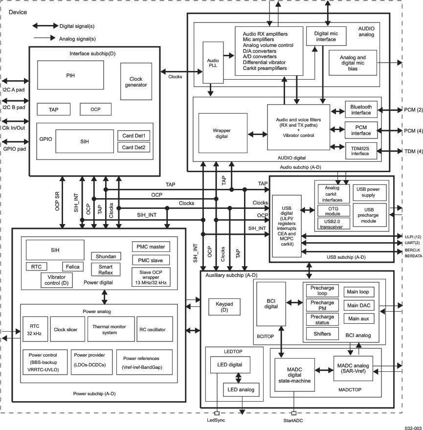 Figure 1-1 TPS65950 Functional Block Diagram