SBAS773A September 2017 – December 2017 ADS7142
PRODUCTION DATA.
- 1 Features
- 2 Applications
- 3 Description
- 4 Revision History
- 5 Pin Configuration and Functions
-
6 Specifications
- 6.1 Absolute Maximum Ratings
- 6.2 ESD Ratings
- 6.3 Recommended Operating Conditions
- 6.4 Thermal Information
- 6.5 Electrical Characteristics - All Modes
- 6.6 Electrical Characteristics - Manual Mode
- 6.7 Electrical Characteristics - Autonomous Modes
- 6.8 Electrical Characteristics - High Precision Mode
- 6.9 Timing Requirements
- 6.10 Switching Characteristics
- 6.11 Typical Characteristics for All Modes
- 6.12 Typical Characteristics for Manual Mode
- 6.13 Typical Characteristics for Autonomous Modes
- 6.14 Typical Characteristics for High Precision Mode
-
7 Detailed Description
- 7.1 Overview
- 7.2 Functional Block Diagram
- 7.3 Feature Description
- 7.4 Device Functional Modes
- 7.5 Optimizing Power Consumed by the Device
- 7.6
Register Map
- 7.6.1 RESET REGISTERS
- 7.6.2 FUNCTIONAL MODE SELECT REGISTERS
- 7.6.3 INPUT CONFIG REGISTER
- 7.6.4 ANALOG MUX and SEQUENCER REGISTERS
- 7.6.5 OSCILLATOR and TIMING CONTROL REGISTERS
- 7.6.6 DATA BUFFER CONTROL REGISTER
- 7.6.7
ACCUMULATOR CONTROL REGISTERS
- 7.6.7.1 ACC_EN Register (address = 30h), [reset = 00h]
- 7.6.7.2 ACC_CH0_LSB Register (address = 08h), [reset = 00h]
- 7.6.7.3 ACC_CH0_MSB Register (address = 09h), [reset = 00h]
- 7.6.7.4 ACC_CH1_LSB Register (address = 0Ah), [reset = 00h]
- 7.6.7.5 ACC_CH1_MSB Register (address = 0Bh), [reset = 00h]
- 7.6.7.6 ACCUMULATOR_STATUS Register (address = 02h), [reset = 00h]
- 7.6.8
DIGITAL WINDOW COMPARATOR REGISTERS
- 7.6.8.1 ALERT_DWC_EN Register (address = 37h), [reset = 00h]
- 7.6.8.2 ALERT_CHEN (address = 34h), [reset = 00h]
- 7.6.8.3 DWC_HTH_CH0_MSB Register (address = 39h), [reset = 00h]
- 7.6.8.4 DWC_HTH_CH0_LSB Register (address = 38h), [reset = 00h]
- 7.6.8.5 DWC_LTH_CH0_MSB Register (address = 3Bh), [reset = 00h]
- 7.6.8.6 DWC_LTH_CH0_LSB Register (address = 3Ah), [reset = 00h]
- 7.6.8.7 DWC_HYS_CH0 (address = 40h), [reset = 00h]
- 7.6.8.8 DWC_HTH_CH1_MSB Register (address = 3Dh), [reset = 00h]
- 7.6.8.9 DWC_HTH_CH1_LSB Register (address = 3Ch), [reset = 00h]
- 7.6.8.10 DWC_LTH_CH1_MSB Register (address = 3Fh), [reset = 00h]
- 7.6.8.11 DWC_LTH_CH1_LSB Register (address = 3Eh), [reset = 00h]
- 7.6.8.12 DWC_HYS_CH1 (address = 41h), [reset = 00h]
- 7.6.8.13 PRE_ALT_MAX_EVENT_COUNT Register (address = 36h), [reset = 00h]
- 7.6.8.14 ALERT_TRIG_CHID Register (address = 03h), [reset = 00h]
- 7.6.8.15 ALERT_LOW_FLAGS Register (address = 0C), [reset = 00h]
- 7.6.8.16 ALERT_HIGH_FLAGS Register (address = 0Eh), [reset = 00h]
- 8 Application and Implementation
- 9 Power-Supply Recommendations
- 10Layout
- 11Device and Documentation Support
- 12Mechanical, Packaging, and Orderable Information
Package Options
Mechanical Data (Package|Pins)
- RUG|10
Thermal pad, mechanical data (Package|Pins)
Orderable Information
1 Features
- Standalone, Nanopower Sensor Monitor for
Cost-sensitive Designs - Small Package Size: 1.5 mm x 2 mm
- Efficient Host Sleep and Wake-up
- Autonomous Monitoring at 900 nW
- Windowed Comparator for Event-triggered Host Wake-up
- Data Buffering during Host Sleep
- Independent Sensor Configuration and Calibration
- Dual-Channel, Pseudo-Differential, or Ground-Sense Input Configuration
- Programmable Thresholds for Calibration
- Internal Calibration improves Offset and Drift
- False Trigger Prevention
- Programmable Thresholds per Channel
- Programmable Hysteresis for Noise Immunity
- Event Counter for Transient Rejection
- Deep Data Analysis
- Data Buffer for Fault Diagnostics
- High Precision Mode for 16-bit Accuracy
- One-Shot Mode for Fast Data Capture
- I2C™ Interface
- Compatible from 1.65 V to 3.6 V
- 8 Configurable Addresses
- Up to 3.4 MHz (High Speed)
- Wide Operating Range
- Analog Supply: 1.65 V to 3.6 V
- Temperature Range: –40°C to 125°C
2 Applications
- Sensor Nodes for Internet of Things (IoT)
- Gas, Heat, PIR Motion and Smoke Detectors
- Preventive Maintenance for Elevators, Escalators, HVAC, Industrial Equipment, and so forth
- Wearable Electronics
- Zero Cross Detection for Fault Indicators
- Supervisory Functions
- Comparator with Programmable Reference
- Sensors for Deep Learning Artificial Intelligence
3 Description
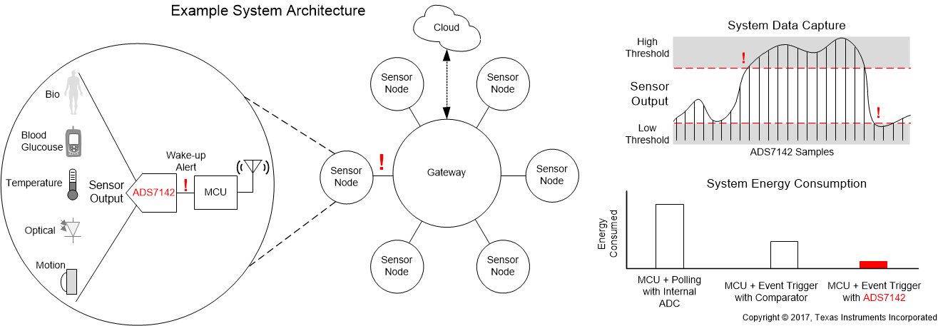
The ADS7142 autonomously monitors signals while optimizing system power, reliability, and performance. It implements event-triggered interrupts per channel using a digital windowed comparator with programmable high and low thresholds, hysteresis, and event counter. The device includes a dual-channel analog multiplexer in front of a successive approximation register analog-to-digital converter (SAR ADC) followed by an internal data buffer for converting and capturing data from sensors.
The ADS7142 is available in 10-pin QFN package and consumes only 900 nW of power. The small form-factor and low power consumption make this device suitable for space-constrained and/or battery-powered applications.
Device Information(1)
| PART NAME | PACKAGE | BODY SIZE (NOM) |
|---|---|---|
| ADS7142 | X2QFN (10) | 1.50 mm × 2.00 mm |
- For all available packages, see the orderable addendum at the end of the datasheet.
