SLUSC67B March 2016 – October 2017
PRODUCTION DATA.
- 1 Features
- 2 Applications
- 3 Description
- 4 Revision History
- 5 Pin Configuration and Functions
-
6 Specifications
- 6.1 Absolute Maximum Ratings
- 6.2 ESD Ratings
- 6.3 Recommended Operating Conditions
- 6.4 Thermal Information
- 6.5 Electrical Characteristics: Supply Current
- 6.6 Electrical Characteristics: Power Supply Control
- 6.7 Electrical Characteristics: AFE Power-On Reset
- 6.8 Electrical Characteristics: AFE Watchdog Reset and Wake Timer
- 6.9 Electrical Characteristics: Current Wake Comparator
- 6.10 Electrical Characteristics: VC1, VC2, VC3, VC4, BAT, PACK
- 6.11 Electrical Characteristics: SMBD, SMBC
- 6.12 Electrical Characteristics: PRES, BTP_INT, DISP
- 6.13 Electrical Characteristics: LEDCNTLA, LEDCNTLB, LEDCNTLC
- 6.14 Electrical Characteristics: Coulomb Counter
- 6.15 Electrical Characteristics: CC Digital Filter
- 6.16 Electrical Characteristics: ADC
- 6.17 Electrical Characteristics: ADC Digital Filter
- 6.18 Electrical Characteristics: CHG, DSG FET Drive
- 6.19 Electrical Characteristics: PCHG FET Drive
- 6.20 Electrical Characteristics: FUSE Drive
- 6.21 Electrical Characteristics: Internal Temperature Sensor
- 6.22 Electrical Characteristics: TS1, TS2, TS3, TS4
- 6.23 Electrical Characteristics: PTC, PTCEN
- 6.24 Electrical Characteristics: Internal 1.8-V LDO
- 6.25 Electrical Characteristics: High-Frequency Oscillator
- 6.26 Electrical Characteristics: Low-Frequency Oscillator
- 6.27 Electrical Characteristics: Voltage Reference 1
- 6.28 Electrical Characteristics: Voltage Reference 2
- 6.29 Electrical Characteristics: Instruction Flash
- 6.30 Electrical Characteristics: Data Flash
- 6.31 Electrical Characteristics: OCD, SCC, SCD1, SCD2 Current Protection Thresholds
- 6.32 Timing Requirements: OCD, SCC, SCD1, SCD2 Current Protection Timing
- 6.33 Timing Requirements: SMBus
- 6.34 Timing Requirements: SMBus XL
- 6.35 Typical Characteristics
-
7 Detailed Description
- 7.1 Overview
- 7.2 Functional Block Diagram
- 7.3
Feature Description
- 7.3.1 Primary (1st Level) Safety Features
- 7.3.2 Secondary (2nd Level) Safety Features
- 7.3.3 Charge Control Features
- 7.3.4 Gas Gauging
- 7.3.5 Configuration
- 7.3.6 Battery Parameter Measurements
- 7.3.7 Battery Trip Point (BTP)
- 7.3.8 Lifetime Data Logging Features
- 7.3.9 Authentication
- 7.3.10 LED Display
- 7.3.11 Voltage
- 7.3.12 Current
- 7.3.13 Temperature
- 7.3.14 Communications
- 7.4 Device Functional Modes
- 8 Applications and Implementation
- 9 Power Supply Recommendations
- 10Layout
- 11Device and Documentation Support
- 12Mechanical, Packaging, and Orderable Information
Package Options
Mechanical Data (Package|Pins)
- RSM|32
Thermal pad, mechanical data (Package|Pins)
- RSM|32
Orderable Information
1 Features
- High-Side Protection N-CH FET Drive Enables Serial Bus Communication During Fault Conditions
- Cell Balancing with Internal Bypass Optimizes Battery Health
- Diagnostic Lifetime Data Monitor and Black Box Recorder for Failure Analysis
- Full Array of Programmable Protection Features: Voltage, Current, Temperature
- JEITA Charge Algorithms Support Smart Charging
- Analog Front End with Two Independent ADCs
- Simultaneous Current and Voltage Sampling
- High-Accuracy Coulomb Counter with Input Offset Error < 1 μV (Typical)
- Supports Battery Trip Point (BTP) Function for Windows® Integration
- LED Display for State of Charge and Battery Status Indication
- 100-KHz SMBus v1.1 Communications Interface for Programming and Data Access with Alternate 400-KHz Mode
- SHA-1 Authentication Responder for Increased Battery Pack Security
- Compact 32-Pin VQFN Package (RSM)
2 Applications
- Notebooks
- Medical and Test Equipment
- Portable Instrumentation
- Cordless Vacuum Cleaners and Vacuum Robots
3 Description
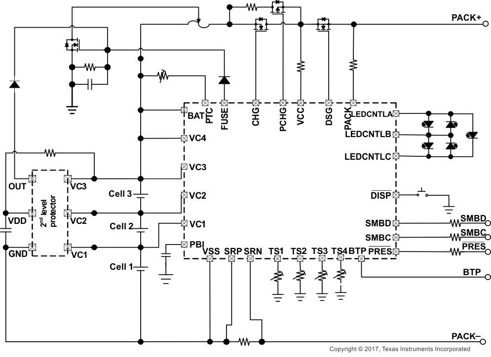
The Texas Instruments bq4050 device, incorporating Compensated End-of-Discharge Voltage (CEDV) technology, is a highly integrated, accurate, 1-series to 4-series cell gas gauge and protection solution, enabling autonomous charger control and cell balancing.
The bq4050 device provides a fully integrated pack-based solution with a flash programmable custom reduced instruction-set CPU (RISC), safety protection, and authentication for Li-Ion and Li-Polymer battery packs.
The bq4050 gas gauge communicates via an SMBus-compatible interface and combines an ultra-low power, high-speed TI bqBMP processor, high-accuracy analog measurement capabilities, integrated flash memory, an array of peripheral and communication ports, an N-CH FET drive, and a SHA-1 Authentication transform responder into a complete, high-performance battery management solution.
Device Information(1)
| PART NUMBER | PACKAGE | BODY SIZE (NOM) |
|---|---|---|
| bq4050 | VQFN (32) | 4.00 mm × 4.00 mm |
- For all available packages, see the orderable addendum at the end of this data sheet.
Simplified Schematic
