SNVS487E December 2006 – January 2015 LM27313 , LM27313-Q1
PRODUCTION DATA.
- 1 Features
- 2 Applications
- 3 Description
- 4 Revision History
- 5 Pin Configuration and Functions
- 6 Specifications
- 7 Detailed Description
-
8 Application and Implementation
- 8.1 Application Information
- 8.2
Typical Applications
- 8.2.1
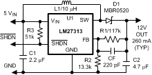
Application Circuit VIN=5.0 V, VOUT=12.0 V, Iload=250 mA
- 8.2.1.1 Design Requirements
- 8.2.1.2
Detailed Design Procedure
- 8.2.1.2.1 Selecting the External Capacitors
- 8.2.1.2.2 Selecting the Output Capacitor
- 8.2.1.2.3 Selecting the Input Capacitor
- 8.2.1.2.4 Feed-Forward Compensation
- 8.2.1.2.5 Selecting Diodes
- 8.2.1.2.6 Setting the Output Voltage
- 8.2.1.2.7 Duty Cycle
- 8.2.1.2.8 Inductance Value
- 8.2.1.2.9 Maximum Switch Current
- 8.2.1.2.10 Calculating Load Current
- 8.2.1.2.11 Design Parameters VSW and ISW
- 8.2.1.2.12 Minimum Inductance
- 8.2.1.2.13 Inductor Suppliers
- 8.2.1.2.14 Shutdown Pin Operation
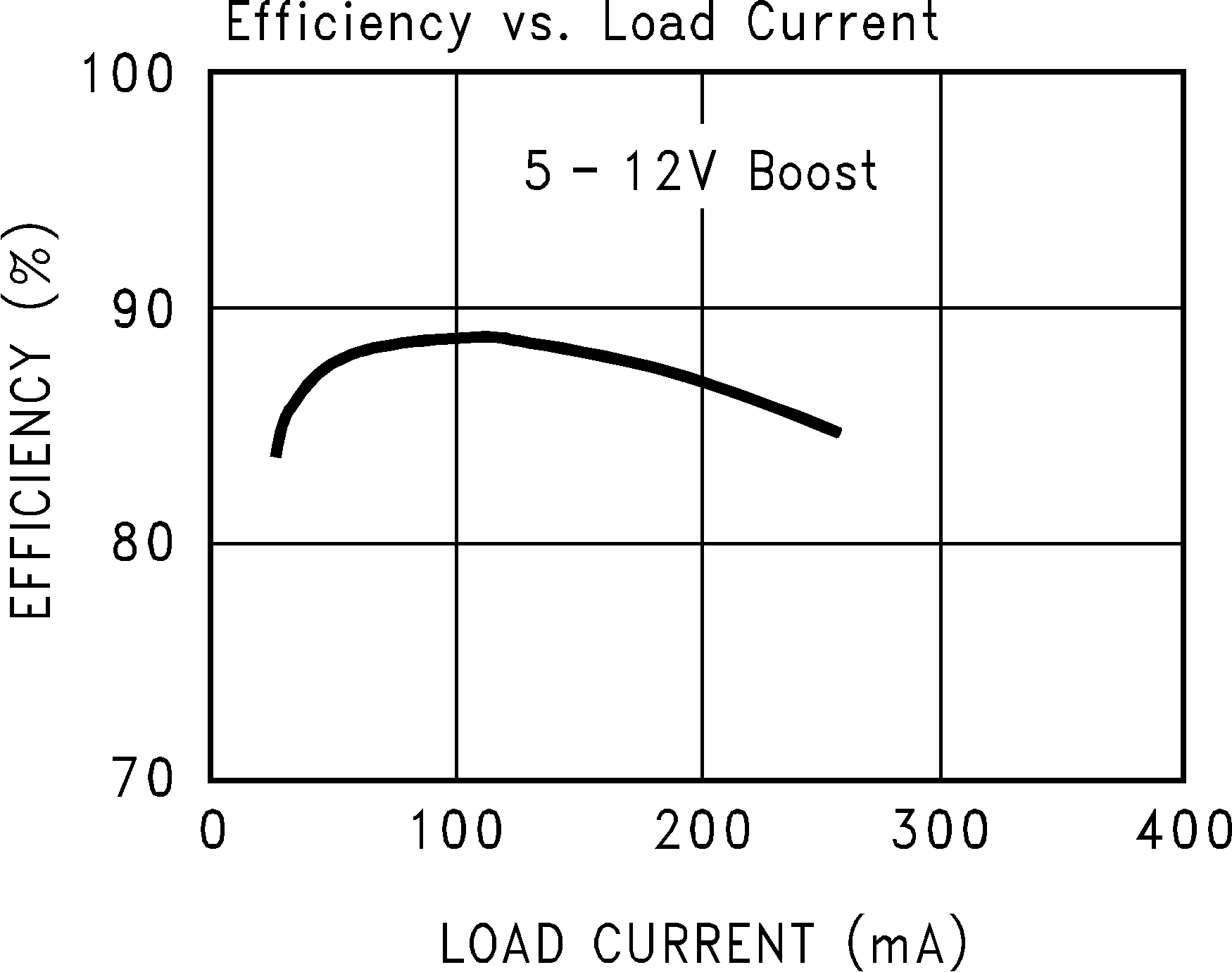
- 8.2.1.3 Application Curves
- 8.2.2 Application Circuit VIN=5.0V, VOUT=20.0V, Iload=150mA
- 8.2.1
Application Circuit VIN=5.0 V, VOUT=12.0 V, Iload=250 mA
- 9 Power Supply Recommendations
- 10Layout
- 11Device and Documentation Support
- 12Mechanical, Packaging, and Orderable Information
Package Options
Mechanical Data (Package|Pins)
- DBV|5
Thermal pad, mechanical data (Package|Pins)
Orderable Information
1 Features
- LM27313-Q1 is an Automotive-Grade Product that is AEC-Q100 Grade 1 Qualified (–40°C to +125°C Operating Junction Temperature)
- 30-V DMOS FET Switch
- 1.6-MHz Switching Frequency
- Low RDS(ON) DMOS FET
- Switch Current up to 800 mA
- Wide Input Voltage Range (2.7 V to 14 V)
- Low Shutdown Current (< 1 µA)
- 5-Lead SOT-23 Package
- Uses Tiny Capacitors and Inductors
- Cycle-by-Cycle Current Limiting
- Internally Compensated
2 Applications
- White LED Current Source
- PDAs and Palm-Top Computers
- Digital Cameras
- Portable Phones, Games, and Media Players
- GPS Devices
3 Description
The LM27313/-Q1 switching regulator is a current-mode boost converter with a fixed operating frequency of 1.6 MHz.
The use of the SOT-23 package, made possible by the minimal losses of the 800-mA switch, and the small inductors and capacitors result in extremely high power density. The 30-V internal switch makes these solutions perfect for boosting to voltages of 5 V to 28 V.
This device has a logic-level shutdown pin that can be used to reduce quiescent current and extend battery life.
Protection is provided through cycle-by-cycle current limiting and thermal shutdown. Internal compensation simplifies design and reduces component count.
Device Information(1)
| PART NUMBER | PACKAGE | BODY SIZE (NOM) |
|---|---|---|
| LM27313 | SOT-23 (5) | 2.90 mm x 1.60 mm |
| LM27313-Q1 |
- For all available packages, see the orderable addendum at the end of the data sheet.
Typical Application Circuit
Efficiency vs. Load Current