SNAS692A January 2017 – May 2017 LMK61E0M
PRODUCTION DATA.
- 1 Features
- 2 Applications
- 3 Description
- 4 Revision History
- 5 Pin Configuration and Functions
-
6 Specifications
- 6.1 Absolute Maximum Ratings
- 6.2 ESD Ratings
- 6.3 Recommended Operating Conditions
- 6.4 Thermal Information
- 6.5 Electrical Characteristics - Power Supply
- 6.6 3.3-V LVCMOS Output Characteristics
- 6.7 OE Input Characteristics
- 6.8 ADD Input Characteristics
- 6.9 Frequency Tolerance Characteristics
- 6.10 Frequency Margining Characteristics
- 6.11 Power-On/Reset Characteristics (VDD)
- 6.12 I2C-Compatible Interface Characteristics (SDA, SCL)
- 6.13 Other Characteristics
- 6.14 PLL Clock Output Jitter Characteristics
- 6.15 Additional Reliability and Qualification
- 6.16 Typical Characteristics
- 7 Parameter Measurement Information
-
8 Detailed Description
- 8.1 Overview
- 8.2 Functional Block Diagram
- 8.3
Feature Description
- 8.3.1 Device Block-Level Description
- 8.3.2 Device Configuration Control
- 8.3.3 Register File Reference Convention
- 8.3.4 Configuring the PLL
- 8.3.5 Integrated Oscillator
- 8.3.6 Reference Divider and Doubler
- 8.3.7 Phase Frequency Detector
- 8.3.8 Feedback Divider (N)
- 8.3.9 Fractional Engine
- 8.3.10 Charge Pump
- 8.3.11 Loop Filter
- 8.3.12 VCO Calibration
- 8.3.13 High-Speed Output Divider
- 8.3.14 High-Speed Clock Output
- 8.3.15 Device Status
- 8.4 Device Functional Modes
- 8.5 Programming
- 8.6
Register Maps
- 8.6.1
Register Descriptions
- 8.6.1.1 VNDRID_BY1 Register; R0
- 8.6.1.2 VNDRID_BY0 Register; R1
- 8.6.1.3 PRODID Register; R2
- 8.6.1.4 REVID Register; R3
- 8.6.1.5 SLAVEADR Register; R8
- 8.6.1.6 EEREV Register; R9
- 8.6.1.7 DEV_CTL Register; R10
- 8.6.1.8 XO_CAPCTRL_BY1 Register; R16
- 8.6.1.9 XO_CAPCTRL_BY0 Register; R17
- 8.6.1.10 CMOSCTL Register; R20
- 8.6.1.11 DIFFCTL Register; R21
- 8.6.1.12 OUTDIV_BY1 Register; R22
- 8.6.1.13 OUTDIV_BY0 Register; R23
- 8.6.1.14 RDIVCMOSCTL Register; R24
- 8.6.1.15 PLL_NDIV_BY1 Register; R25
- 8.6.1.16 PLL_NDIV_BY0 Register; R26
- 8.6.1.17 PLL_FRACNUM_BY2 Register; R27
- 8.6.1.18 PLL_FRACNUM_BY1 Register; R28
- 8.6.1.19 PLL_FRACNUM_BY0 Register; R29
- 8.6.1.20 PLL_FRACDEN_BY2 Register; R30
- 8.6.1.21 PLL_FRACDEN_BY1 Register; R31
- 8.6.1.22 PLL_FRACDEN_BY0 Register; R32
- 8.6.1.23 PLL_MASHCTRL Register; R33
- 8.6.1.24 PLL_CTRL0 Register; R34
- 8.6.1.25 PLL_CTRL1 Register; R35
- 8.6.1.26 PLL_LF_R2 Register; R36
- 8.6.1.27 PLL_LF_C1 Register; R37
- 8.6.1.28 PLL_LF_R3 Register; R38
- 8.6.1.29 PLL_LF_C3 Register; R39
- 8.6.1.30 PLL_CALCTRL Register; R42
- 8.6.1.31 NVMSCRC Register; R47
- 8.6.1.32 NVMCNT Register; R48
- 8.6.1.33 NVMCTL Register; R49
- 8.6.1.34 MEMADR Register; R51
- 8.6.1.35 NVMDAT Register; R52
- 8.6.1.36 RAMDAT Register; R53
- 8.6.1.37 NVMUNLK Register; R56
- 8.6.1.38 INT_LIVE Register; R66
- 8.6.1.39 SWRST Register; R72
- 8.6.1
Register Descriptions
- 9 Application and Implementation
- 10Power Supply Recommendations
- 11Layout
- 12Device and Documentation Support
- 13Mechanical, Packaging, and Orderable Information
Package Options
Mechanical Data (Package|Pins)
- SIA|8
Thermal pad, mechanical data (Package|Pins)
Orderable Information
1 Features
-
Ultra-Low Noise, High Performance
- Jitter: 500-fs RMS Typical fOUT > 50 MHz on LMK61E0M
- LMK61E0M Supports 3.3-V LVCMOS Output up to 200 MHz
- Total Frequency Tolerance of ±25 ppm
- System Level Features
- Glitch-Less Frequency Margining: Up to ±1000 ppm From Nominal
- Internal EEPROM: User Configurable Start-Up Settings
- Other Features
- Device Control: Fast Mode I2C up to 1000 kHz
- 3.3-V Operating Voltage
- Industrial Temperature Range (–40ºC to +85ºC)
- 7-mm × 5-mm 8-Pin Package
- Default Frequency: 70.656 MHz
2 Applications
- High-Performance Replacement for Crystal, SAW, or Silicon-Based Oscillators
- Switches, Routers, Network Line Cards, Base Band Units (BBU), Servers, Storage/SAN
- Test and Measurement
- Medical Imaging
- FPGA, Processor Attach
- xDSL, Broadcast Video
3 Description
The LMK61E0 family of ultra-low jitter PLLatinumTM programmable oscillators use fractional-N frequency synthesizers with integrated VCOs to generate commonly used reference clocks. The LMK61E0M supports 3.3-V LVCMOS outputs. The device features self start-up from on-chip EEPROM to generate a factory programmed default output frequency, or the device registers and EEPROM settings are fully programmable in-system through I2C serial interface. The device provides fine and coarse frequency margining control through I2C serial interface, making it a digitally-controlled oscillator (DCXO).
The PLL feedback divider can be updated to adjust the output frequency without spikes or glitches in steps of <1ppb using a PFD of 12.5 MHz (R divider=4, doubler disabled) for compatibility with xDSL requirements, or in steps of <5.2 ppb using a PFD of 100 MHz (R divider=1, doubler enabled) for compatibility with broadcast video requirements. The frequency margining features also facilitate system design verification tests (DVT), such as standards compliance and system timing margin testing.
Device Information(1)
| PART NUMBER | PACKAGE | BODY SIZE (NOM) |
|---|---|---|
| LMK61E0M | QFM (8) | 7.00 mm × 5.00 mm |
- For all available packages, see the orderable addendum at the end of the data sheet.
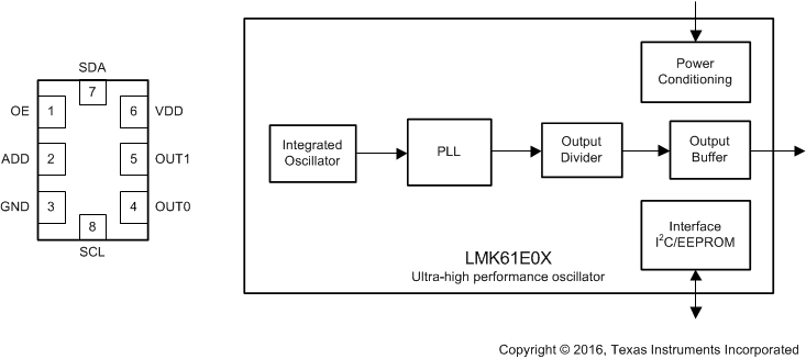
Pinout and Simplified Block Diagram
