SNOS976M November 2001 – September 2016 LMV981-N , LMV982-N
PRODUCTION DATA.
- 1 Features
- 2 Applications
- 3 Description
- 4 Revision History
- 5 Description (continued)
- 6 Pin Configuration and Functions
-
7 Specifications
- 7.1 Absolute Maximum Ratings
- 7.2 ESD Ratings
- 7.3 Recommended Operating Conditions
- 7.4 Thermal Information
- 7.5 Electrical Characteristics - DC, 1.8 V
- 7.6 Electrical Characteristics - AC, 1.8 V
- 7.7 Electrical Characteristics - DC, 2.7 V
- 7.8 Electrical Characteristics - AC, 2.7 V
- 7.9 Electrical Characteristics - DC, 5 V
- 7.10 Electrical Characteristics - AC, 5 V
- 7.11 Typical Characteristics
- 8 Detailed Description
- 9 Application and Implementation
- 10Power Supply Recommendations
- 11Layout
- 12Device and Documentation Support
- 13Mechanical, Packaging, and Orderable Information
Package Options
Mechanical Data (Package|Pins)
Thermal pad, mechanical data (Package|Pins)
- DCK|6
Orderable Information
1 Features
- Ensured 1.8-V, 2.7-V, and 5-V Specifications
- Output Swing:
- 600-Ω Load: 80-mV from Rail
- 2-kΩ Load: 30-mV from Rail
- VCM 200 mV Beyond Rails
- Supply Current (Per Channel): 100 µA
- Gain Bandwidth Product: 1.4 MHz
- Maximum VOS: 4 mV
- Gain with 600-Ω Load: 101 dB
- Ultra-Small Package: DSBGA 1.0 mm × 1.5 mm
- Turnon Time from Shutdown: 19 µs
- Independent Shutdown on Dual
- Temperature Range: −40°C to 125°C
2 Applications
- Industrial and Automotive
- Consumer Communication
- Fitness Trackers
- Wearables
- Mobile Phones
- Portable Audio
- Portable and Battery-Powered Electronic Equipment
- Supply Current Monitoring
- Battery Monitoring
3 Description
LMV98x-N are low-voltage, low-power operational amplifiers. LMV98x-N operate from 1.8-V to 5-V supply voltages and have rail-to-rail input and output. LMV98x-N input common mode voltage extends 200mV beyond the supplies which enables user enhanced functionality beyond the supply voltage range. The output can swing rail-to-rail unloaded and within 105 mV from the rail with 600-Ω load at 1.8-V supply. LMV98x-N are optimized to work at 1.8 V, which makes them ideal for portable two-cell battery powered systems and single cell Li-Ion systems.
LMV98x-N offer a shutdown pin that can be used to disable the device and reduce the supply current. The device is in shutdown when the SHDN pin is low. The output is high impedance in shutdown.
LMV98x-N exhibit excellent speed-power ratio, achieving 1.4-MHz gain bandwidth product at 1.8-V supply voltage with low supply current. LMV98x-N are capable of driving a 600-Ω load and up to 1000-pF capacitive load with minimal ringing. LMV98x-N have a high DC gain of 101 dB, making them suitable for low frequency applications.
Device Information(1)
| PART NUMBER | PACKAGE | BODY SIZE (NOM) |
|---|---|---|
| LMV981-N | DSBGA (6) | 1.50 mm × 1.30 mm |
| SC70 (6) | 2.00 mm × 1.25 mm | |
| SOT-23 (6) | 2.90 mm × 1.60 mm | |
| LMV982-N | VSSOP (10) | 3.00 mm × 3.00 mm |
- For all available packages, see the orderable addendum at the end of the data sheet.
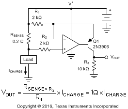
Typical Application

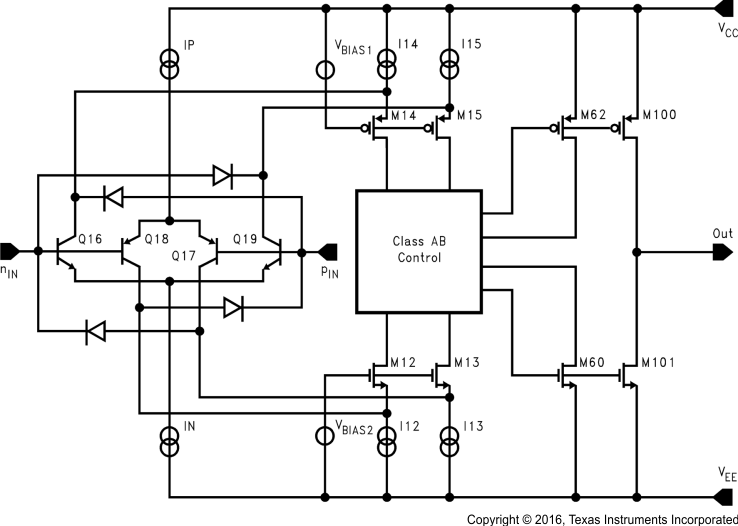
Simplified Schematic
