SNOS510Q November 1999 – October 2016 LP2985LV-N
PRODUCTION DATA.
- 1 Features
- 2 Applications
- 3 Description
- 4 Revision History
- 5 Pin Configuration and Functions
- 6 Specifications
- 7 Detailed Description
-
8 Application and Implementation
- 8.1 Application Information
- 8.2 Typical Application
- 9 Power Supply Recommendations
- 10Layout
- 11Device and Documentation Support
- 12Mechanical, Packaging, and Orderable Information
Package Options
Mechanical Data (Package|Pins)
- DBV|5
Thermal pad, mechanical data (Package|Pins)
Orderable Information
1 Features
- Wide Supply Voltage Range: 2.2 V to 16 V
- Ensured 150-mA Output Current
- Requires Minimum External Components
- Stable With Low-ESR Output Capacitor
- < 1-µA Quiescent Current When Shut Down
- Low Ground Pin Current at all Loads
- Output Voltage Accuracy 1% (A Grade)
- High Peak Current Capability
- Low ZOUT: 0.3-Ω Typical (10 Hz to 1 MHz)
- Overtemperature/Overcurrent Protection
- −40°C to +125°C Junction Temperature Range
2 Applications
- Cellular Phone
- Palmtop/Laptop Computer
- Personal Digital Assistant (PDA)
- Camcorder, Personal Stereo, Camera
3 Description
The LP2985LV-N is a 150-mA, fixed-output voltage regulator designed to provide high performance and low noise in applications requiring output voltages ≤ 2 V.
Using an optimized vertically integrated PNP (VIP) process, the LP2985LV-N delivers unequaled performance in all specifications critical to battery-powered designs:
- Ground Pin Current: Typically 825 µA at 150-mA load, and 75 µA at 1-mA load.
- Enhanced Stability: The LP2985LV-N is stable with output capacitor equivalent series resistance (ESR) as low as 5 mΩ, which allows the use of ceramic capacitors on the output.
- Sleep Mode: Less than 1-µA quiescent current when ON/OFF pin is pulled low.
- Precision Output: 1% tolerance output voltages available (A grade).
- Low Noise: By adding a 10-nF bypass capacitor, output noise can be reduced to 30 µV (typical).
Device Information(1)
| PART NUMBER | PACKAGE | BODY SIZE (NOM) |
|---|---|---|
| LP2985LV-N | SOT-23 (5) | 2.90 mm × 1.60 mm |
| DSBGA (5) | 1.164 mm × 0.987 mm |
- For all available packages, see the orderable addendum at the end of the data sheet.
Space
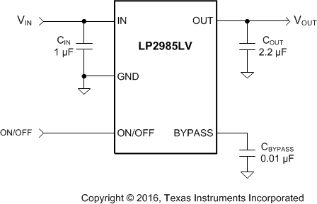
Typical Application
